
Key Statistics
Key Takeaways
- Standard glass core substrates remain the commercial entry point because they provide the dimensional stability and low-loss electrical behavior needed for advanced packages without requiring the most demanding thermal or dielectric formulations. High-thermal-conductivity and low-dielectric-loss variants are gaining importance as AI accelerators move toward larger package footprints and higher interconnect densities.
- High-performance computing and AI accelerators form the strongest demand cluster. Glass addresses package warpage, routing density, high-speed signaling and power-delivery constraints that become more severe as logic, HBM and chiplets are integrated in increasingly large 2.5D and 3D architectures.
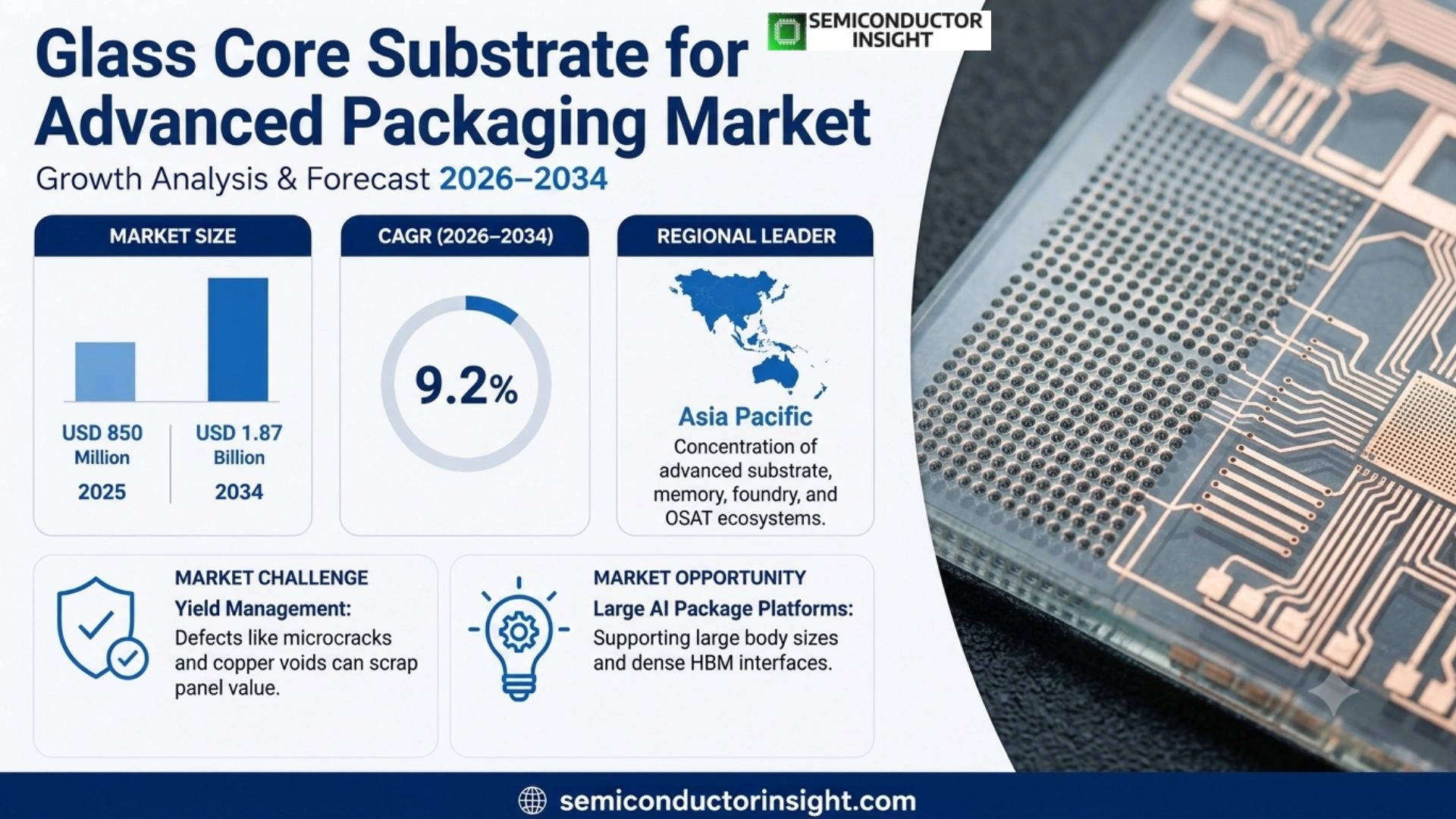
- Asia Pacific is the largest regional market because the commercial ecosystem for advanced substrates, memory, foundry production, OSAT services and electronics manufacturing is concentrated in South Korea, Taiwan, Japan and China. The region therefore captures both substrate development and the downstream package-assembly pull.
- North America has the strongest near-term localization momentum, supported by U.S. advanced-packaging investment and the Absolics glass-substrate facility in Georgia. Domestic supply is strategically important because the U.S. Department of Commerce explicitly identified advanced-packaging substrate production as concentrated in Asia.
- Manufacturing yield and process maturity are the central restraints. Glass brings superior dimensional properties, but brittle-material handling, through-glass-via formation, fine-line metallization, panel uniformity and defect control can raise cost until high-volume process windows stabilize.
- Competitive advantage is shifting from material specification alone to integrated process capability. Suppliers that combine glass formulation, via formation, metallization, large-panel handling and customer qualification can capture more value than firms supplying an isolated material step.
Glass Core Substrate for Advanced Packaging Market Overview
Glass Core Substrate for Advanced Packaging Market was valued at USD 850 million in 2025 and is projected to reach USD 1.87 billion by 2034, representing a 9.2% CAGR during 2026–2034. Asia Pacific is the largest market because advanced substrate, memory, foundry and outsourced semiconductor assembly ecosystems are concentrated there, while North America is developing the strongest new domestic-capacity momentum.
A glass core substrate is a structural and electrical foundation used in advanced semiconductor packaging to route power and high-speed signals between silicon devices and the package or board. Replacing an organic core with glass can improve dimensional stability, reduce warpage, support finer interconnect geometries and provide favorable dielectric characteristics. These properties become commercially important when package sizes increase and when logic dies, high-bandwidth memory and chiplets must be connected with very short, dense electrical paths.
The market is therefore not simply a replacement-material opportunity. It sits at the intersection of advanced packaging, panel processing, interconnect scaling and heterogeneous integration. Glass enables package architects to consider larger body sizes and tighter routing rules while reducing the mechanical distortion that complicates lithography and assembly on organic cores. Intel has publicly stated that glass substrates can enable an order-of-magnitude improvement in design rules and substantially higher interconnect density, illustrating why the material is being evaluated for future AI and data-center packages rather than commodity semiconductor packages.
Commercial adoption depends on whether substrate suppliers can convert laboratory advantages into repeatable high-volume manufacturing. The relevant process stack includes glass composition and thickness control, laser or other through-glass-via formation, via metallization, redistribution-layer formation, surface preparation, inspection, singulation and assembly compatibility. Yield losses at any stage can erase the cost advantage of panel-level processing, so equipment capability and process integration matter as much as the nominal electrical properties of the glass itself.
Demand is changing now because advanced processors are reaching packaging limits at the same time that AI systems are pushing package power, memory bandwidth and interconnect density upward. Large accelerators increasingly rely on chiplet-based architectures and nearby HBM stacks. This creates a strong commercial incentive for substrate technologies that can support larger dimensions with lower warpage and tighter routing, while governments and major electronics suppliers are simultaneously investing in domestic advanced-packaging capacity and more diversified supply chains.
Segment Analysis: By Type
By type, the market is segmented into Standard Glass Core Substrate, High-Thermal Conductivity Glass Core Substrate, and Low-Dielectric Loss Glass Core Substrate. Standard products account for the broadest commercial qualification activity because they address the core dimensional-stability problem. Higher-performance formulations grow faster where package power, thermal gradients and very high signaling rates justify additional material and process cost.
| Type | Function and technical role | Market position |
|---|---|---|
| Standard Glass Core Substrate | Provides a dimensionally stable core for advanced package build-up layers, fine redistribution structures and through-glass electrical connections. The principal customer requirement is lower warpage and better registration across large package or panel formats than conventional organic cores can deliver as packages become wider and denser. | Largest commercial segment in 2025. It is the logical first qualification route because customers can validate glass handling and metallization without simultaneously depending on specialized thermal or ultra-low-loss formulations. Volume expansion is tied to AI-server, HPC and advanced-package pilot programs moving from engineering samples toward production. |
| High-Thermal Conductivity Glass Core Substrate | Targets packages where heat density and temperature gradients increase mechanical stress and reliability risk. The substrate itself is not a heat sink, but tailored glass and package-stack design can improve thermal stability and maintain registration during high-temperature processing and repeated operating cycles. | A high-value growth segment for AI accelerators, server processors and automotive compute modules. Adoption is strongest where thermal-mechanical reliability is worth a premium and where customers are already using advanced cooling, high-current power delivery and multiple high-power dies in one package. |
| Low-Dielectric Loss Glass Core Substrate | Uses glass formulations and routing structures optimized for high-frequency electrical performance. Lower dielectric loss reduces signal attenuation and supports high-speed links between compute dies, memory and package interfaces, making the segment especially relevant as package-level data rates rise. | Fastest-growing performance-oriented segment. The commercial trigger is not low loss in isolation; it is the ability to maintain high-speed signal integrity across longer package routes while also enabling dense wiring. AI, HPC and communications packages provide the strongest willingness to pay. |
Packaging technology interaction
Glass core adoption is closely linked to the packaging architecture around it. In fan-out wafer-level and panel-level approaches, glass can provide a stable carrier or core that supports fine redistribution layers across larger formats. In system-in-package configurations, it helps combine multiple functional dies and passive structures. In 2.5D and 3D integration, the value proposition strengthens because routing density, package size and warpage all become more difficult as the number of chiplets and memory stacks increases.
Segment Analysis: By Application
By application, the report scope covers High-Performance Computing, Artificial Intelligence Accelerators and 5G Infrastructure. AI accelerators are the most powerful incremental demand engine because their package sizes, HBM interfaces and power density expose the mechanical and electrical limits of organic substrates most quickly. HPC remains the broadest adjacent demand pool, while 5G infrastructure benefits from low-loss, high-frequency routing.
| Application | Demand characteristics |
|---|---|
| High-Performance Computing (HPC) | HPC processors and accelerators require large packages, high memory bandwidth and dense die-to-die connectivity. Buyers evaluate glass where organic-core warpage and routing limits constrain package scaling. The commercial decision is qualification-driven: a substrate must demonstrate stable dimensions, low defectivity and reliable metallization over long thermal cycling before it can enter mission-critical server platforms. |
| Artificial Intelligence (AI) Accelerators | Strongest incremental demand driver. AI packages combine high-current logic with multiple HBM stacks and extremely wide internal interfaces. Intel’s public glass-substrate work and Samsung Electro-Mechanics’ focus on AI/server package substrates demonstrate that suppliers are targeting exactly this high-value use case. The buyer pays for packaging headroom that enables larger, denser and more power-efficient systems. |
| 5G Infrastructure | 5G radios, baseband equipment and network acceleration require low-loss high-frequency signal paths and high reliability. Glass-core architectures can support fine routing and favorable dielectric behavior, but adoption competes with established organic and ceramic solutions. Commercial penetration is therefore expected first in high-performance modules where electrical performance justifies process change rather than across all telecom hardware. |
End-user and packaging-technology demand
The report also segments demand by end user into data centers, automotive electronics and consumer electronics, and by packaging technology into FOWLP, SiP, and 2.5D/3D integration. Data centers provide the clearest near-term value proposition because AI infrastructure supports high package ASPs and rapid design turnover. Automotive adoption is slower because qualification cycles are longer, while consumer electronics require much tighter cost and yield thresholds before glass can displace mature organic substrates.
Regional Analysis
Asia Pacific is the largest glass core substrate market, while North America has the strongest localization-driven growth opportunity. Asia Pacific combines substrate production, memory, foundry, OSAT and electronics manufacturing in a single regional ecosystem. North America is building advanced-packaging capability around AI and HPC, including publicly supported domestic glass-substrate capacity. Europe contributes process-equipment and research depth, while South America and the Middle East & Africa are mainly downstream demand markets.
How does regional demand differ across the glass core substrate market?
Regional demand is shaped less by end-device consumption than by where advanced packages are designed, fabricated, assembled and qualified. Asia Pacific captures the largest immediate substrate pull because customer engineering teams and production lines are nearby. North America is strategically important because AI processor design and CHIPS-backed packaging investment can create qualified local supply. Europe contributes enabling process technology and automotive demand, while emerging regions participate primarily through data-center and electronics investment rather than direct substrate manufacturing.
| Region | Position | Growth outlook | Demand profile | What decides supplier selection |
|---|---|---|---|---|
| Asia Pacific | Largest | High | Advanced-packaging manufacturing led | Yield at panel scale, proximity to memory/foundry/OSAT customers, fine-line capability and customer qualification |
| North America | Second / localization focus | Fastest structural expansion | AI/HPC design and domestic supply-chain led | CHIPS-supported capacity, security of supply, performance at large package sizes and co-development with leading compute customers |
| Europe | Technology-enabling market | Moderate to high | R&D, equipment and automotive led | Process precision, sustainability, automotive reliability and access to European advanced-packaging research ecosystems |
| South America | Early-stage demand | Moderate from small base | Data-center and electronics demand | Imported advanced packages, local electronics investment, cost and availability rather than local glass-core fabrication |
| Middle East & Africa | Emerging downstream market | High from small base | AI data-center and digital-infrastructure led | Access to leading processors, reliable international supply and long-term infrastructure deployment schedules |
Key Glass Core Substrate Manufacturers and Competitive Landscape
Competition is organized around the ability to move glass from a promising material into a qualified package platform. The strongest positions belong to companies that can combine substrate process development, materials control, metallization, advanced packaging and close customer engineering. Scale alone is not sufficient because early programs require extensive co-development; equally, a strong materials position without downstream package integration can leave the supplier dependent on partners for customer qualification.
The competitive field spans several roles. Package-substrate manufacturers compete on large-area process control and routing density. Materials suppliers influence glass composition, dielectric behavior and surface compatibility. OSAT and packaging companies can accelerate adoption by integrating glass into qualified package flows, while semiconductor and memory companies shape specifications through the requirements of AI, HPC and HBM systems. This creates more partnership activity than a mature commodity substrate market, because no single supplier necessarily controls the complete process stack.
Asia Pacific currently has the deepest production ecosystem, but North American localization is becoming strategically valuable. The U.S. Commerce award to Absolics shows that domestic glass-substrate capacity is being treated as supply-chain infrastructure rather than simply another materials investment. At the same time, Samsung Electro-Mechanics’ pilot and planned mass-production roadmap, together with its Sumitomo Chemical cooperation, shows how Asian suppliers are linking materials capability with package-substrate scale.
Tier structure
| Tier | Companies | Basis of competition |
|---|---|---|
| Advanced package/substrate integrators | Samsung Electronics / Samsung ecosystem, Shinko Electric Industries, Kyocera, Amkor Technology | Customer qualification, package integration, fine-line routing, large-area process control and access to AI/HPC packaging programs |
| Materials and substrate specialists | LG Chem, Isola Group, Epcos (Murata Manufacturing), Nanocores, SunSynk Materials | Material formulation, dielectric and thermal properties, surface compatibility, manufacturing consistency and ability to support substrate-process development |
| System and memory ecosystem participants | SK Hynix and other profiled electronics companies | Demand creation through HBM, advanced compute and heterogeneous-integration roadmaps; qualification influence through package reliability and electrical-performance requirements |
Key Industry Players
- Amkor Technology
- Universal Electronics Inc.
- TOSTAR Corporation
- Naftco, Inc.
- Epcos (Murata Manufacturing)
- Isola Group
- Kyocera Corporation
- Nanocores S.A.
- Shinko Electric Industries Co., Ltd.
- SunSynk Materials Co., Ltd.
- Kingsway International Corp.
- LG Chem
- Samsung Electronics Co., Ltd.
- SK Hynix
Glass Core Substrate Production Capacity Analysis
Glass-core capacity is still being built around pilot, qualification and early commercial lines rather than the mature global footprint seen in organic package substrates. Asia Pacific has the deepest potential scale because substrate and semiconductor-package manufacturing already exists there, while the United States is adding strategically supported capacity. The real capacity constraint is qualified yield: nominal panel throughput does not become sellable capacity until via formation, metallization, registration and reliability meet customer specifications.
Capacity economics are highly sensitive to panel size and defect density. Larger glass panels can distribute fixed process costs across more package area, but they also magnify the cost of breakage, dimensional nonuniformity and metallization defects. Equipment therefore needs precise handling, alignment and inspection across transparent and brittle substrates. Suppliers that achieve stable large-panel yields can convert glass’s dimensional advantage into a manufacturing advantage; suppliers that cannot will face higher scrap and slower customer qualification regardless of installed equipment count.
The supply side is also more vertically interconnected than conventional substrate procurement. Glass composition affects drilling or laser-via behavior; via quality affects metallization; metallization affects redistribution layers; and the complete substrate influences package assembly and thermal reliability. This means capacity expansion often requires coordinated qualification across materials, equipment and packaging partners. Samsung Electro-Mechanics’ glass-core material cooperation with Sumitomo Chemical and the U.S.-supported Absolics facility both illustrate this ecosystem approach.
Glass Core Substrate Market Dynamics: Drivers, Restraints and Opportunities
The market expands because AI and HPC packages are becoming larger, denser and more electrically demanding at the same time that organic-core warpage and routing constraints become harder to manage. Glass offers a route to finer interconnects and better dimensional stability, but adoption is restrained by manufacturing maturity, brittle-material handling and customer qualification cost. The largest opportunity is to make glass a scalable platform for 2.5D, 3D and panel-level packaging rather than a niche premium substrate.
MARKET DRIVERS
Drivers Impact Analysis*
| Market Factor | Directional Impact on CAGR Forecast* | Commercial Mechanism |
|---|---|---|
| AI accelerators and HBM-rich packages | +2.1 to +2.8 percentage points | Larger packages and wider die-to-memory interfaces increase routing density and warpage pressure, making glass more valuable as organic-core limits become costly. |
| Advanced packaging and chiplet scaling | +1.5 to +2.1 percentage points | 2.5D/3D architectures require dimensional stability, fine-line routing and dense vertical connectivity across multiple dies and package regions. |
| Domestic advanced-packaging investment | +0.8 to +1.3 percentage points | Public and private investment expands qualification capacity and creates regional supply options, reducing customer concern over concentrated substrate sourcing. |
AI and HPC packaging pushes organic substrates toward mechanical limits
AI accelerators combine large logic dies, multiple HBM stacks, wide interfaces and very high package power. As package area grows, organic materials can warp during processing and operation, making fine-line alignment and assembly more difficult. Glass has a lower coefficient of thermal expansion and better dimensional stability, which gives package designers more room to increase body size and routing density. The commercial effect is strongest at the high end, where packaging cost is a smaller share of total accelerator value.
Interconnect density becomes a package-level scaling problem
Transistor scaling no longer guarantees system performance if dies cannot communicate efficiently. Glass creates a stable surface for tighter design rules and dense routing; Intel has said its glass technology can support an order-of-magnitude improvement in design rules and approximately 10x higher interconnect density. This changes substrate selection from a mechanical packaging decision into a system-performance decision, widening the addressable opportunity across chiplets, HBM and optical or high-speed electrical interfaces.
Panel-level processing can improve long-term economics
One of glass’s most important commercial advantages is compatibility with large-panel processing. If through-glass vias, metallization and redistribution layers can be manufactured with stable yield on panels larger than conventional wafers, suppliers can spread process cost across more package area. The opportunity is therefore not merely a premium material ASP; it is a potential manufacturing architecture that can lower cost per package as volumes rise and process control improves.
Supply-chain localization creates strategic purchasing value
Advanced package substrates are geographically concentrated, and the U.S. Department of Commerce explicitly cited that concentration when supporting Absolics. For AI and defense-related customers, a qualified domestic or diversified supply option can carry value beyond unit price. Suppliers that combine local engineering support, traceability and secured capacity can therefore win programs even before glass reaches the cost maturity of established organic substrates.
MARKET RESTRAINTS
Restraints Impact Analysis*
| Market Factor | Directional Impact on CAGR Forecast* | Commercial Mechanism |
|---|---|---|
| Low early-stage manufacturing yield | −1.4 to −2.0 percentage points | Breakage, via defects, metallization nonuniformity and panel registration losses increase effective cost until production processes mature. |
| Qualification and switching cost | −0.8 to −1.3 percentage points | Customers must validate electrical performance, thermo-mechanical reliability, assembly compatibility and long-term supply before replacing proven organic substrates. |
| Brittle-material handling complexity | −0.5 to −0.9 percentage points | Glass requires specialized handling, edge protection, transport and inspection, adding capital and operating complexity to substrate lines. |
Yield, not installed equipment, determines economic capacity
Glass can be processed at large area, but large area also makes every defect more expensive. Microcracks, edge damage, via-wall defects, copper voids or registration errors can scrap a substantial amount of processed panel value. Early commercial lines must therefore invest heavily in metrology, automated handling and process feedback. Until defect density stabilizes, customers may see glass as technically attractive but economically uncertain, slowing the shift from pilot qualification to high-volume purchase orders.
Existing organic-substrate ecosystems are deeply qualified
Organic package substrates have decades of supplier history, established design rules, mature build-up films, known reliability behavior and global production capacity. Replacing them requires more than showing better warpage or dielectric properties. Semiconductor customers must requalify substrate materials, assembly conditions and reliability data, while equipment makers need compatible handling and inspection. This switching cost protects incumbent technologies in mainstream packages and concentrates early glass adoption in applications where performance limitations are already expensive.
Glass processing requires specialized capability
Through-glass vias, precision cutting, surface preparation and fine metallization require tools and recipes that differ from mature organic-core manufacturing. Transparent material also changes optical inspection behavior, while brittleness creates handling risk during transfer and panel transport. The added equipment and engineering burden can slow smaller suppliers and create dependence on a limited group of process specialists, particularly during the first commercial production cycles.
MARKET OPPORTUNITIES
Large AI package platforms
The largest near-term opportunity is not broad semiconductor penetration but high-value AI packages where substrate performance directly affects system scaling. Suppliers that can support large body sizes, dense HBM interfaces and high-current power delivery can enter programs with very high package value. Once qualified, those programs create recurring demand and provide manufacturing learning that can later lower cost for adjacent HPC and networking applications.
2.5D and 3D heterogeneous integration
Glass is well positioned where multiple logic, memory and I/O chiplets must be integrated in one package. Dimensional stability supports fine routing across large areas, while through-glass vias can provide vertical connectivity. The commercial opening extends to substrate makers, laser-processing equipment suppliers, metallization specialists and OSATs because customers need a complete qualified process rather than a raw sheet of glass.
Panel-level packaging scale-up
If glass-core processing can move successfully to large panels, suppliers can challenge the cost structure of wafer-sized interposer approaches for some applications. The opportunity is particularly attractive for package architectures that require large routing areas but do not need a full silicon interposer. Equipment vendors that improve panel handling, alignment, inspection and via throughput can capture value even before substrate volumes reach full maturity.
Regional supply diversification
Governments and customers increasingly value semiconductor supply-chain resilience. The Absolics investment shows that glass-core capacity can qualify for strategic industrial support because it addresses an advanced-packaging bottleneck. Similar localization opportunities can emerge in Europe and other regions as countries seek deeper packaging capability, creating openings for joint ventures, technology licensing, equipment sales and local engineering services.
Glass Core Substrate Supply Chain Analysis
The glass-core supply chain has four tightly connected stages: specialty glass and chemicals, precision panel and via processing, metallization and substrate build-up, and final advanced-package assembly and qualification. Value capture rises as the product moves downstream because each stage adds customer-specific process knowledge. The principal bottleneck is the interface between stages: a glass panel that meets material specifications can still fail commercially if via quality, metallization adhesion or package reliability is not repeatable.
Stage 1 – Specialty glass and process materials
Upstream suppliers capture value through composition control, sheet flatness, thickness uniformity, surface quality and compatibility with downstream metallization. Small changes in glass properties can affect laser drilling, via-wall quality or thermal behavior, so substrate manufacturers need consistent lots and detailed process support. This makes materials qualification sticky: once a glass formulation is tuned into a production flow, changing suppliers can require expensive reoptimization.
Stage 2 – Panel formation and through-glass vias
This stage contains some of the most visible technical bottlenecks. High-throughput via formation must avoid cracks and maintain geometry across a large panel, while handling systems must prevent edge damage. Equipment productivity directly affects substrate economics because thousands of vias may be required per package. Suppliers that can increase via throughput while maintaining defect control can improve both line capacity and customer confidence in large-scale glass processing.
Stage 3 – Metallization and fine-line redistribution
Metallization converts structural glass into an electrical platform. Adhesion, via fill, copper uniformity, dielectric build-up and fine-pattern registration determine whether the substrate can support high-speed interconnects. Because glass is dimensionally stable, it can enable tighter routing, but only if lithography and plating processes can exploit that stability. This stage therefore captures substantial process IP and is central to differentiating one supplier’s yield and electrical performance from another’s.
Stage 4 – Package assembly and qualification
The final stage creates the deepest commercial lock-in. AI and HPC customers qualify substrates inside complete packages, including die attach, HBM integration, thermal cycling, power delivery and board-level reliability. Qualification can take many months, but once the substrate is embedded in a high-volume package, switching suppliers becomes difficult. For this reason, early co-development with semiconductor and OSAT customers is a more powerful market-entry strategy than selling glass as a standardized catalog material.
Recent Developments in the Glass Core Substrate Market
Samsung Electro-Mechanics signed an MOU with Sumitomo Chemical Group to establish a joint venture for manufacturing glass core used in package substrates. The move is commercially important because it links a major package-substrate producer with a specialized materials group, strengthening control over an upstream input that affects dimensional quality, processability and long-term supply as AI-related qualification programs advance.
Samsung Electro-Mechanics displayed glass core substrates alongside high-end AI, server and automotive package-substrate technologies at KPCA Show 2025. Positioning glass within the same roadmap as large-area, high-layer FCBGA and next-generation package structures shows that commercialization is being driven by established substrate suppliers serving demanding compute customers rather than by isolated materials experimentation.
At CES 2025, Samsung Electro-Mechanics said it had established a glass package-substrate pilot line at its Sejong site and planned customer sample promotion during 2025, with mass production targeted for 2027. This gives the market a concrete timeline from pilot processing to commercial scale and increases pressure on equipment, materials and competing substrate suppliers to demonstrate comparable production readiness.
The U.S. Department of Commerce finalized up to USD 75 million in direct funding for Absolics to support a 120,000-square-foot facility in Covington, Georgia. Commerce said the project would expand domestic supply of glass substrates for advanced packaging and support AI and high-performance-compute chips, creating a strategically backed North American production base in a market otherwise concentrated in Asia.
Intel announced one of the industry’s first glass substrates for next-generation advanced packaging and stated that the technology can enable roughly 10x higher interconnect density while supporting larger package form factors. The development established a clear high-end compute use case for glass and linked the substrate directly to future data-center, AI and trillion-transistor package roadmaps.
REPORT SCOPE & SEGMENTATION
| Study Period | 2021–2034 |
| Base Year | 2025 |
| Estimated Year | 2026 |
| Forecast Period | 2026–2034 |
| Historical Period | 2021–2025 |
| Market Size 2025 | USD 850 Million |
| Market Size 2034 | USD 1.87 Billion |
| Growth Rate | CAGR of 9.2% from 2026–2034 |
| Unit | Value (USD Million/Billion) |
| Segmentation | By Type, By Application, By End User, By Packaging Technology and By Region |
| By Type | Standard Glass Core Substrate · High-Thermal Conductivity Glass Core Substrate · Low-Dielectric Loss Glass Core Substrate |
| By Application | High-Performance Computing (HPC) · Artificial Intelligence (AI) Accelerators · 5G Infrastructure |
| By End User | Data Centers · Automotive Electronics · Consumer Electronics |
| By Packaging Technology | Fan-Out Wafer-Level Packaging (FOWLP) · System-in-Package (SiP) · 2.5D and 3D Integration |
| By Region | North America · Europe · Asia Pacific · South America · Middle East & Africa |
| Companies Profiled | Amkor Technology · Universal Electronics Inc. · TOSTAR Corporation · Naftco, Inc. · Epcos (Murata Manufacturing) · Isola Group · Kyocera Corporation · Nanocores S.A. · Shinko Electric Industries Co., Ltd. · SunSynk Materials Co., Ltd. · Kingsway International Corp. · LG Chem · Samsung Electronics Co., Ltd. · SK Hynix |
| Customization Scope | Country, regional, segment and company-level customization can be added to align the study with customer-specific packaging technologies, end-use programs and sourcing requirements. |
Frequently Asked Questions
What is the 2025 size of the glass core substrate for advanced packaging market?
The global market was valued at USD 850 million in 2025. Commercial demand is concentrated in advanced packaging programs where large package dimensions, dense interconnects and high-speed signaling create stronger performance pressure than in conventional semiconductor packages.
What is the projected market size by 2034?
The market is projected to reach USD 1.87 billion by 2034, corresponding to a 9.2% CAGR during 2026–2034. Growth is expected to be led by AI, HPC and heterogeneous-integration applications rather than broad substitution across every semiconductor package type.
Which region leads the glass core substrate market?
Asia Pacific is the largest regional market because South Korea, Taiwan, Japan and China concentrate advanced substrate, memory, foundry, OSAT and electronics-manufacturing activity. North America has the strongest localization momentum due to AI demand and new domestic advanced-packaging substrate investment.
What are the main glass core substrate types?
The report segments the market into Standard Glass Core Substrate, High-Thermal Conductivity Glass Core Substrate and Low-Dielectric Loss Glass Core Substrate. Standard products form the broadest qualification base, while higher-performance formulations target packages with more demanding thermal and high-frequency electrical requirements.
Which applications create the most demand?
The primary applications are High-Performance Computing, Artificial Intelligence Accelerators and 5G Infrastructure. AI accelerators are the strongest incremental driver because large package footprints, HBM interfaces, high power density and extreme internal bandwidth make substrate warpage and routing density commercially critical.
Why is glass being considered instead of organic package substrates?
Glass offers better dimensional stability, low dielectric loss, fine-line routing potential and reduced warpage at large package sizes. Intel has publicly highlighted order-of-magnitude design-rule improvement and much higher interconnect density, illustrating why glass is being evaluated for future high-end compute packages.
What are the main barriers to adoption?
The main restraints are production yield, brittle-material handling, through-glass-via quality, metallization uniformity, qualification cost and the maturity of existing organic-substrate supply chains. Customers need complete package-level reliability evidence before a new core material can enter high-volume programs.
Which companies are profiled in the report?
The profiled companies include Amkor Technology, Universal Electronics, TOSTAR, Naftco, Epcos (Murata Manufacturing), Isola Group, Kyocera, Nanocores, Shinko Electric Industries, SunSynk Materials, Kingsway International, LG Chem, Samsung Electronics and SK Hynix.
How does advanced packaging technology affect demand?
Demand strengthens with FOWLP, SiP, and 2.5D/3D integration because these architectures require precise routing across larger areas and often combine logic, memory and chiplets. Glass becomes more attractive when package scaling creates warpage or registration problems that are expensive to solve with conventional organic cores.
Where is the strongest capacity expansion opportunity?
Near-term scale remains centered in Asia Pacific, but North America is developing strategically important domestic capacity. The U.S. CHIPS award supporting Absolics demonstrates that glass substrates are being treated as an advanced-packaging supply-chain priority, creating opportunities for materials, equipment and process partners.

Get Sample Report PDF for Exclusive Insights
Report Sample Includes
- Table of Contents
- List of Tables & Figures
- Charts, Research Methodology, and more...
 Download Sample Report PDF


