MARKET INSIGHTS
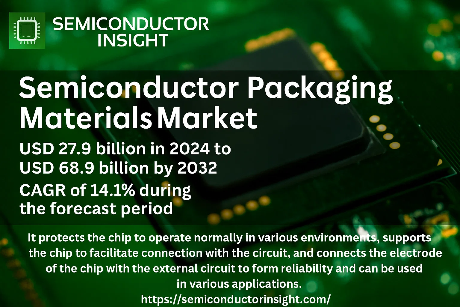
Global Semiconductor Packaging Materials Market was valued at USD 27.9 billion in 2024 to USD 68.9 billion by 2032, exhibiting a CAGR of 14.1% during the forecast period.
Semiconductor packaging has four main functions: protection, support, connection and reliability. It protects the chip to operate normally in various environments, supports the chip to facilitate connection with the circuit, and connects the electrode of the chip with the external circuit to form reliability and can be used in various applications.
The market is experiencing rapid growth due to several factors, including increased demand for advanced electronics, the proliferation of artificial intelligence (AI) and the Internet of Things (IoT), and the ongoing miniaturization of semiconductor devices. Additionally, the growing demand for high-performance computing and data centers is contributing to market expansion. The increasing adoption of electric vehicles and advanced driver-assistance systems (ADAS) is also expected to fuel the market growth. For instance, the global electric vehicle market is projected to reach 26.9 million units by 2030, according to the International Energy Agency (IEA). Key players in the market include Kyocera, Shinko, and Ibiden, among others.
MARKET DRIVERS
Proliferation of Advanced Electronics and Miniaturization
The relentless demand for smaller, faster, and more powerful electronic devices is a primary driver. The transition to advanced packaging technologies like Fan-Out Wafer-Level Packaging (FOWLP) and 2.5D/3D IC integration requires sophisticated materials, including advanced mold compounds, substrates, and thermal interface materials, to manage heat and ensure reliability in compact form factors.
Growth in Automotive and High-Performance Computing
The automotive sector’s shift towards electrification and autonomous driving, coupled with the exponential growth in data centers and AI workloads, creates robust demand for robust semiconductor packaging. Materials that offer high thermal conductivity, superior electrical performance, and exceptional reliability under harsh conditions are seeing increased adoption, with the automotive segment projected to be one of the fastest-growing.
➤ The global semiconductor packaging materials market is projected to exceed $30 billion by 2028, driven by these technological advancements.
Furthermore, the rise of the Internet of Things (IoT) and 5G infrastructure necessitates packaging solutions that are not only miniaturized but also cost-effective for mass production, fueling innovation in epoxy molding compounds, leadframes, and underfill materials.
MARKET CHALLENGES
Intense Cost and Supply Chain Pressures
The semiconductor packaging materials market faces significant margin pressure from the high cost of raw materials, including specialty resins, high-purity metals, and ceramics. Fluctuations in the supply of key materials and geopolitical trade tensions can lead to price volatility and supply chain disruptions, impacting production schedules for packaging and testing service providers.
Other Challenges
Technical Complexity of Advanced Nodes
As semiconductor nodes shrink to 5nm and below, packaging materials must meet extremely stringent requirements for low dielectric constant, low loss, and minimal coefficient of thermal expansion mismatch. Developing and qualifying these materials involves substantial R&D investment and lengthy validation cycles with chip manufacturers.
Environmental and Regulatory Hurdles
Increasingly stringent environmental regulations, such as restrictions on hazardous substances (RoHS) and REACH, require material suppliers to develop greener alternatives. This adds complexity and cost to the development of new packaging materials that are both high-performance and compliant.
MARKET RESTRAINTS
High Capital Investment for Material Innovation
The development of next-generation packaging materials, such as those for heterogeneous integration, requires substantial capital expenditure in specialized R&D facilities and manufacturing equipment. This high barrier to entry can restrain smaller players from competing effectively and slow down the pace of widespread material innovation across the industry.
Cyclical Nature of the Semiconductor Industry
The inherent cyclicality of the semiconductor market, characterized by periods of oversupply and demand contraction, directly impacts the packaging materials segment. During downturns, reduced chip production volumes lead to lower demand for packaging materials, creating uncertainty and affecting the financial stability of material suppliers.
MARKET OPPORTUNITIES
Expansion into Emerging Applications
Emerging applications in artificial intelligence, machine learning, and quantum computing present significant growth avenues. These high-performance computing applications demand packaging solutions with exceptional thermal management and signal integrity, opening opportunities for novel materials like silicon carbide substrates, glass cores, and advanced thermal interface materials.
Development of Sustainable and High-Performance Materials
There is a growing opportunity to develop sustainable packaging materials that reduce environmental impact without compromising performance. Bio-based epoxy molding compounds, halogen-free flame retardants, and recyclable substrates are areas of active development, driven by both regulatory demands and corporate sustainability goals from major OEMs.
Adoption of Chiplet-Based Architectures
The industry’s shift towards chiplet-based designs, which use multiple smaller dies in a single package, creates a substantial opportunity for materials used in die-to-die interconnects and high-density substrates. This trend is expected to drive demand for specialized underfills, adhesives, and substrate materials optimized for heterogenous integration.
Semiconductor Packaging Materials Market Trends
Robust Market Expansion Driven by Advanced Electronics
The global Semiconductor Packaging Materials market, valued at $27,990 million in 2024, is on a strong growth trajectory, projected to reach $68,900 million by 2032, representing a compound annual growth rate (CAGR) of 14.1%. This expansion is fundamentally supported by the critical role of packaging materials in ensuring the protection, support, connection, and reliability of semiconductor chips. The swift recovery in the broader semiconductor industry, with global sales expected to grow by 16% in 2024 after a 9.4% decline in 2023, directly fuels demand for advanced packaging solutions.
Other Trends
Demand for Advanced Substrates and High-Performance Resins
The market is witnessing a significant trend towards the adoption of sophisticated packaging substrates and encapsulating resins. As semiconductor devices become more powerful and compact, particularly for applications in artificial intelligence (AI), the Internet of Things (IoT), and high-performance computing, the demand for materials that offer superior thermal management, electrical performance, and miniaturization capabilities is intensifying. Packaging substrates and advanced resins are critical for enabling the faster processing times required to handle large data volumes in data centers and next-generation consumer electronics.
Geographical Shifts and Competitive Landscape
The Asia-Pacific region remains the dominant force in the Semiconductor Packaging Materials market, driven by high concentrations of semiconductor fabrication and assembly operations. Leading companies such as Kyocera, Shinko, and Ibiden, which collectively hold over 22% of the global market share, are heavily invested in this region. The continuous growth in consumer electronics consumption globally, coupled with the automotive sector’s increasing semiconductor content, ensures a sustained and diversified demand for packaging materials across various applications, including communications and medical devices. The competitive landscape is characterized by innovation aimed at meeting the stringent requirements of advanced semiconductor packages.
COMPETITIVE LANDSCAPE
Key Industry Players
Global Market Dominated by Japanese Specialists and Asian Manufacturing Giants
The global Semiconductor Packaging Materials market is moderately concentrated, with the top three companies—Kyocera, Shinko, and Ibiden—collectively holding over 22% of the market share. These leading players are primarily Japanese companies with deep expertise in advanced ceramic packaging substrates and high-density interconnect (HDI) substrates, which are critical for modern chip packaging. Their dominance is built on long-standing relationships with major semiconductor manufacturers, significant R&D investments in materials science, and sophisticated manufacturing capabilities for next-generation packaging technologies like fan-out wafer-level packaging (FO-WLP) and 2.5D/3D integration. The competitive environment is characterized by a continuous push for innovation to support the increasing performance and miniaturization demands of semiconductors used in AI, high-performance computing, and 5G applications.
Beyond the top tier, the market features a diverse array of significant players specializing in various material segments. Companies like Unimicron Technology, ZhenDing Tech, and Semco are major forces in the packaging substrate segment. In critical areas such as bonding wires, key suppliers include Tanaka and MK Electron, while encapsulating resins and die attach materials are dominated by specialists like Henkel and Hitachi Chemical. Furthermore, established giants like LG Innotek and Sumitomo provide a broad portfolio of materials, leveraging their scale and vertical integration. Niche players also hold important positions, such as Heraeus in precious metal bonding wires and Shin-Etsu in molding compounds, catering to specific high-reliability applications in automotive and medical electronics. This landscape ensures robust competition across different material types and geographic regions, particularly in the high-growth Asia-Pacific market.
List of Key Semiconductor Packaging Materials Companies Profiled
- Kyocera
- Shinko
- Ibiden
- LG Innotek
- Unimicron Technology
- ZhenDing Tech
- Semco
- KINSUS INTERCONNECT TECHNOLOGY
- Nan Ya PCB
- Nippon Micrometal Corporation
- Simmtech
- Mitsui High-tec, Inc.
- HAESUNG
- Shin-Etsu
- Heraeus
- Henkel
Segment Analysis:
| Segment Category | Sub-Segments | Key Insights |
| By Type |
|
Packaging Substrate consistently leads the market as it serves as the foundational platform for chip interconnections, with demand driven by the complexity of advanced IC designs. The crucial function of providing mechanical support and electrical connectivity makes it indispensable, particularly for high-performance computing and miniature devices. Innovations in substrate technologies are central to enabling next-generation packaging solutions that meet the stringent requirements for heat dissipation and signal integrity. |
| By Application |
|
Consumer Electronics is the dominant application segment, propelled by the massive global consumption of smartphones, tablets, and personal computers which rely heavily on advanced semiconductor packaging. The continuous demand for smaller, more powerful, and energy-efficient devices fuels innovation in packaging materials to enhance performance and reliability. This segment’s leadership is further reinforced by the rapid integration of AI and IoT capabilities into everyday consumer products. |
| By End User |
|
Integrated Device Manufacturers (IDMs) represent a leading segment due to their vertically integrated model that controls the entire production process from design to packaging. This end-user group demands highly specialized and reliable materials to maintain the quality and performance of their branded semiconductor products. The rigorous quality standards and the drive for product differentiation create a consistent and sophisticated demand for advanced packaging materials. |
| By Material Technology |
|
Organic Substrates are the leading material technology, favored for their cost-effectiveness, versatility, and suitability for high-volume manufacturing of a wide range of semiconductor devices. Their adaptability to complex circuitry designs and compatibility with surface-mount technology makes them a cornerstone of modern electronics packaging. The ongoing trend towards miniaturization and higher I/O density particularly benefits this technology segment. |
| By Packaging Platform |
|
Flip-Chip packaging remains the leading platform due to its superior electrical performance, high I/O density, and excellent thermal management characteristics compared to traditional wire bonding. Its dominance is underpinned by widespread adoption in high-performance applications such as processors, graphics chips, and networking equipment. The platform’s scalability and compatibility with advanced node technologies ensure its continued leadership in addressing the performance demands of next-generation electronics. |
Regional Analysis: Semiconductor Packaging Materials Market
The region’s dominance is anchored by its dense ecosystem of OSAT providers and leading-edge foundries. This concentration fosters a highly competitive environment where material suppliers must continuously innovate to meet the stringent performance and reliability requirements for packaging high-performance computing, smartphones, and automotive chips, creating a vibrant and demanding market for advanced materials.
Significant capital is being invested in developing next-generation packaging technologies. This focus drives demand for novel materials with specific properties, such as low dielectric constant substrates for high-speed signaling and advanced thermal management materials to dissipate heat from densely packed chips, positioning the region at the forefront of packaging material innovation.
The region benefits from a deeply integrated supply chain for materials, from basic chemicals to finished packaging substrates. This integration reduces costs, shortens lead times, and allows for close collaboration between material suppliers and packaging houses, enabling rapid iteration and customization of materials to suit specific application needs and accelerating time-to-market.
National policies, particularly in China, aimed at strengthening domestic semiconductor capabilities are a major market driver. These initiatives provide subsidies and create demand for locally sourced packaging materials, encouraging the growth of domestic material suppliers and reducing reliance on imports, which is reshaping the regional competitive landscape.
North America
North America’s market is characterized by strong demand driven by leading fabless semiconductor companies and high-performance computing applications. The region’s strength lies in its innovation-centric ecosystem, with significant research activities in next-generation packaging architectures like heterogeneous integration. Demand is particularly high for materials that enable superior electrical performance, thermal management, and reliability for data center, AI, and automotive semiconductors. The presence of major technology firms and a focus on cutting-edge applications creates a premium market segment for high-value, specialized packaging materials. Collaboration between material science companies, national labs, and chip designers fosters a pipeline of advanced material solutions tailored for the most demanding computing environments.
Europe
The European market for semiconductor packaging materials is driven by its strong automotive and industrial electronics sectors, which demand high reliability and longevity. There is a significant focus on materials that meet stringent automotive-grade qualifications for temperature cycling, moisture resistance, and long-term stability. The region also shows growing activity in power electronics and medical devices, requiring specialized packaging materials. European companies and research institutes are actively involved in developing sustainable and environmentally friendly material alternatives, aligning with the region’s strong regulatory focus. Collaboration within pan-European research initiatives supports innovation in materials for specialized applications beyond consumer electronics.
South America
The South American market for semiconductor packaging materials is nascent but developing, primarily driven by the consumer electronics and automotive industries in countries like Brazil. The market is characterized by a reliance on imported materials, with local demand focused on more mature, cost-effective packaging technologies. Growth is gradual, supported by regional economic development and increasing electronics manufacturing. The market dynamics are influenced by regional trade policies and the presence of multinational electronics assembly operations. There is potential for growth as the industrial base expands, but the region remains a relatively small player in the global landscape focused on standard material requirements.
Middle East & Africa
This region represents an emerging market with growth potential linked to strategic investments in technology and diversification efforts, particularly in Gulf Cooperation Council countries. The current demand for semiconductor packaging materials is limited but is expected to grow with new semiconductor fabrication projects and technology hubs. The focus is initially on establishing a basic electronics manufacturing infrastructure, which will drive demand for foundational packaging materials. Long-term growth will depend on the success of these diversification initiatives and the development of local technology ecosystems, with the market currently served predominantly by international material suppliers.
Report Scope
This market research report provides a comprehensive analysis of the Semiconductor Packaging Materials Market , covering the forecast period 2025–2032. It offers detailed insights into market dynamics, technological advancements, competitive landscape, and key trends shaping the industry.
Key focus areas of the report include:
- Market Overview: The report begins with an overview outlining its current market scenario, key growth indicators, and industry transformation drivers. It discusses macroeconomic factors, demand–supply balance, regulatory landscape, and the strategic role of semiconductors in powering advancements across industries such as automotive, telecommunications, consumer electronics, and industrial automation.
- Market Size & Forecast: Historical data and future projections for revenue, unit shipments, and market value across major regions and segments.
- Segmentation Analysis: Detailed breakdown by product type, technology, application, and end-user industry to identify high-growth segments and investment opportunities.
- Regional Insights: Insights into market performance across North America, Europe, Asia-Pacific, Latin America, and the Middle East & Africa, including country-level analysis where relevant.
- Competitive Landscape: Profiles of leading market participants, including their product offerings, R&D focus, manufacturing capacity, pricing strategies, and recent developments such as mergers, acquisitions, and partnerships.
- Technology Trends & Innovation: Assessment of emerging technologies, integration of AI/IoT, semiconductor design trends, fabrication techniques, and evolving industry standards.
- Market Drivers & Restraints: Evaluation of factors driving market growth along with challenges, supply chain constraints, regulatory issues, and market-entry barriers.
- Stakeholder Insights: Insights for component suppliers, OEMs, system integrators, investors, and policymakers regarding the evolving ecosystem and strategic opportunities.
Primary and secondary research methods are employed, including interviews with industry experts, data from verified sources, and real-time market intelligence to ensure the accuracy and reliability of the insights presented.
FREQUENTLY ASKED QUESTIONS:
What is the current market size of Semiconductor Packaging Materials Market?
-> Semiconductor Packaging Materials Market was valued at USD 27.9 billion in 2024 to USD 68.9 billion by 2032, exhibiting a CAGR of 14.1% during the forecast period.
Which key companies operate in Semiconductor Packaging Materials Market?
-> Key players include Kyocera, Shinko, Ibiden, LG Innotek, and Unimicron Technology, among others. Global top three companies hold a share over 22%.
What are the key growth drivers?
-> Key growth drivers include the growing global consumer electronics consumption, development of artificial intelligence (AI), the Internet of Things (IoT), and machine learning (ML) technologies, and rising demand for faster and more advanced memory chips in data center applications.
Which region dominates the market?
-> Asia is a dominant region in the market, with key segments including China, Japan, South Korea, and Southeast Asia.
What are the emerging trends?
-> Emerging trends include the integration of AI/IoT technologies to enhance memory chip processing, fabrication techniques, and evolving industry standards for semiconductor reliability and performance.

Get Sample Report PDF for Exclusive Insights
Report Sample Includes
- Table of Contents
- List of Tables & Figures
- Charts, Research Methodology, and more...