Package Substrates Market Insights
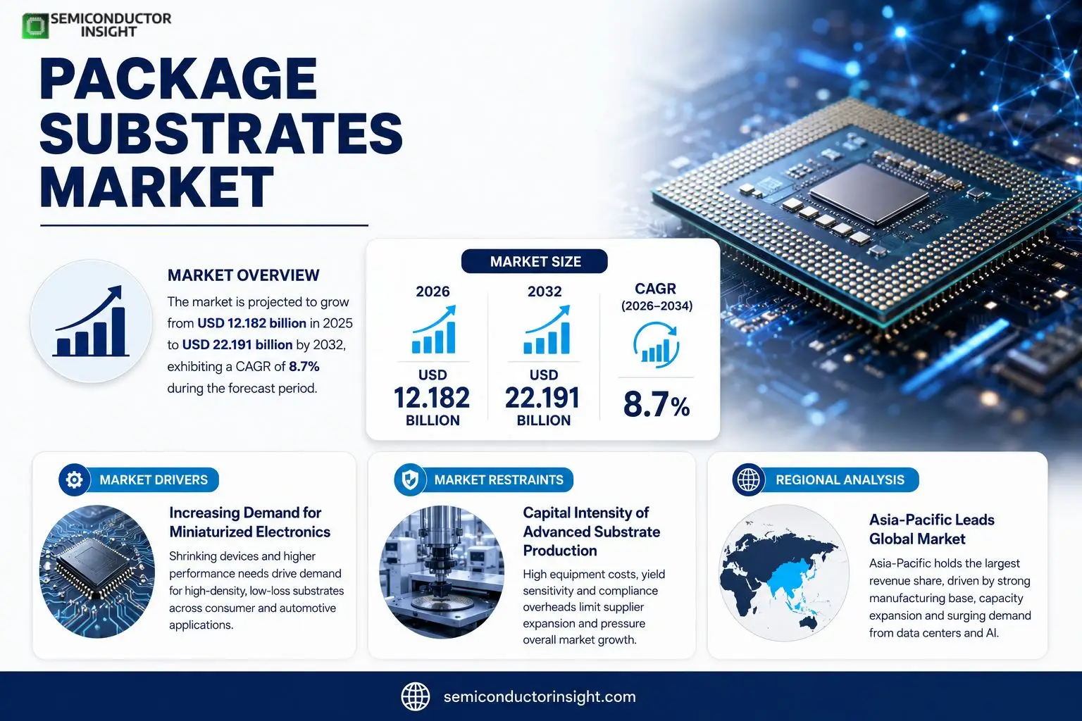
Package Substrates market size was valued at USD 12.182 billion in 2026 to USD 22.191 billion by 2034, exhibiting a CAGR of 8.7% during the forecast period.
Package substrates are engineered interposers that connect semiconductor dies to printed circuit boards, delivering electrical interconnection, power distribution, signal routing, thermal management and mechanical support. Major product families include high‑end FCBGA for HPC and server CPUs/GPUs, FCCSP for mobile processors and consumer electronics, and WB‑BGA for lower‑pin‑count or memory modules.The market is expanding because data‑center compute demand fuels larger, multilayer ABF build‑up substrates, while the rollout of AI accelerators pushes tighter line‑space requirements. Simultaneously, mobile and wearable segments sustain volume growth for FCCSP offerings. Leading manufacturers such as Unimicron, Ibiden and Nan Ya PCB are scaling capacity in Taiwan (28 % share), South Korea (27 %) and Mainland China (22 %), reinforcing supply resilience amid rising component complexity.
MARKET DRIVERS
Increasing Demand for Miniaturized Electronics
Package Substrates Market is being pulled forward by the relentless push toward smaller, lighter devices in consumer and automotive sectors. As chip footprints shrink, manufacturers require substrates that can accommodate tighter pitch interconnects while maintaining thermal stability. This technical imperative forces suppliers to innovate, opening up revenue streams for firms that can deliver high‑density, low‑loss materials.
Growth of Advanced Packaging Technologies
Emerging packaging formats such as fan‑out wafer‑level packaging (FO‑WLP) and system‑in‑package (SiP) place new performance criteria on substrates, especially regarding signal integrity and mechanical robustness. Companies that align their product roadmaps with these formats capture a larger share of Package Substrates Market, because end‑users are willing to pay a premium for reliability in high‑frequency applications.
➤ Customers are shifting budgets from traditional PCB purchases to specialty substrate solutions that enable higher functionality per unit volume.
Regulatory pressures around environmental compliance also accelerate the transition toward lead‑free and recyclable substrate chemistries. Vendors that embed sustainable practices into their manufacturing lines not only meet tightening legislation but also differentiate themselves to OEMs that are under increasing ESG scrutiny.
MARKET CHALLENGES
Supply‑Chain Volatility
Fluctuations in raw‑material availability, particularly high‑purity copper and advanced polymer resins, create cost uncertainty for Package Substrates Market. When a single supplier faces geopolitical constraints, downstream manufacturers experience lead times that jeopardize product launch schedules.
Other Challenges
Design complexity is rising faster than the industry’s ability to standardize testing protocols. Engineers must validate thermal cycling, moisture resistance, and electrical performance for each new substrate iteration, which inflates development budgets and slows time‑to‑market.
Technology Adoption Lag
Some legacy OEMs hesitate to migrate from conventional FR‑4 boards to newer substrate platforms due to perceived integration risk. This inertia caps overall market expansion until convincing case studies demonstrate clear ROI.
MARKET RESTRAINTS
Capital Intensity of Advanced Substrate Production
Establishing a line capable of handling sub‑micron feature sizes demands multi‑million‑dollar investments in cleanroom facilities, precision lithography, and in‑line metrology. Smaller players often lack the financial muscle to compete, which narrows the competitive field and limits price elasticity.Furthermore, high‑volume manufacturing of specialty substrates suffers from yield sensitivity; even minor process deviations can translate into substantial scrap rates. This risk deters some investors from committing capital to expansion projects, thereby tempering the overall growth trajectory of Package Substrates Market.The regulatory landscape for chemical usage in substrate fabrication continues to tighten. Compliance testing adds overhead, and non‑conformity can result in costly product recalls, reinforcing a conservative approach among manufacturers.
MARKET OPPORTUNITIES
Emergence of 5G and Edge Computing
5G infrastructure and edge‑computing nodes demand substrates that can support higher data rates and greater thermal loads. Companies that tailor their material formulations to these exacting specifications are positioned to win contracts from telecom equipment makers and data‑center providers, expanding the addressable market.Another fertile avenue lies in the automotive electrification trend. Electric vehicles and advanced driver‑assistance systems (ADAS) rely on densely packed sensor arrays, which in turn require robust high‑frequency substrates. Early entrants that secure certification for automotive safety standards can lock in long‑term supply agreements.Finally, the rise of additive manufacturing for electronic components opens a niche for customized, on‑demand substrates. By integrating digital design workflows with rapid prototyping, suppliers can offer low‑volume, high‑mix solutions that were previously unprofitable, thereby creating a new revenue stream within Package Substrates Market.
Package Substrates Market Trends
Rise of High‑Pin‑Count ABF Substrates for AI and Data‑Center Compute
Package Substrates Market is witnessing a decisive shift toward advanced build‑up film (ABF) platforms that support far more interconnect layers than legacy solutions. Data‑center processors and AI accelerators demand socket‑level bandwidth that only dense, low‑loss ABF stacks can deliver, prompting chip designers to specify FCBGA architectures with pin counts exceeding several thousand. This technical imperative has amplified orders for multi‑layer substrates from the core East‑Asian manufacturers, whose capacity expansions are now tied to multi‑year qualification roadmaps rather than short‑term sales cycles. As a result, utilization rates at the largest Taiwanese and Korean fabs frequently operate above ninety percent, while suppliers are locking in long‑term material contracts to safeguard against volatility in copper foil and specialty dielectric supply.
Other Trends
Material Innovation: From BT Resins to Glass‑Core Platforms
Beyond sheer density, the substrate value chain is being reshaped by a wave of material upgrades. BT resin systems, once the default for mainstream mobile packages, are increasingly supplemented by glass‑core constructions that offer superior dimensional stability and reduced thermal expansion. This transition matters because emerging 2.5D and 3D integration schemes rely on exact line‑spacing and minimal warpage to maintain signal integrity at terabit‑per‑second data rates. Early adopters such as leading OSATs have already qualified glass‑core panels for high‑performance networking chips, signalling a broader industry move away from purely polymer‑based cores. The material shift also introduces new competitive dynamics for dielectric suppliers, who must now invest in low‑loss silicate chemistries to stay relevant.
Supply‑Chain Realignment and Regional Diversification
Geopolitical considerations are prompting a gradual rebalancing of Package Substrates Market’s supply network. While East Asia continues to host over seventy‑seven percent of revenue, policy incentives in North America and Europe are encouraging pilot lines for glass‑core and silicon‑interposer technologies. These initiatives reduce reliance on a single manufacturing basin and open avenues for domestic OEMs to source critical interconnect components closer to their assembly plants. For manufacturers, the emerging regional footprints present both risk mitigation opportunities and strategic differentiation, as customers increasingly prefer suppliers who can demonstrate resilient, multi‑region delivery capabilities. In the medium term, this diversification is likely to ease material bottlenecks and foster a more competitive pricing environment across the substrate ecosystem.
COMPETITIVE LANDSCAPEKey Industry Players
Package Substrates Competitive Overview – 2024
Unimicron, Ibiden and Nan Ya PCB jointly command a commanding share of the package‑substrate arena, together accounting for roughly three‑quarters of worldwide revenue in 2024. Their dominance stems from deep integration across the ABF and BT value chains, extensive capacity in high‑layer‑count builds, and long‑standing relationships with leading chip designers such as Intel, AMD and NVIDIA. The concentration of production in Taiwan, South Korea and Japan reinforces a supply network that can quickly scale for data‑center and AI workloads while maintaining tight tolerances required by advanced packaging formats. Market structure therefore resembles a tiered oligopoly: the top tier supplies the majority of high‑end FCBGA and FCCSP volumes, the mid‑tier focuses on mid‑range WB‑BGA and memory‑oriented substrates, and a broader fringe of regional manufacturers addresses niche automotive and consumer segments.Beyond the headline firms, a cadre of specialized players adds depth to the ecosystem. Companies such as AT&S, Samsung Electro‑Mechanics and Kyocera provide critical BT‑resin and copper‑foil expertise that underpins mainstream mobile and consumer products. Emerging capacity from Zhen Ding Technology, Daeduck Electronics and Shennan Circuit illustrates a strategic push to capture growing demand for 2.5D/3D integration and high‑bandwidth memory modules. Meanwhile, firms like LG InnoTek and Korea Circuit are expanding glass‑core and MIS substrate lines, positioning themselves for the next wave of high‑density interconnects. This mixture of established scale players and agile innovators creates a competitive dynamic where technology leadership, material sourcing reliability and geographic proximity to OSATs become decisive factors for customer selection.
List of Key Package Substrates Companies Profiled
- Unimicron
- Ibiden
- Nan Ya PCB
- Shinko Electric Industries
- Kinsus Interconnect Technology
- AT&S
- Samsung Electro‑Mechanics
- Kyocera
- Toppan
- Zhen Ding Technology
- Daeduck Electronics
- Zhuhai Access Semiconductor
- LG InnoTek
- Shennan Circuit
- Shenzhen Fastprint Circuit Tech
Segment Analysis:
| Segment Category | Sub-Segments | Key Insights |
| By Type |
|
FCBGA Substrate is the primary driver for high‑performance computing packages.
|
| By Application |
|
Data Center / Server applications dominate substrate demand.
|
| By End User |
|
Server OEMs shape the high‑end substrate roadmap.
|
| By Material |
|
ABF Dielectric Build‑up is the strategic material for future‑proof packaging.
|
| By Technology |
|
Chiplet Integration acts as the next substrate frontier.
|
Regional Analysis: Package Substrates Market
Leading substrate manufacturers in North America are shifting toward low‑k dielectric films and copper‑clad laminates to meet thermal‑budget constraints. This migration reflects a strategic response to the escalating power density of AI‑focused processors, where substrate thermal performance has become a decisive factor for product qualification.
End‑to‑end visibility is now a priority, prompting OEMs to embed substrate sourcing within broader procurement platforms. The resulting integration trims lead times and buffers against geopolitical shocks that could otherwise disrupt material availability.
Universities in the Midwest and research labs on the West Coast have forged consortia that pool funding and expertise, accelerating the validation of high‑frequency substrate prototypes tailored for 5G and edge‑compute devices.
Recent revisions to environmental compliance standards encourage the adoption of greener substrate chemistries, prompting firms to redesign processes that reduce volatile organic compound emissions without compromising yield.
Europe
European players are leveraging a strong legacy in precision engineering to specialize in high‑reliability package substrates for aerospace and medical applications. The region’s emphasis on sustainability has spurred early trials of bio‑based resin systems, positioning Europe as a testbed for environmentally conscious substrate solutions. Collaborative frameworks between Germany’s industrial clusters and Nordic research institutes foster rapid iteration cycles, enabling niche market entrants to address stringent certification requirements that customers increasingly demand.
Asia-Pacific
Asia‑Pacific exhibits the most rapid shift in demand volume, driven by the proliferation of consumer electronics manufacturing hubs in China, South Korea, and Taiwan. Local substrate suppliers are scaling capacity through joint ventures that combine capital intensity with advanced process know‑how, often under the guidance of government incentives aimed at bolstering semiconductor self‑sufficiency. This aggressive expansion is tempered by talent shortages in high‑complexity substrate design, prompting firms to import expertise from established North American and European R&D centers.
South America
In South America, Brazil’s modest but growing semiconductor ecosystem is beginning to explore package substrate opportunities as part of a broader diversification away from commodity commodities. Public‑private partnerships are funding pilot lines that test substrate compatibility with emerging flexible display technologies, a segment that could unlock export potential to neighboring markets seeking cost‑effective alternatives to traditional rigid packages.
Middle East & Africa
The Middle East & Africa region remains in an exploratory phase, with UAE and Israel leading niche research into high‑temperature substrate materials suitable for harsh‑environment oil‑field electronics. While volume remains limited, strategic investments in test facilities hint at a long‑term ambition to develop a regional value chain that can service both local energy projects and international aerospace contracts.
Report Scope
This market research report provides a comprehensive analysis of Package Substrates Market, covering the forecast period 2026–2034. It offers detailed insights into market dynamics, technological advancements, competitive landscape, and key trends shaping the industry.
Key focus areas of the report include:
- Market Overview: The report begins with an overview outlining its current market scenario, key growth indicators, and industry transformation drivers. It discusses macroeconomic factors, demand–supply balance, regulatory landscape, and the strategic role of semiconductors in powering advancements across industries such as automotive, telecommunications, consumer electronics, and industrial automation.
- Market Size & Forecast: Historical data and future projections for revenue, unit shipments, and market value across major regions and segments.
- Segmentation Analysis: Detailed breakdown by product type, technology, application, and end-user industry to identify high-growth segments and investment opportunities.
- Regional Insights: Insights into market performance across North America, Europe, Asia-Pacific, Latin America, and the Middle East & Africa, including country-level analysis where relevant.
- Competitive Landscape: Profiles of leading market participants, including their product offerings, R&D focus, manufacturing capacity, pricing strategies, and recent developments such as mergers, acquisitions, and partnerships.
- Technology Trends & Innovation: Assessment of emerging technologies, integration of AI/IoT, semiconductor design trends, fabrication techniques, and evolving industry standards.
- Market Drivers & Restraints: Evaluation of factors driving market growth along with challenges, supply chain constraints, regulatory issues, and market-entry barriers.
- Stakeholder Insights: Insights for component suppliers, OEMs, system integrators, investors, and policymakers regarding the evolving ecosystem and strategic opportunities.
Primary and secondary research methods are employed, including interviews with industry experts, data from verified sources, and real-time market intelligence to ensure the accuracy and reliability of the insights presented.
FREQUENTLY ASKED QUESTIONS:
What is the current market size of Package Substrates Market?
-> Package Substrates market size was valued at USD 12.182 billion in 2026 to USD 22.191 billion by 2034, exhibiting a CAGR of 8.7% during the forecast period
Which key companies operate in Package Substrates Market?
-> Key players include Unimicron, Ibiden, Nan Ya PCB, Shinko Electric Industries, Kinsus Interconnect Technology, AT&S, Samsung Electro-Mechanics, Kyocera, Toppan, among others.
What are the key growth drivers?
-> Key growth drivers include explosive demand for high‑performance computing, AI accelerators, data‑center servers, advanced packaging technologies such as 2.5D/3D integration, and the shift toward higher‑layer‑dense ABF substrates.
Which region dominates the market?
-> Asia (particularly Taiwan, South Korea, China Mainland, and Japan) dominates both production capacity and revenue share in Package Substrates Market.
What are the emerging trends?
-> Emerging trends include chiplet‑centric advanced packaging, 2.5D/3D integration, high‑bandwidth memory (HBM) ecosystems, glass‑core substrate development, and semi‑additive process innovations for higher routing density.
Get Sample Report PDF for Exclusive Insights
Report Sample Includes
- Table of Contents
- List of Tables & Figures
- Charts, Research Methodology, and more...