Key Statistics
Key Takeaways
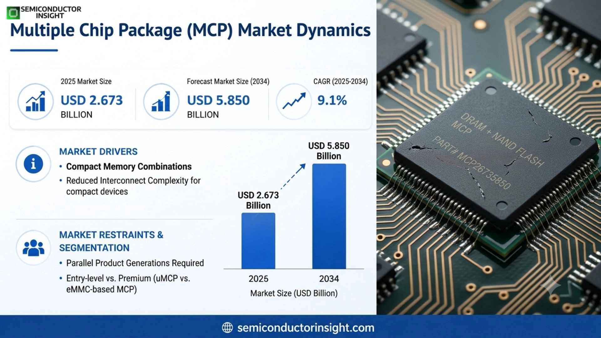
- Global Multiple Chip Package (MCP) Market reaches approximately USD 2.673 billion in 2025 and USD 5.850 billion by 2034, maintaining the 9.1% growth trajectory implied by the published 2024 and 2030 market anchors. Demand is concentrated in compact memory combinations that integrate DRAM with NAND or managed storage inside one package, reducing board area and interconnect complexity for smartphones, edge devices, industrial electronics and connected systems.
- UFS-based MCP, commonly called uMCP, is the highest-performance growth segment because it combines low-power DRAM with UFS storage for bandwidth-intensive mobile and edge workloads. Micron states that its uMCP5 platform can support 6.4 Gb/s DRAM bandwidth, roughly double UFS 3.1 sequential-read performance versus UFS 2.1 and nearly half the footprint of discrete memory solutions. Samsung likewise positions uMCP for 5G, AI and compact edge-device designs.
- Asia Pacific is the largest market because the region contains the dominant memory manufacturing, semiconductor assembly and smartphone electronics supply chains. Samsung, Winbond, Macronix and Dosilicon are headquartered in Asia, while major outsourced semiconductor packaging and device manufacturing is concentrated across South Korea, China, Taiwan and Southeast Asia. SIA reported that Asia Pacific/All Other semiconductor sales increased 45.0% in 2025, strengthening the region’s role as both a production and consumption center.
- The market’s commercial challenge is that MCP economics depend on the simultaneous availability and qualification of multiple memory dies, package substrates, assembly processes and end-system interfaces. A shortage or yield issue in one component can constrain the full package even when the other die is available. This makes known-good-die testing, package-level reliability, thermal behavior and long-term supply agreements central to supplier selection, particularly in industrial and automotive applications with longer qualification cycles.
Global Multiple Chip Package (MCP) Market Overview
A Multiple Chip Package integrates two or more semiconductor dies within a single package to reduce footprint, simplify printed-circuit-board design and combine complementary functions. In the controlling report scope, MCP products are divided into e.MMC-Based MCP, UFS-Based MCP or uMCP, and NAND-Based MCP. Applications span Electronic Products, Industrial Manufacture, Medical Industry, Communications Industry and Other uses, so the market includes both high-volume mobile memory packages and specialized embedded memory combinations.
The strongest commercial value proposition is board-space reduction without forcing the customer to redesign every memory interface separately. Samsung’s eMCP combines LPDDR4X DRAM with eMMC 5.1 storage for entry and mainstream mobile devices, while Micron’s uMCP combines LPDDR memory and UFS storage for higher-performance platforms. Infineon extends the MCP concept beyond mobile memory by combining flash and RAM and by supplying known-good wafer or die formats for custom system-in-package and multi-chip-package designs.
MCP product design must balance electrical performance, power, thermals, package height, memory density and interface compatibility. Mobile packages favor extremely small footprints and low power, while industrial designs value long product availability, high-temperature screening and standardized interfaces. This diversity makes the market broader than smartphone memory alone. It also explains why suppliers compete through package architecture, die qualification, interface roadmaps and lifecycle support rather than simply through raw NAND or DRAM capacity.
Segment Analysis: By Type
| Type | Market interpretation |
|---|---|
| e.MMC-Based MCP | e.MMC-based MCP combines low-power DRAM with managed eMMC storage in one package and remains important for entry-level and mainstream mobile or embedded designs where cost, simplicity and compactness matter more than maximum storage bandwidth. Samsung’s current eMCP portfolio uses LPDDR4X with eMMC 5.1, supports DRAM speeds up to 4,266 Mbps and offers multiple density combinations, illustrating the segment’s role as a cost-efficient integration platform for mature device tiers. |
| UFS-Based MCP (uMCP) | uMCP is the performance-led segment because UFS provides higher storage throughput than eMMC while retaining the footprint benefits of an integrated package. Micron’s uMCP5 supports up to 6.4 Gb/s DRAM bandwidth and uses UFS 3.1, while Samsung markets LPDDR5 uMCP for 5G and AI-enabled devices. Growth is strongest where mobile AI, high-resolution media and edge computing increase memory bandwidth and storage-performance requirements without expanding available board area. |
| NAND-Based MCP | NAND-based MCP pairs NAND flash with RAM or other memory components for embedded and communications applications that need compact, reliable nonvolatile storage. Micron offers NAND-based MCP with SLC NAND supporting high endurance, while Macronix has supplied NAND MCP solutions for LTE IoT chipsets and Dosilicon combines NAND Flash with multiple LPDDR generations. The segment is particularly relevant where long lifecycle, low power and embedded-system simplicity outweigh the need for the newest managed-storage interface. |
Segment Analysis: By Application
| Application | Demand characteristics |
|---|---|
| Electronic Products | Electronic products are the largest demand pool because smartphones, wearables, tablets and connected consumer devices face the strongest pressure to combine more memory with less board area. GSMA reported that 1.5 billion unique mobile-internet subscribers were using a 5G smartphone by 2025 reporting, while smartphone ownership reached 4.4 billion people. Higher 5G adoption, on-device AI and richer media workloads raise memory-performance requirements and favor integrated packages in cost- and space-sensitive designs. |
| Industrial Manufacture | Industrial equipment uses MCPs where controllers, HMIs, machine vision and connected edge systems require compact memory with long supply life and reliable operation. Infineon’s Flash+RAM MCP portfolio explicitly targets industrial HMI and machine-vision systems and emphasizes standardized xSPI interfaces, reduced PCB layers and faster time to market. Industrial demand is smaller than smartphones but commercially attractive because qualification is sticky and customers may prioritize lifecycle support and temperature performance over lowest unit cost. |
| Medical Industry | Medical devices increasingly integrate displays, connectivity, local data processing and embedded storage, creating opportunities for compact memory packages in portable diagnostic instruments, patient monitors and connected equipment. MCP adoption is strongest where product designers need to reduce board area while maintaining stable firmware and data storage. The qualification burden is higher than in consumer devices because product changes may require extensive verification, favoring suppliers with long-term availability programs and documented reliability screening. |
| Communications Industry | Communications applications include routers, gateways, modems, small cells and connected IoT platforms that need embedded flash plus working memory. Macronix previously qualified NAND MCP with a Qualcomm LTE IoT chipset, demonstrating the architecture’s fit for compact communications modules. As 5G connections expand, the addressable installed base of edge connectivity equipment rises, but design wins depend on chipset compatibility, interface standards, power budgets and the ability to maintain package supply through long equipment lifecycles. |
| Other | Other MCP applications span automotive electronics, security systems, smart-home products and specialized embedded devices. Micron highlights multichip-package memory for next-generation connected vehicles, while Infineon offers known-good die for custom MCP implementations. These applications often use lower volumes than smartphones but demand higher reliability and extended product support. Suppliers can therefore capture premium value where qualification, temperature screening and long-term continuity reduce the customer’s risk of redesigning an embedded platform. |
Regional Analysis
Asia Pacific is the largest MCP region because memory fabrication, semiconductor packaging and electronics assembly are concentrated across South Korea, China, Taiwan, Japan and Southeast Asia. North America is a major design and consumption market through smartphone platforms, cloud-connected devices, industrial electronics and semiconductor vendors such as Micron, Texas Instruments and Infineon’s U.S. customer ecosystem. Europe is strongest in industrial, automotive and communications uses, while South America and Middle East & Africa remain primarily downstream device markets served through imported memory packages.
| Region | Position | Growth outlook | Commercial basis |
|---|---|---|---|
| Asia Pacific | Largest | Strong | Memory manufacturing, smartphone assembly, IoT electronics and packaging concentration create the deepest regional MCP supply and customer ecosystem. |
| North America | High-value design market | Moderate to strong | Mobile platforms, embedded systems and industrial design centers create qualification demand even though much package manufacturing occurs in Asia. |
| Europe | Industrial and automotive market | Moderate | Long-lifecycle embedded systems and automotive electronics favor reliable flash-plus-RAM and known-good-die MCP architectures. |
| South America | Emerging downstream market | Gradual | Smartphone adoption, telecom upgrades and industrial electronics drive demand mainly through imported finished devices and modules. |
| Middle East & Africa | Emerging mobile and IoT market | Gradual to strong from low base | 5G expansion and smartphone replacement support memory demand while local MCP manufacturing remains limited. |
Asia Pacific
Asia Pacific combines the market’s strongest upstream and downstream positions. Samsung in South Korea, Winbond and Macronix in Taiwan and Dosilicon in China are part of the controlling company set, while the region also hosts extensive outsourced assembly and electronics manufacturing. GSMA reported that developed Asia Pacific and Greater China were already among the leading 5G adoption regions, increasing demand for memory bandwidth and storage density. This creates a market where MCP suppliers benefit from proximity to handset, module and embedded-equipment customers as well as packaging partners.
| Country / subregion | Commercial logic |
|---|---|
| China | Large smartphone, IoT and industrial-electronics production supports MCP consumption, while domestic memory suppliers such as Dosilicon broaden local sourcing options. |
| South Korea | Samsung’s integrated memory manufacturing and mobile-device ecosystem makes South Korea strategically important for both uMCP/eMCP production and qualification. |
| Taiwan & Southeast Asia | Taiwan contributes memory suppliers and packaging capability, while Southeast Asia hosts assembly and electronics manufacturing that supports regional supply-chain diversification. |
Dated market instances
North America
North America is commercially important because U.S. semiconductor and platform companies influence memory-interface standards and embedded-system design even when packages are assembled in Asia. Micron is a major MCP supplier, Texas Instruments participates in the controlling competitive scope, and Infineon supports custom MCP solutions through known-good wafer and die products. Mobile AI and edge computing also increase memory-performance requirements across devices designed for North American customers, making qualification relationships with chipset vendors and OEMs a key route to design wins.
| Country / subregion | Commercial logic |
|---|---|
| United States | Micron’s uMCP and multichip-package portfolio, combined with large mobile, industrial and communications design ecosystems, makes the U.S. the region’s core market. |
| Canada | Demand is concentrated in communications, embedded systems and industrial technology, typically supplied through global semiconductor channels. |
| Mexico | Electronics and automotive assembly create downstream demand for memory modules and MCP-enabled devices within North American manufacturing networks. |
Dated market instances
Europe
Europe’s MCP opportunity is led by industrial automation, automotive electronics and communications equipment rather than global smartphone assembly. Infineon offers Flash+RAM MCP and known-good-die solutions that emphasize standardized interfaces, longevity and high-temperature screening, characteristics that align with European industrial and automotive requirements. Customers often need product availability for a decade or longer, making qualification stability and lifecycle programs critical. This produces a slower-volume but higher-retention market than fast-turn consumer electronics.
| Country / subregion | Commercial logic |
|---|---|
| Germany | Industrial automation, automotive and embedded-system design create strong demand for long-lifecycle memory integration and high-reliability qualification. |
| France & Benelux | Communications, industrial and medical electronics support compact memory designs through global semiconductor distribution channels. |
| United Kingdom | Industrial and communications design activity creates selective MCP demand, particularly where board-space reduction and long-term memory availability are important. |
Dated market instances
South America
South America remains predominantly a downstream market for MCP-enabled smartphones, communications modules and industrial equipment. Brazil is the largest opportunity because it combines the region’s biggest electronics consumer base with local manufacturing and telecom investment. Direct memory-package fabrication is limited, so suppliers usually reach customers through global handset and module supply chains. Commercial growth therefore follows smartphone replacement, 4G-to-5G migration and imported industrial electronics rather than new local MCP factories.
| Country / subregion | Commercial logic |
|---|---|
| Brazil | Largest regional electronics market and the principal destination for MCP-enabled smartphones, telecom equipment and embedded products. |
| Argentina | Demand is mainly indirect through imported devices, industrial controls and communications equipment. |
| Rest of South America | Growth follows handset replacement, telecom modernization and adoption of connected industrial devices. |
Dated market instances
Middle East & Africa
Middle East & Africa offers a growing device-demand opportunity as 5G coverage expands in Gulf markets and smartphone ownership rises across emerging economies. Direct MCP manufacturing remains limited, so demand arrives through imported smartphones, IoT modules and industrial systems. The region contains very different technology profiles: GCC states are among the world’s fastest 5G adopters, while Sub-Saharan Africa retains a larger 2G and 3G device base. This supports both performance-oriented uMCP and lower-cost eMCP depending on country and device tier.
| Country / subregion | Commercial logic |
|---|---|
| GCC states | High 5G penetration and premium-device adoption favor UFS-based memory packages and higher DRAM densities. |
| South Africa | Enterprise, telecom and consumer-device demand supports MCP use through imported smartphones and connected equipment. |
| Sub-Saharan Africa | Large feature-phone and legacy-smartphone bases create a longer transition path where cost-efficient memory packages remain commercially important. |
Dated market instances
Key Multiple Chip Package (MCP) Manufacturers and Competitive Landscape
The competitive landscape is concentrated around memory manufacturers that can combine qualified DRAM and nonvolatile memory dies inside compact packages. Samsung and Micron have the broadest direct mobile MCP offerings, while Dosilicon and Macronix address embedded and IoT combinations. Infineon contributes Flash+RAM MCP and known-good-die products suited to industrial and custom packages, and Winbond remains an important specialty-memory supplier. Texas Instruments is retained in the controlling company scope, reflecting the report’s broader semiconductor-package competitive frame.
Design wins depend on more than memory density. Suppliers must coordinate DRAM speed, storage interface, package footprint, power, thermal behavior and compatibility with customer chipsets. Micron and Samsung differentiate through uMCP performance and compactness, while Infineon emphasizes standardized interfaces and long-term availability. This creates segmented competition: high-volume mobile devices reward density, speed and cost; industrial and medical systems place greater weight on qualification, lifecycle support and operating-temperature performance.
| Competitive role | Companies and positioning |
|---|---|
| Mobile memory integration leaders | Samsung and Micron Technology compete with eMCP/uMCP architectures that integrate low-power DRAM and managed storage for smartphones and edge devices. |
| Embedded and specialty memory suppliers | Dosilicon, Macronix and Winbond Electronics Corp address embedded, IoT and industrial memory demand with NAND, NOR and DRAM capabilities that can be combined in MCP architectures. |
| Industrial/custom package ecosystem | Infineon (Cypress) provides Flash+RAM MCP and known-good wafer/die solutions for custom MCP or SiP designs, while Texas Instruments is included in the controlling competitive scope through its broad embedded semiconductor and packaging presence. |
Companies covered in the report
- Dosilicon
- Samsung
- Texas Instruments
- Infineon (Cypress)
- Micron Technology
- Macronix
- Winbond Electronics Corp.
The complete controlling company set is retained for competitive profiling. Evaluation separates mobile uMCP and eMCP leaders from embedded-memory specialists and broader semiconductor participants. It compares DRAM and storage-interface combinations, known-good-die controls, package footprint, thermal behavior, chipset compatibility, lifecycle support and customer qualification. The seven companies are not treated as interchangeable because their product portfolios, target device tiers and exposure to smartphone, industrial or communications design cycles differ materially.
MCP Architecture, Die-Qualification and Package-Reliability Analysis
MCP production capacity depends on the availability of qualified DRAM, NAND or NOR die as well as assembly and final-test capacity. An integrated package cannot be produced at the desired mix if one die type is constrained, so memory-fab allocation directly affects package output. Known-good-die screening is especially important because combining several dies magnifies yield economics: a defective component can make the entire package unusable after assembly. Suppliers therefore balance die yields, package assembly throughput and end-customer forecasts across multiple density combinations.
Capacity flexibility is a competitive advantage because mobile demand shifts rapidly between memory densities and interface generations. Samsung and Micron can pair internal DRAM and NAND portfolios with package engineering, while smaller suppliers may rely more on selected die combinations or external assembly partners. Industrial MCP capacity is less volume-driven but requires stable long-term processes and qualification. Infineon’s known-good-wafer offering and longevity program illustrate how usable capacity is defined not simply by wafer starts but by tested, supported dies that can remain available across long embedded-product lifecycles.
Global Multiple Chip Package (MCP) Market Dynamics: Drivers, Restraints and Opportunities
The market is moving toward a two-tier structure. Premium and upper-mainstream mobile devices increasingly use faster UFS-based storage and higher-bandwidth low-power DRAM, which favors uMCP. Entry-level smartphones and many embedded devices still value the lower cost and mature ecosystem of eMMC-based MCP or NAND-plus-RAM combinations. Suppliers therefore need multiple product generations in parallel, because faster interfaces do not immediately replace mature packages in cost-sensitive markets, industrial platforms or regions where device replacement cycles are longer.
Memory-price cycles create another important dynamic. MCP suppliers purchase or internally allocate DRAM and NAND dies whose pricing can move rapidly with global supply-demand conditions. SIA reported strong memory-sales growth in 2025, while smartphone vendors also faced rising memory costs entering 2026. Higher die prices can lift package revenue but pressure OEM margins and slow upgrades in entry-level devices. Integrated suppliers with internal memory production may gain supply advantages, but they still must manage package mix and customer affordability.
MARKET DRIVERS
| Factor | Directional CAGR impact | Most exposed market | Time horizon |
|---|---|---|---|
| 5G and mobile AI memory content | +1.4 to +2.1 percentage points | Smartphones and edge devices | Medium term |
| Board-area and integration pressure | +0.9 to +1.5 percentage points | Compact electronics | Immediate |
| UFS migration | +0.7 to +1.2 percentage points | Premium and mainstream mobile | Medium term |
5G smartphone adoption is the primary volume driver because higher network throughput, AI features, richer cameras and larger applications increase both working-memory and storage requirements. GSMA reported more than two billion 5G connections worldwide by the end of 2024 and 1.5 billion unique mobile-internet subscribers using 5G smartphones in its 2025 connectivity analysis. MCP packages allow device makers to increase memory content without proportionally expanding board area, preserving space for batteries, cameras and radios.
Edge computing and IoT create a second driver outside smartphones. Compact industrial gateways, machine-vision systems, connected vehicles and medical devices often need flash plus RAM but cannot devote board area to several discrete packages. Infineon’s Flash+RAM MCP explicitly targets industrial HMI and machine vision, while Micron highlights automotive and IoT uses for multichip packages. As local inference and connectivity increase, embedded devices need more memory bandwidth and storage, making integrated packages attractive even at lower unit volumes.
MARKET RESTRAINTS
| Factor | Directional CAGR impact | Most exposed market | Time horizon |
|---|---|---|---|
| Memory pricing and inventory cycles | -1.0 to -1.6 percentage points | Consumer devices | Immediate |
| Multi-die yield and thermal density | -0.7 to -1.3 percentage points | High-density packages | Medium term |
| Interface and qualification complexity | -0.5 to -1.0 percentage points | Industrial applications | Medium term |
Package yield and thermal density restrain adoption when several dies are integrated into a small footprint. A defect in one die or assembly interconnect can reduce total package yield, and stacking or closely integrating active components raises thermal-management complexity. These issues are manageable in high-volume memory manufacturing but require extensive characterization and test. Customers also need package-level reliability data because a failure can remove both working memory and storage simultaneously, increasing system-level consequences compared with separate components.
Interface transitions can shorten product lifecycles in consumer electronics. Device makers moving from eMMC to UFS or from one LPDDR generation to another may require different package pinouts, power rails or controller validation. Suppliers must invest in new combinations before the demand curve is certain, while maintaining older products for existing designs. Industrial and medical customers create the opposite challenge: they may require support for mature packages for many years, forcing vendors to balance rapid mobile innovation with long-tail lifecycle commitments.
MARKET OPPORTUNITIES
Mobile AI creates a strong opportunity for higher-value uMCP because on-device generative features increase the need for faster low-power DRAM and high-throughput storage. Micron’s 2025 1-gamma LPDDR5X reaches 10.7 Gbps with up to 20% power savings, while its existing uMCP architecture demonstrates how DRAM and UFS can be integrated into a smaller footprint. As these memory technologies move into broader smartphone tiers, MCP suppliers can capture higher revenue per package through density and interface upgrades.
Industrial and automotive MCP provide a second opportunity with longer qualification and product lifecycles. Suppliers can package specialty NOR, NAND, SRAM or LPDDR combinations in standardized footprints to simplify board design and reduce component count. Infineon’s known-good-die and Flash+RAM MCP strategy shows how memory vendors can sell not only packaged parts but also qualified dies for customer-specific SiP or MCP designs. This broadens the market beyond standardized handset memory and creates application-engineering revenue.
MCP Integration and Qualification Ecosystem Analysis
The supply chain starts with DRAM and nonvolatile-memory wafer fabrication, followed by wafer probe, known-good-die selection, thinning or preparation, package assembly, wire bonding or other die interconnection, encapsulation, final test and shipment to electronics manufacturers. Mobile MCPs are then mounted alongside application processors, RF components and power-management devices. Because several dies enter one package, the bill of materials crosses multiple memory technologies, making forecasting and inventory coordination more complex than for a single-die component.
Geographic concentration is significant. Memory fabrication and package assembly are heavily concentrated in Asia, while major chipset and device design decisions also occur in the United States and Europe. Customers manage risk through dual sourcing, safety stock and qualification of alternate densities or vendors where possible, but exact package replacements are not always straightforward. Suppliers with internal memory manufacturing, multiple assembly sites and standardized footprints can offer stronger continuity, while smaller vendors compete through specialty memory, price and application-specific combinations.
Recent Developments in the Global Multiple Chip Package (MCP) Market
Developments tracked to September 2026. Entries follow official company or industry publications.
- June 2025: Micron began shipping qualification samples of its 1-gamma LPDDR5X mobile memory, delivering 10.7 Gbps data rates, up to 20% power savings and a 0.61 mm package height. Although sold as a standalone memory package, the technology is directly relevant to next-generation MCP design because uMCP performance depends on integrating faster, lower-power DRAM with managed storage while preserving compact form factors. Source.
- May 2025: Micron announced that the Motorola Razr 60 Ultra uses its LPDDR5X memory and UFS 4.0 storage to support on-device AI workloads. The announcement demonstrates the same architectural pressure that drives uMCP adoption: smartphone makers need more working-memory bandwidth and faster storage while preserving battery life and board space. Integration of these functions into future multichip packages can reduce footprint further as interface generations mature. Source.
- February 2026: the Semiconductor Industry Association reported that global semiconductor sales reached USD 791.7 billion in 2025, with memory products totaling USD 223.1 billion and increasing strongly year over year. The record memory market strengthens the supply and demand backdrop for MCP because integrated packages consume multiple memory dies and are most competitive when high-density mobile and embedded systems require both DRAM and nonvolatile storage in a constrained footprint. Source.
- 2025–2026: Samsung continues to market both eMCP and uMCP product families, with eMCP combining LPDDR4X and eMMC 5.1 for value-oriented devices and uMCP integrating DRAM with UFS for higher-performance mobile and edge applications. The coexistence of both families is commercially important because it confirms that the market is not migrating uniformly to one interface; cost-sensitive and performance-led device tiers remain distinct. Source.
REPORT SCOPE & SEGMENTATION
| Scope dimension | Coverage |
|---|---|
| Market window | The report uses a 2025 market size of approximately USD 2.673 billion and a 2034 projected size of approximately USD 5.850 billion, consistent with the published 2024 and 2030 anchors and a 9.1% compound annual growth trajectory. |
| By Type | e.MMC-Based MCP; UFS-Based MCP (uMCP); NAND-Based MCP. |
| By Application | Electronic Products; Industrial Manufacture; Medical Industry; Communications Industry; Other. |
| Regions | North America; Europe; Asia Pacific; South America; Middle East & Africa, with country-level interpretation matching the controlling geography. |
| Companies | Dosilicon; Samsung; Texas Instruments; Infineon (Cypress); Micron Technology; Macronix; Winbond Electronics Corp |
Forecast reconciliation confirms USD 2.673 billion, USD 5.850 billion as the controlling rebased metrics for the 2025–2034 planning window. The calculation preserves the published endpoint relationship and applies compound growth consistently across elapsed annual periods. This validation note is provided so readers can reproduce the arithmetic, compare it with the source anchors and avoid relying on a headline percentage that may be rounded or internally inconsistent.
Frequently Asked Questions
What is the 2025 Multiple Chip Package market size?
The global MCP market is approximately USD 2.673 billion in 2025, consistent with the published USD 2.45 billion 2024 base and the market’s 9.1% growth path. The scope includes e.MMC-based MCP, UFS-based MCP or uMCP and NAND-based MCP used across electronic products, industrial manufacturing, medical, communications and other embedded applications rather than every form of advanced multi-die semiconductor package.
What is the projected market size by 2034?
The global market reaches approximately USD 5.850 billion by 2034 if the 9.1% growth trajectory embedded in the published anchors continues. Growth is supported by higher memory content in 5G and AI-enabled smartphones, wider use of compact embedded systems and the need to reduce board area by combining DRAM and nonvolatile storage in one package. Interface upgrades increase value per package as well as unit demand.
Which region is largest?
Asia Pacific is the largest regional market because the region combines major memory manufacturers, semiconductor assembly capacity and the world’s largest electronics manufacturing ecosystems. Samsung, Winbond, Macronix and Dosilicon are headquartered in Asia, and smartphone and embedded-device production is heavily concentrated across China, South Korea, Taiwan and Southeast Asia. Regional semiconductor-sales growth in 2025 further supports this manufacturing and demand concentration.
Which MCP type has the strongest growth outlook?
UFS-based MCP or uMCP has the strongest growth outlook because it supports higher storage bandwidth and more advanced low-power DRAM than mainstream eMMC-based combinations. Micron and Samsung position uMCP for 5G, AI and data-intensive mobile devices. The segment benefits as premium memory interfaces move into broader smartphone tiers, although eMCP remains important in entry-level and cost-sensitive markets.
Why do device makers use MCP instead of separate memory packages?
MCP reduces printed-circuit-board area, simplifies routing and can lower component count by integrating multiple dies inside one footprint. Micron states that its uMCP architecture can use nearly half the footprint of discrete memory solutions, while Infineon notes that Flash+RAM MCP can reduce pin count and PCB-layer requirements. The tradeoff is greater package-level design, yield and thermal complexity, so the choice depends on system economics.
What are the main applications?
The controlling applications are Electronic Products, Industrial Manufacture, Medical Industry, Communications Industry and Other uses. Electronic products, especially smartphones and connected consumer devices, create the largest volume. Industrial and communications systems use MCP for compact embedded controllers and gateways, while medical and automotive applications value space savings but require stronger qualification, long product availability and reliability documentation before they adopt a particular package.
Which companies are profiled?
The report profiles Dosilicon, Samsung, Texas Instruments, Infineon (Cypress), Micron Technology, Macronix and Winbond Electronics Corp. Their roles differ by memory technology and end market. Samsung and Micron are the clearest mobile uMCP/eMCP suppliers, Infineon provides Flash+RAM and known-good-die solutions, and Dosilicon, Macronix and Winbond contribute specialty memory products for embedded and connected devices.
What are the main market restraints?
The largest restraints are package-level yield, thermal density, memory-price volatility and rapid interface transitions. An MCP combines several dies, so a defect in one component can affect the entire finished package. Suppliers must also maintain multiple interface generations because premium mobile devices migrate quickly while industrial and medical customers may require older packages for many years. This creates significant forecasting and lifecycle-management complexity.
How does 5G affect MCP demand?
5G increases memory and storage requirements by enabling higher data rates, richer media, AI-enabled applications and more connected devices. GSMA reported more than two billion 5G connections by the end of 2024 and continued rapid adoption through 2025. MCP helps smartphone designers support these workloads without expanding board area, while communications and IoT equipment also benefit from compact flash-plus-RAM or NAND-plus-DRAM integration.
Where are the strongest opportunities?
The strongest opportunities are uMCP for mobile AI, cost-efficient eMCP for expanding 4G and 5G smartphone markets, and custom industrial or automotive MCP using qualified memory dies. Suppliers that combine compact packaging with high-bandwidth DRAM, faster storage and long lifecycle support can serve both high-volume consumer devices and lower-volume embedded systems. Known-good-die offerings also create opportunities for customer-specific SiP and MCP designs.

Get Sample Report PDF for Exclusive Insights
Report Sample Includes
- Table of Contents
- List of Tables & Figures
- Charts, Research Methodology, and more...
 Download Sample Report PDF