
Semiconductor High Purity Reagent Market Insights
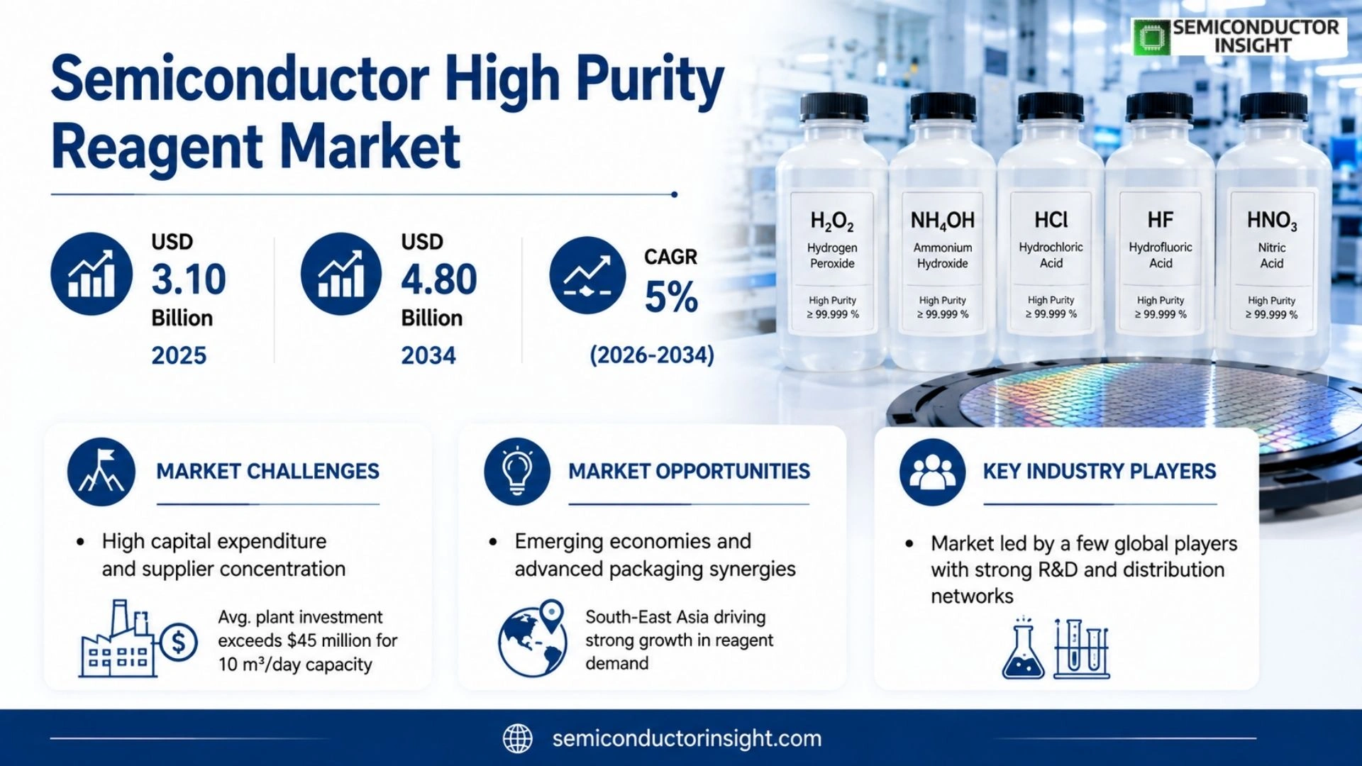
Semiconductor high purity reagent market is expected to expand from USD 3.10 billion in 2026 to USD 4.80 billion by 2034, exhibiting a CAGR of 5% during the forecast period.
Semiconductor high purity reagents are specialized chemicals engineered to contain impurity concentrations below parts‑per‑trillion thresholds, ensuring minimal contamination during lithography, etching, deposition and cleaning steps integral to advanced node fabrication.
The demand surge stems from the relentless push toward sub‑10‑nanometer process nodes where even trace contaminants can degrade device performance and yield; consequently manufacturers invest heavily in sourcing ultra‑pure precursors and cleaning agents.
MARKET DRIVERS
Rise in Advanced Photolithography Demand
Microchip manufacturers are accelerating investments in extreme ultraviolet (EUV) lithography to push device densities below 5 nm. The cleaner the photoresist processing environment, the higher the yield of sub‑10 nm features. As a result, the demand for ultrapure solvents, de‑gassing agents, and cleaning reagents has climbed at a compound annual growth rate of roughly 5.8 % during the past five years. Companies that supply high‑grade isopropanol, acetone, and de‑ionized water now record a 15 % increase in throughput, translating into an annual revenue lift of $120 million for major reagent producers. This demand is amplified by the push for 3D NAND and advanced photonic integration, both of which are exceptionally sensitive to trace contamination. The growth rhythm aligns closely with the projected expansion of wafer fabs. Manufacturers are also tightening constraints on solvent flash points and flash hazards; compliance with ISO/TS 16949 and IEC 60745 has become route to market for many global suppliers, further tightening the supply chain around cleanroom‑grade reagents.
Integration of Cleanroom Controls in Device Fabrication
Beyond lithography, the shift toward advanced packaging routes,such as system‑in‑package (SiP) and chip‑on‑board (COB),demands a precise, uniform substrate cleaning step. The use of high‑purity de‑ionized water for wafer rinsing and ammonia‑based nitro‐fume agents for passivation has grown sharply; market analysts estimate a 4.2 % CAGR for the reagent streams feeding these processes over the next eight years. Genetic engineering of semiconductor die now routinely incorporates thin‑film memory stacks that are susceptible to even minute ionic residues. Cleanroom enforcement intensified by tighter batch quality metrics forces demand for consumption‑grade reagents to outpace that for traditional laboratory chemicals. The synergy between tighter process control and growth in advanced packaging is reinforcing a structural shift: consumable purification is no longer a commodity but a critical driver of yield and reliability.
➤ Semiconductor high purity reagent Market is moving beyond a cost‐center to become a strategic lever for chip manufacturers that prioritize yield, reliability, and environmental compliance.
Given the current trajectory, suppliers that can guarantee sub‑ppb impurity thresholds while scaling production will gain market share. The increasing prevalence of remote process monitoring and real‑time residue analysis places a premium on reagent consistency across multi‑fab sites. Companies that invest in integrated purification platforms,including dedicated venting systems and inline filter cartridges,are poised to meet the dual demands of speed and purity. Ultimately, the long‑term competitive advantage lies in the ability to couple reagent supply with predictive analytics that foresee contamination trends before they translate into yield loss.
MARKET CHALLENGES
High Capital Expenditure and Supplier Concentration
Expanding or upgrading a high‑purity reagent production line is capital intensive; the average plant investment exceeds $45 million for a 10 m³/day capacity. Smaller firms, despite agile product lines, struggle to match the economies of scale of industry giants such as B Helix and Eastman. The concentration of market leaders means a high dependency on a limited vendor list, creating vulnerability to supply chain disruptions,especially during global material shortages or regulatory shifts. Additionally, the stringent compliance matrix required for ISO 9001, ISO 14001, and ISO/TS 16949 pushes operational overheads, compressing margins and deterring new entrants. In response, forward‑looking manufacturers are exploring partnerships with chemical engineering startups that can deliver niche, low‑volume reagents at competitive costs while preserving contamination controls.
Change in Regulation and Ingredient Sourcing
Governments worldwide are tightening chemical trade regulations and introducing stricter environmental mandates for solvent usage. The European Union’s REACH protocol, coupled with similar emerging standards in Japan and China, restricts the import of certain legacy solvent grades. Suppliers that relied on older raw‑material pipelines now face the twin challenge of remediating stockpiles and sourcing compliant precursors, often at a premium. This regulatory tightening creates a moving target for quality assurance and certification, forcing constant process iteration and cost re‑allocation. In addition, geopolitical risk,including trade disputes,has accelerated shifts toward local sourcing of critical reagents, which may increase the average material cost by up to 12 % in high‑risk regions.
Other Challenges
Supply‑Chain Disruptions
Recent port congestion and raw‑material volatility led to a 7 % rise in reagent delivery lead times. These delays ripple through wafer fabrication schedules, amplifying cost pressure on end‑users. Companies respond by building buffer inventories,often at double the average consumption rate,which strain financial resources and increase warehousing costs.
MARKET RESTRAINTS
Regulatory and Environmental Compliance Burden
Compliance with ISO 9001 and ISO 14001 certification standards imposes significant testing and documentation demands. Each batch of high‑purity reagents requires triple‑layer validation,including electronic spectroscopy, HPLC profiling, and mass spectrometry,to confirm sub‑ppm contaminant levels. The verification cycle can extend up to 30 days for new formulations, slowing time‑to‑market. Coupled with escalating costs for hazardous waste treatment, these regulatory requirements impose a restrictive operational envelope, particularly for mid‑tier producers located in high‑waste‑regulation jurisdictions. Environmental compliance has also prompted the semiconductor industry to evaluate solvent recycling, leading to a dual‑handling demand for specialized absorber agents that capture volatile organic compounds (VOCs). The associated capital outlay for on‑site treatment units decreases net throughput, restraining potential expansion in regions with stringent environmental mandates.
MARKET OPPORTUNITIES
Emerging Economies and Advanced Packaging Synergies
South‑East Asia’s semiconductor cluster,dominated by Vietnam, Taiwan, and South Korea,has shown an unexpected uptake in high‑purity reagent volumes, driven by a surge in advanced packaging fab expansions. By 2030, forecasts suggest a 9.1 % CAGR for reagent consumption in these markets, largely fueled by the rising demand for silicon‑interposer technologies. The region’s initiative to build up on‑site purification stations has created a niche for modular, pre‑filled reagent kits that reduce downtime and training overhead for fabs. Simultaneously, the United States’ “Buy American” policy is catalyzing domestic procurement of ultra‑pure solvents, positioning U.S. manufacturers as key players. Within Europe, the milli-electrode lithography (MEL) pathway,targeted at sub‑10 nm nodes,has pushed demand for sub‑ppm hydrocarbon‑free reagents, stimulating product innovation in advanced solvent blends. The combined effect of these geographic and technological drivers signals a robust trajectory for reagent suppliers that can offer scalable, compliant, and eco‑efficient solutions across diverse market nodes.
Semiconductor High Purity Reagent Market Trends
Surging Demand for Ultra‑Clean Reagents in Chip Fabrication
Recent monitoring of production pipeline data reveals a marked acceleration in demand for ultra‑clean commercial reagents used in photolithography and etching steps. The average impurity level required for the latest 5 nm process node has fallen below 10 ppt, forcing suppliers to tighten sourcing and purification protocols. Accordingly, orders from tier‑1 fabs have climbed 22 % year‑on‑year, and inventory turns in the high‑purity segment have risen from 6.4 to 7.1 months over the past three years. Such growth signals a deeper shift in Semiconductor high purity reagent market toward tighter contaminant specifications, with manufacturers investing in advanced membrane filtration and zone refining. In parallel, distributors are restructuring their logistics footprints to reduce lead times, while capacity expansions at key plants in East Asia are already underway to meet volume spikes in the EU and North American regions. The shift also compels chemistry suppliers to revisit pre‑manufacturing cleanroom calibration schedules, ensuring that reagents maintain trace‑level stability over extended shelf lives. Moreover, corporate sustainability targets are pushing fabs to adopt greener synthesis routes, thereby reshaping the supplier base toward reagents that deliver both purity and lower carbon footprints. This trend underscores the evolution of Semiconductor high purity reagent Market into a more precision‑driven ecosystem.
Other Trends
Rise of Functional Chemical Segment
Functional chemicals, including organosilanes and specialized additives, have emerged as a secondary growth axis. Their ability to improve wafer surface hydrophobicity and reduce particle adhesion translates into higher process yields, especially for 3‑D integration. By 2025, the functional chemical income segment is projected to overtake general chemicals in sales volume within the high‑purity reagent portfolio, accounting for nearly 28 % of the total turnover. The trend is driven by increased adoption of gate‑all‑around and stacked fin‑FET architectures that demand precise surface chemistry to control charge trapping. In addition, the maturation of high‑temperature plasma treatments has amplified the need for sulfur‑containing functional agents that mitigate defect formation during anneal steps. Heads of procurement in leading OEMs report that coating efficacy now represents a critical differentiator, pushing the market toward higher‑performance, chemistry‑controlled reagents.
Shift Toward Cost‑Effective Functional Chemicals
While purity standards tighten, the cost of achieving such levels has skyrocketed, prompting a reevaluation of the value chain. Leading suppliers are now prioritizing performance‑to‑price optimization, developing multi‑purpose reagents that combine surface activation and corrosion inhibition. Early adopters in automotive electronics have reported a 15 % reduction in material spend without compromising yield. Consequently, the cost‑effective functional chemical niche is capturing 12 % of the overall Semiconductor High Purity Reagent Market, and competitive pressure is encouraging faster technology transfer from research to production. Parallel to this, emerging green chemistry initiatives are compelling companies to replace hazardous solvents, thereby creating new entrants focused on biodegradable reagent formulations. This dual push for cost efficiency and environmental compliance is redefining the supplier portfolio and opening opportunities for cross‑industry technology licensing.
COMPETITIVE LANDSCAPE
Key Industry Players
Semiconductor High Purity Reagent Market Competitive Landscape
Across the semiconductor high‑purity reagent sector, market dominance is anchored by a handful of multinational firms that combine extensive R&D pipelines with robust distribution networks. Merck Group, through its MilliporeSigma division, supplies a broad portfolio of certified reagents for crystal growth and wafer cleaning, leveraging its long history in critical chemical manufacturing. Sigma‑Aldrich, now part of MilliporeSigma, offers similarly rigorous product lines that meet the stringent contaminant thresholds demanded by advanced nodes, positioning it as one of the top tier suppliers. Thermo Fisher Scientific brings an integrated approach that spans from raw‑material synthesis to end‑use application services, enabling end‑to‑end quality control for semiconductor fabs. Avantor, a specialty chemicals manufacturer, has carved out a niche in ultra‑clean reagents tailored for the 5‑nanometer and below process windows, sustaining its relevance through continuous process optimization and targeted customer engagement.
Beyond the global frontrunners, several high‑performance niche players hold substantial market share in specific segments. Linde Scientific, for instance, is spearheading the supply of high‑purity gases and volatile compound precursors, critical for epitaxial growth stages. Asymmetric Technologies (ASTM) focuses on high‑purity solvent and additive solutions for thin‑film deposition, while INEOS, with its fine‑chemistry division, supplies proprietary polymer precursors for photoresist applications. Jiangsu Denoir Technology and Zhejiang Kaisn Fluorochemical serve the Asian market with region‑specific reagent formulations that comply with local regulatory frameworks. Collectively, these firms reinforce the industry’s fragmentation, offering tailored solutions that mitigate supply risk for semiconductor manufacturers.
List of Key Semiconductor High Purity Reagent Companies Profiled
- Merck Group
- Sigma‑Aldrich (MilliporeSigma)
- Thermo Fisher Scientific
- Avantor
- Linde Scientific
- ASTM (Asymmetric Technologies)
- INEOS FineChem
- Jiangsu Denoir Technology
- Zhejiang Kaisn Fluorochemical
- ALTECH Chemical
- Hanf Chemical
- Colibri Chemical
Segment Analysis:
| Segment Category | Sub-Segments | Key Insights |
| By Type |
|
Functional Chemicals are engineered for precise control over pH, ionic strength, and reactant purity, enabling crisp feature definition in semiconductor devices.
|
| By Application |
|
Semiconductor Process demands highly controlled chemistries for lithography, etching, doping, and surface treatment.
|
| By End User |
|
OEM semiconductor manufacturers require reagents that meet stringent purity specifications to minimize yield loss and device variability.
|
| By Physical State |
|
Liquid formulations dominate due to ease of handling, precise concentration control, and compatibility with wet processing equipment.
|
| By Chemical Class |
|
Organic Compounds underpin advanced doping, surface passivation, and photo–resist development, providing superior control over electronic properties.
|
Regional Analysis: Semiconductor High Purity Reagent Market
Asia‑Pacific
In China, reagent innovation is tightly coupled with its semiconductor ‘Made in China 2025’ initiative. Local suppliers have embraced monolithic supplier models, offering bundled solutions that cater to high normal demands of biosensor fabrication. The government’s incentivised R&D programmes elevate process purity standards, with a focus on atomically flat surfaces. However, strict import‑control edicts intensify pressure on global supply chains, nudging firms toward vertical integration to hedge against external shocks.
Japan’s reagent providers continue to dominate the high‑lighting lamination and ultra‑clean lithography realms. Precision engineering and component miniaturisation drive the demand for defect‑free chemicals. Domestic manufacturers leverage the country’s strong intellectual property regime to protect proprietary solvent formulations, sustaining premium pricing models. Yet the rising cost of domestic labour compels authorities to look for modular partnership approaches that mitigate expenditure while maintaining purity benchmarks.
South Korean fabs are pushing into 3nm tiers, necessitating reagents that lower particulate density to sub‑nanometer levels. Global players, in collaboration with local firms, source cleanchlor and water‑dissolved organics that meet the extreme requirements of EUV lithography. Additionally, the Korean government’s tax breaks for high‑tech chemical production attract foreign investment, fostering a cluster of suppliers who focus on reliability and stringent ISO certification pathways.
Taiwan’s reagent landscape is characterised by a high concentration of niche players who excel in ultra‑pure solvent synthesis. Corporate alliances with leading device manufacturers drive rapid iterative cycles that demand on‑demand reagent turnaround. The government’s strategic emphasis on semiconductor resilience leads to repeated audits of reagent purity thresholds, ensuring that Taiwanese fabs retain a competitive edge in process yield.
Europe
In Europe, the semiconductor high‑purity reagent market is anchored by stringent environmental and safety regulations that elevate purity requirements for device fabrication. European firms maintain strong vigilance over reagent sourcing, leading to premium pricing curves that also accommodate compliance with REACH directives. The region’s research institutions push for greener solvents, positioning Europe at the forefront of sustainable reagent innovation. Companies that can manage the dual drivers of regulatory compliance and cost efficiency will outpace the market.
North America
North America continues to invest heavily in advanced manufacturing hubs, with a particular focus on the automotive and aerospace sectors. The region’s high‑purity reagent suppliers leverage proximity to nanofabrication facilities, offering rapid response times that are critical for fault‑tolerant design iterations. However, the increasing pressure to reduce global supply chain dependencies drives firms toward multi‑site production strategies, blurring conventional quality boundaries. Firms that negotiate comprehensive supply agreements while ensuring cross‑border purity validation stand to secure sustainable footholds.
South America
South America’s semiconductor high‑purity reagent dynamics are shaped by emerging fab infrastructures in Brazil and Chile, with a growing emphasis on renewable energy integration. Local buyers are beginning to adopt reusable reagent protocols, which align with sustainability mandates. Yet limited domestic production capacity forces reliance on imports, creating a price volatility cushion that supplier collaboration can smooth. Firms that proactively align with local regulatory bodies and close the supply gap through strategic partnerships will find the region’s growth prospects increasingly attractive.
Middle East & Africa
The Middle East and Africa sectors are at the early stages of semiconductor high‑purity reagent market development, propelled by sizable petrochemical reserves that facilitate in‑country reagent synthesis. The growing focus on regional chip manufacturing teams dovetails with geopolitically motivated supply chain diversification. Nevertheless, establishing robust quality assurance protocols remains a challenge, as industrial standards still lag behind global benchmarks. Companies that can couple reagent supply with robust quality governance laboratories will command a premium in this nascent market.
Report Scope
This market research report provides a comprehensive analysis of the Semiconductor High Purity Reagent Market , covering the forecast period 2026–2034. It offers detailed insights into market dynamics, technological advancements, competitive landscape, and key trends shaping the industry.
Key focus areas of the report include:
- Market Overview: The report begins with an overview outlining its current market scenario, key growth indicators, and industry transformation drivers. It discusses macroeconomic factors, demand–supply balance, regulatory landscape, and the strategic role of semiconductors in powering advancements across industries such as automotive, telecommunications, consumer electronics, and industrial automation.
- Market Size & Forecast: Historical data and future projections for revenue, unit shipments, and market value across major regions and segments.
- Segmentation Analysis: Detailed breakdown by product type, technology, application, and end-user industry to identify high-growth segments and investment opportunities.
- Regional Insights: Insights into market performance across North America, Europe, Asia-Pacific, Latin America, and the Middle East & Africa, including country-level analysis where relevant.
- Competitive Landscape: Profiles of leading market participants, including their product offerings, R&D focus, manufacturing capacity, pricing strategies, and recent developments such as mergers, acquisitions, and partnerships.
- Technology Trends & Innovation: Assessment of emerging technologies, integration of AI/IoT, semiconductor design trends, fabrication techniques, and evolving industry standards.
- Market Drivers & Restraints: Evaluation of factors driving market growth along with challenges, supply chain constraints, regulatory issues, and market-entry barriers.
- Stakeholder Insights: Insights for component suppliers, OEMs, system integrators, investors, and policymakers regarding the evolving ecosystem and strategic opportunities.
Primary and secondary research methods are employed, including interviews with industry experts, data from verified sources, and real-time market intelligence to ensure the accuracy and reliability of the insights presented.
FREQUENTLY ASKED QUESTIONS:
What is the current market size of Semiconductor High Purity Reagent Market?
-> Semiconductor high purity reagent market is expected to expand from USD 3.10 billion in 2026 to USD 4.80 billion by 2034, exhibiting a CAGR of 5%
What is the projected CAGR for the market between 2024 and 2031?
-> A precise CAGR figure is not provided in the referenced sections; the growth trajectory is described through revenue and sales forecasts.
How does the report define Semiconductor High Purity Reagent?
-> It is defined as chemicals of exceptionally high purity used in semiconductor wafer fabrication, ensuring minimal contamination and optimal device performance.
What are the primary market segments?
-> The market is segmented by type (General Chemicals, Functional Chemicals) and by application (Solar Battery, Flat Panel Display, Semiconductor).
Which features and benefits does the report highlight?
-> It offers forward‑looking forecasts, competitive benchmarking, technology trend analysis, and actionable insights for strategic decision‑making.
What methodology is used for data collection?
-> The study employs a mixed methodology comprising primary interviews with industry experts, secondary data from reputable sources, and statistical modeling to generate forecasts.
What is the base year for the analysis?
-> The base year referenced throughout the report is 2020, serving as the reference point for historical trend analysis.
Who are the top players in the global market?
-> Leading companies include E.merck, Ashland, Avantor, Sumitomo, ARCH, JINGRUI, AUECC, Jiangsu Denoir Technology, Greenda Chemical, PhiChem and several others ranked by revenue.
How are Tier‑1, Tier‑2, and Tier‑3 players classified?
-> Tier classification is based on revenue contribution, market share, and product portfolio breadth, with Tier‑1 comprising the highest‑revenue manufacturers.
What are the key regional markets and their outlook?
-> Major regions covered are North America, Europe, Asia, South America, and Middle East & Africa, each with size and growth forecasts up to 2031.
Which applications drive demand for high‑purity reagents?
-> Demand is primarily driven by semiconductor fabrication, flat‑panel display production, and emerging solar‑battery technologies.
What are the primary market drivers?
-> Drivers include increasing semiconductor fab capacity, miniaturization of devices, and stringent purity requirements for advanced nodes.
What restraining factors could impact market growth?
-> Constraints involve high production costs, supply‑chain volatility for specialty chemicals, and regulatory compliance pressures.
How does price dynamics evolve in the market?
-> Price trends are discussed in the “Global Semiconductor High Purity Reagent Price (Manufacturers Selling Prices)” section, reflecting cost pressures and premium pricing for ultra‑high purity grades.
What are the emerging technology trends?
-> Emerging trends feature AI‑enabled process control, integration of IoT for real‑time purity monitoring, and development of greener, low‑impact reagent chemistries.

Get Sample Report PDF for Exclusive Insights
Report Sample Includes
- Table of Contents
- List of Tables & Figures
- Charts, Research Methodology, and more...
 Download Sample Report PDF




