SEMICONDUCTOR INSIGHT
MARKET RESEARCH REPORT

Semiconductor Photoresist Market

2026 to 2034
MARKET INTELLIGENCE
ACROSS KEY REGIONS
2026 EDITION
SEMICONDUCTOR EQUIPMENT Semiconductor Market Research

Semiconductor Photoresist Market

Emerging Trends, Technological Advancements, and Business Strategies 2026-2034

◷
UPDATED 15 September 2026
▤
REPORT LENGTH Detailed Report
▣
REPORT CODE 37b4bc09cee9
▯
FORMATS PDF

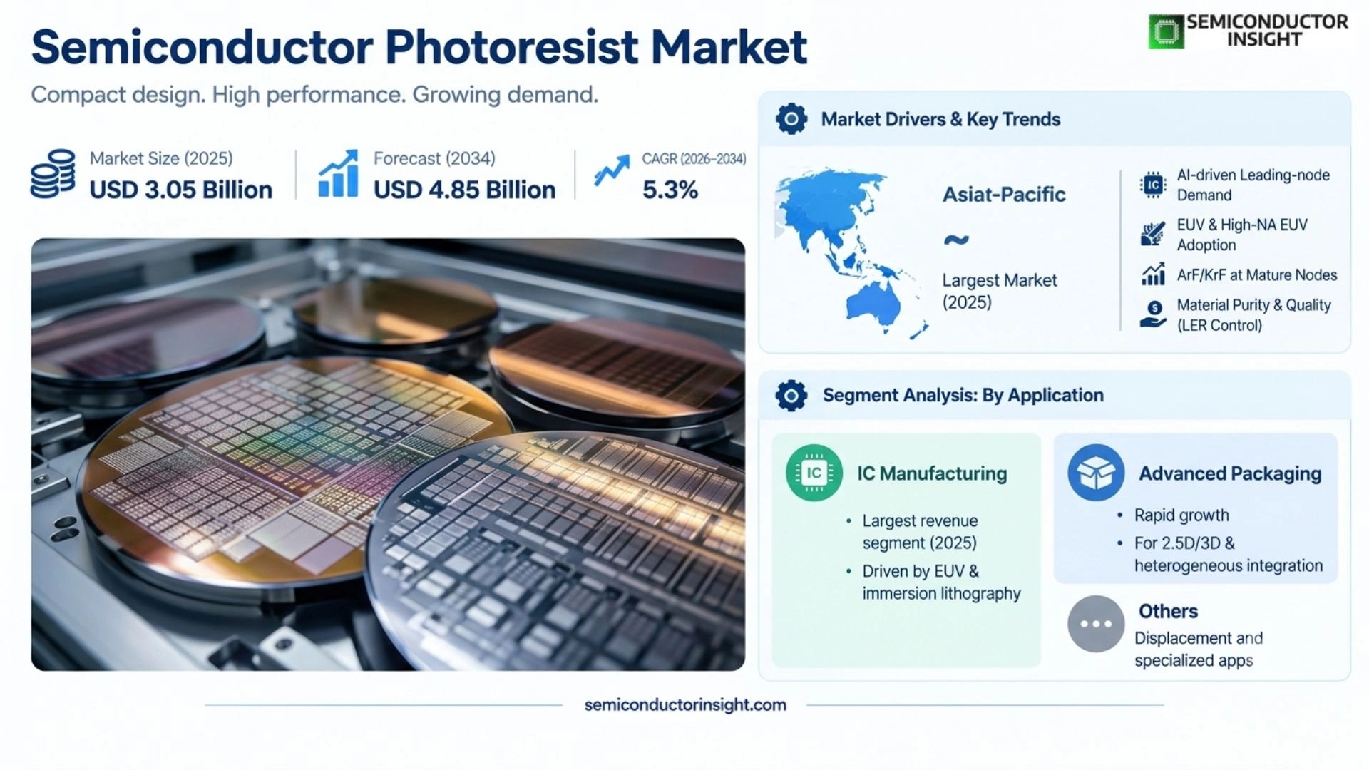
Semiconductor Photoresist Market is rebased to USD 3.05 billion in 2025, increases to an estimated USD 3.21 billion in 2026, and is projected to reach USD 4.85 billion by 2034. The selected source-page size anchors imply a 5.3% CAGR during 2026–2034. Asia Pacific is the largest market in 2025, while current demand is being reshaped by AI-driven leading-node wafer starts, EUV and High-NA EUV adoption, continued ArF/KrF demand at mature nodes, local semiconductor-material capacity expansion and stricter requirements for purity, line-edge roughness and stochastic-defect control.

Get the sample PDF with study scope, segmentation and methodology details.

Key Statistics

2025 Market Size
USD 3.05 billion
2034 Projected Market Size
USD 4.85 billion
CAGR (2026–2034)
5.3%
Largest Market in 2025
Asia Pacific

Key Takeaways

  • EUV Photoresist is the fastest-growing type on the source page because leading logic and advanced memory increasingly depend on EUV patterning. Current 2026 supplier activity-TOK’s EUV partnership, JSR/Inpria cross-licensing and Sumitomo Chemical’s new photoresist technology center-confirms that EUV materials remain the main innovation battleground.
  • ArFi and KrF remain essential volume products. The source page states that DUV photoresists account for most market value because mainstream and mature nodes still use ArF immersion, KrF and g/i-line lithography extensively. The market therefore grows through a mix of leading-edge premium value and large mature-node wafer volume.
  • IC Manufacturing is the largest application because front-end wafer fabrication consumes photoresist repeatedly across many lithography layers. Advanced packaging creates a secondary growth stream through redistribution layers, bumping and thick-film patterning where resist thickness, adhesion and aspect-ratio performance differ from front-end requirements.
  • Asia Pacific leads the market because Taiwan, South Korea, Japan and China concentrate leading logic, memory and materials manufacturing. Supplier proximity matters because resist qualification requires frequent fab interaction, controlled logistics and rapid response to yield excursions.
  • The source page’s headline forecast is internally inconsistent. USD 3.05 billion in 2025 and USD 4.85 billion in 2034 imply approximately 5.3% CAGR, not the printed 7.1%; the anchor-derived 5.3% rate is therefore used throughout this article.

Semiconductor Photoresist Market Overview

Semiconductor Photoresist Market is rebased to USD 3.05 billion in 2025, increases to an estimated USD 3.21 billion in 2026, and is projected to reach USD 4.85 billion by 2034. The selected source-page size anchors imply a 5.3% CAGR during 2026–2034. Asia Pacific is the largest market in 2025, while current demand is being reshaped by AI-driven leading-node wafer starts, EUV and High-NA EUV adoption, continued ArF/KrF demand at mature nodes, local semiconductor-material capacity expansion and stricter requirements for purity, line-edge roughness and stochastic-defect control.

Base year: 2025 · Estimated year: 2026 · Forecast period: 2026–2034 · Values in USD million unless stated otherwise

Semiconductor photoresists are ultra-high-purity photosensitive materials applied to wafers before exposure so that circuit patterns can be transferred through lithography, development and subsequent etch or deposition steps. Product performance is defined by resolution, sensitivity, line-edge roughness, etch resistance, defectivity, outgassing, film uniformity and compatibility with track and exposure tools. Because lithography is repeated many times per wafer, a small material excursion can affect yield across a large amount of downstream process value.

The product mix spans g/i-line, KrF, ArF dry, ArF immersion and EUV formulations, and each technology remains economically relevant because semiconductor manufacturing contains many process generations simultaneously. Leading logic and advanced memory use EUV for critical layers, while ArF immersion remains deeply embedded in multi-patterning and mature advanced nodes. KrF and g/i-line continue to serve power, analog, MEMS, image-sensor, display-related and packaging applications where the process window and cost structure favor established optical wavelengths.

Current supplier investment shows that demand is not simply a function of semiconductor units. TOK acquired additional land in Koriyama in March 2026 near an existing photoresist and high-purity-chemical plant, Sumitomo Chemical announced a new Osaka technology center for EUV and ArF photoresists in April 2026, and Fujifilm is expanding advanced resist development around AI semiconductor requirements. These moves indicate that technical support, quality evaluation and local supply assurance are becoming as important as nominal formulation capacity.

Segment Analysis: By Type

The source page segments the market into EUV Photoresist, ArFi Photoresist, KrF Photoresist and g/i-Line. EUV is the fastest-growing technology because it enables the most advanced lithography steps, while ArFi, KrF and g/i-line maintain large installed-volume demand across mainstream, mature-node and packaging processes. The market is therefore technologically stratified rather than undergoing a simple one-way replacement of older resist generations.

Type Technical / commercial role Market position
EUV Photoresist EUV resists are exposed at 13.5 nm and must generate extremely small features while controlling stochastic defects, line-edge roughness, sensitivity and outgassing under a very small photon budget. Chemically amplified resists, metal-oxide resists and newer molecular platforms are all being developed because High-NA EUV places more severe demands on film thickness, pattern collapse and process latitude. Fastest-growing and highest-R&D segment. TOK announced a 2026 partnership with Irresistible Materials around Multi-Trigger Resist, while JSR/Inpria and Entegris cross-licensed metal-oxide-resist patents. Supplier differentiation therefore depends on platform technology, fab co-development and the ability to scale a laboratory formulation into ultra-clean high-volume manufacturing.
ArFi Photoresist ArF immersion uses 193 nm light with water between the final lens and wafer to increase numerical aperture and resolution. It remains critical for many advanced and mainstream process layers, including devices that also use EUV. Formulations must manage immersion compatibility, defects, topcoat behavior, leaching and dense/isolated pattern performance under high-volume scanner conditions. Large and durable value segment. Fujifilm’s 2026 development of a fluorine-free negative ArF immersion resist for advanced AI-semiconductor nodes shows that innovation continues even as EUV expands. Environmental requirements, cost reduction and pattern flexibility can therefore create new product opportunities inside a mature lithography platform.
KrF Photoresist KrF photoresists use 248 nm exposure and serve mature logic, memory, analog, power, MEMS and many specialty processes. KrF can provide strong throughput and cost performance where feature sizes do not require ArF or EUV. The manufacturing challenge is maintaining very high purity and consistency at substantial volume while responding to long product lifecycles and customer-specific process windows. High-volume mature segment with relatively stable demand. TOK states that it holds a leading share in KrF photoresists, reflecting the value of scale and customer qualification even in older technology. Growth is slower than EUV, but mature-node fab expansions in automotive, industrial and power electronics protect the installed demand base.
g/i-Line g-line and i-line resists use longer-wavelength mercury-lamp lithography and remain important in power semiconductors, MEMS, sensors, compound semiconductors, display-related processes and advanced packaging. Thick-film variants can support electroplating molds, bumps and redistribution layers where resist thickness and sidewall profile matter more than sub-20-nm resolution. Long-lived specialty segment. TOK highlights thick-film i-line products for power semiconductor applications, while packaging complexity creates additional demand for thick resists. This segment competes on application-specific adhesion, film thickness, thermal behavior and develop profile rather than on leading-edge transistor pitch.

Secondary segmentation: By Technology Node

The source page further segments demand into Advanced Nodes (<10nm), Mainstream Nodes (10–28nm) and Mature Nodes (>28nm). Node classification changes the required resist family, defect tolerance, process complexity and customer qualification burden, so market value does not scale directly with wafer volume. For photoresist suppliers, the commercial consequence is that fab qualification, purity, defectivity and process integration determine revenue quality much more directly than broad semiconductor shipment growth or nominal chemical production volume.

Technology node Photoresist demand mechanism
Advanced Nodes (<10nm) Leading logic and advanced memory consume EUV and ArF immersion photoresists with the tightest controls on purity, stochastic defects and line-edge roughness. Each wafer can use many critical lithography layers, and the processed wafer value is very high, so customers prioritize yield and stable supply over lowest material price. High-NA EUV development further raises R&D intensity.
Mainstream Nodes (10–28nm) These nodes use combinations of ArF immersion, ArF dry and KrF depending on layer requirements. High wafer volumes in mobile, networking, automotive and industrial products create significant resist consumption. Supplier competition balances technical differentiation with scale, because customers require mature high-yield formulations and dependable local delivery.
Mature Nodes (>28nm) Mature-node fabs use KrF and g/i-line heavily across power, analog, MEMS, sensors and embedded control devices. Product lifecycles can extend for many years, making change control and continuity important. Growth is slower than advanced logic, but new capacity for automotive and industrial semiconductors sustains a broad base of qualified formulations.

Secondary segmentation: By Imaging Mechanism

The source page also divides the market into Positive, Negative and Hybrid Photoresists. Positive resists are described as the dominant mechanism because exposed areas become more soluble and are widely used in semiconductor lithography, while negative and hybrid approaches can offer process advantages for specialty or next-generation patterning. This matters because photoresist is approved on specific lithography layers and tool conditions, so a formulation becomes commercially valuable only when it reproduces patterning performance and yield consistently in high-volume customer manufacturing.

Imaging mechanism Commercial relevance
Positive Photoresists Positive-tone systems dominate many semiconductor processes because they offer established process control and high-resolution capability. They are deeply integrated with DUV and EUV chemically amplified platforms. Suppliers compete on dissolution contrast, sensitivity, roughness and defectivity while maintaining compatibility with the fab’s track, developer and etch sequence.
Negative Photoresists Negative-tone systems retain exposed material and can provide advantages for specific pattern shapes, thick films and advanced process flows. Fujifilm’s 2026 fluorine-free negative ArF immersion development demonstrates that negative tone can also be relevant to advanced nodes when it lowers environmental impact or improves formation of selected geometries.
Hybrid Photoresists Hybrid or alternative platforms combine chemical or inorganic approaches to improve the resolution-sensitivity-roughness trade-off. Metal-oxide resists and molecular resists are important examples for EUV. Commercial success depends on demonstrating full integration into track, exposure, etch and defect-control flows rather than only achieving strong isolated lithography metrics.

Secondary segmentation: By End User

The source page identifies Foundries, IDMs and OSATs as end users. Foundries are the primary front-end consumers because they run high-volume logic and specialty fabs, IDMs use resists across memory, logic, analog and power processes, and OSATs consume specialized thick-film and packaging resists for redistribution and interconnect formation. The purchasing decision therefore combines lithographic performance, contamination control, local technical support, batch consistency and supply assurance rather than treating the material as an interchangeable specialty chemical.

End user Demand characteristics
Foundries Foundries qualify multiple photoresist families across many process nodes and customer designs. Their large wafer starts make supply assurance critical, while advanced nodes require intensive co-development with material suppliers. A formulation that wins a process-layer qualification can generate recurring volume over several years, but any defect excursion can threaten many fabless customer products simultaneously.
IDMs Integrated device manufacturers use photoresists in memory, processors, analog, power and specialty devices. They can maintain proprietary process recipes for long periods and often co-develop materials directly with suppliers. Memory IDMs are especially important to EUV and ArF demand because high-layer-count devices use repeated lithography steps at large wafer volumes.
OSATs OSATs use photoresists mainly in wafer-level packaging, redistribution, bumping and related processes rather than transistor formation. These applications often require thicker films, high aspect ratio and strong adhesion. Advanced packaging therefore creates an adjacent growth pool with a different formulation and equipment set from front-end EUV lithography.

Segment Analysis: By Application

By application, the source page segments demand into IC Manufacturing, Advanced Packaging and Others. IC Manufacturing dominates because front-end fabrication requires repeated lithography across many wafer layers, while advanced packaging is gaining importance as chiplets, redistribution layers, bumping and heterogeneous integration increase the number and complexity of back-end patterning steps.

Application Demand characteristics
IC Manufacturing Front-end IC fabrication is the largest application because photoresist is coated, exposed and developed repeatedly during logic, memory, analog and power-device production. Advanced nodes use premium EUV and ArF formulations, while mature nodes consume large volumes of KrF and g/i-line. Total demand is therefore driven by both wafer starts and the number of lithography layers per wafer.
Advanced Packaging Wafer-level packaging, fan-out, redistribution layers, micro-bumps and interposers use specialized photoresists with thicker films, high aspect ratio, plating resistance and strong adhesion. Growth in chiplets and heterogeneous integration expands this application even when front-end wafer starts are unchanged because more patterning occurs after the transistor fabrication process.
Others Other applications include MEMS, compound semiconductors, photonics, magnetic heads, sensors and specialty microfabrication. These processes can use i-line, KrF, e-beam or customized formulations with unusual substrate, thickness or thermal requirements. Volumes are smaller but switching costs can be high when a resist becomes embedded in a long-qualified specialty process.

Semiconductor Photoresist Market Size

Regional Analysis

Asia Pacific is the largest market because Taiwan, South Korea, Japan and China concentrate leading logic, advanced memory, mature-node fabs and the major Japanese photoresist supplier base. The source page explicitly identifies Asia-Pacific as dominant and emphasizes local supply integration, while North America is expanding materials and fab capacity through localization programs.

Why does semiconductor photoresist demand remain geographically concentrated?

Photoresist is a high-purity, process-specific consumable whose performance must be tuned to individual scanners, tracks and fab recipes. Customers therefore value local manufacturing, technical centers and rapid troubleshooting near semiconductor clusters. Asia Pacific combines the largest wafer-start base with major suppliers, North America is adding leading-edge fabs and local materials support, Europe specializes in automotive and industrial semiconductors, and other regions remain smaller.

Region Position Growth outlook Demand profile What decides supplier selection
Asia Pacific Largest High Leading logic, memory and materials-led Local technical support, purity, qualification and supply continuity
North America Strategic expansion High Leading-edge logic, AI and specialty fabs Localization, advanced-node capability and customer co-development
Europe Specialty strength Moderate to high Automotive, power, MEMS and industrial-led Environmental compliance, specialty formulations and reliability
South America Niche Low to moderate Automotive and specialty semiconductor-led Imports, distributor support and mature-node availability
Middle East & Africa Emerging Low from small base Planned semiconductor initiatives-led Technology transfer, partnerships and imported supply
Asia Pacific LARGEST

Why does Asia Pacific dominate photoresist demand?

Asia Pacific combines the largest concentration of semiconductor wafer fabs with the world’s leading photoresist manufacturing base. Taiwan and South Korea lead advanced logic and memory adoption, Japan hosts TOK, JSR, Shin-Etsu, Fujifilm and Sumitomo Chemical, and China is expanding both fab capacity and domestic materials capability. Through 2034, suppliers that combine next-generation EUV innovation with dependable ArF, KrF and i-line production can capture growth across both advanced and mature semiconductor nodes instead of relying on one technology transition.

Market positionLargest
Growth outlookHigh
Demand profileLogic, memory and materials-led
Market access gateFab qualification and local technical support
Country / subregion Position Demand mechanism
Japan Global materials technology center Japan hosts many leading photoresist suppliers and continues investing in EUV, ArF and high-purity chemical infrastructure. TOK purchased additional plant land in Koriyama in 2026, while Sumitomo Chemical announced a new advanced-photoresist technology center at Osaka Works.
Taiwan Leading-edge foundry demand Taiwan’s foundry ecosystem consumes EUV, ArF immersion, KrF and specialty resists across a very broad node range. Suppliers maintain local manufacturing or technical support because yield excursions require immediate collaboration and because high-volume wafer fabs need tightly controlled just-in-time material supply.
South Korea & China Memory and localization growth South Korea’s advanced memory fabs create high-volume EUV and DUV demand, while China’s expanding mature and advanced semiconductor capacity increases local consumption. Domestic Chinese suppliers are improving, but the most demanding processes still require long customer qualification and strong purity control.

Market instances

  • TOK announced in February 2026 a strategic investment and joint-development partnership with Irresistible Materials to accelerate EUV photoresist innovation. TOK plans to combine the partner’s Multi-Trigger Resist platform with its own high-volume manufacturing and quality-control capabilities, demonstrating how Japanese suppliers are broadening their technology portfolios for low-NA and High-NA EUV.
  • Sumitomo Chemical decided in April 2026 to construct a new photoresist technology center at Osaka Works that integrates manufacturing-process technology management, quality evaluation and analytical functions for EUV and ArF photoresists. The facility is intended to strengthen the supply system for advanced semiconductor materials, not merely increase generic chemical capacity.
  • Fujifilm stated in 2026 that it is focusing on advanced photoresists for AI semiconductors and aims to expand its share, while also showcasing EUV and PFAS-free resist research. This confirms that regional competition is shifting toward next-generation formulation performance and environmental compatibility as much as production volume. For photoresist manufacturers, the development matters because it changes a verifiable lithography platform, material qualification, production capability or supply condition and therefore has a direct connection to future fab adoption rather than representing a generic semiconductor trend.

Asia-Pacific leadership is reinforced by co-location. Photoresist suppliers can develop, manufacture and troubleshoot materials close to customers whose yield sensitivity is extremely high. That proximity shortens qualification cycles and makes it difficult for distant new entrants to compete purely on price. The market implication is that announced material availability has limited value until the exact formulation and production site pass customer qualification, making application engineering and analytical capability part of effective commercial capacity.

North America ADVANCED-NODE LOCALIZATION

What is driving photoresist demand growth in North America?

North America is expanding leading-edge logic, memory and specialty semiconductor manufacturing while also trying to localize critical materials. The region remains dependent on Japanese expertise but is becoming more important for supplier technical support, advanced EUV collaboration and packaging-oriented photoresists as new fabs ramp. For photoresist suppliers, the commercial consequence is that fab qualification, purity, defectivity and process integration determine revenue quality much more directly than broad semiconductor shipment growth or nominal chemical production volume.

Market positionStrategic expansion
Growth outlookHigh
Demand profileAI and leading-edge fab-led
Market access gateLocalization and advanced-node qualification
Country / subregion Position Demand mechanism
United States Primary expansion market New advanced fabs and AI-related semiconductor production increase demand for EUV and ArF materials. Suppliers need domestic or nearby technical support and resilient logistics because advanced photoresist is a high-purity production consumable with limited tolerance for shipment or formulation variability.
Canada Research and specialty role Canada contributes semiconductor research, photonics and specialty manufacturing rather than very large logic wafer starts. Demand is therefore more concentrated in R&D and specialty resist applications, with materials typically supplied through multinational North American channels.
Mexico Downstream electronics link Mexico’s strength is electronics and assembly rather than advanced wafer fabrication, so direct photoresist consumption remains limited. Future growth depends on whether North American semiconductor localization extends into additional front-end or packaging process capacity.

Market instances

  • JSR/Inpria and Entegris announced a May 2026 cross-licensing agreement around metal-oxide-resist intellectual property for EUV lithography. The agreement is relevant to North America because Inpria is a U.S.-based MOR technology platform and illustrates how advanced resist competition increasingly involves patent ecosystems and collaborative development rather than simple formulation sales. For photoresist manufacturers, the development matters because it changes a verifiable lithography platform, material qualification, production capability or supply condition and therefore has a direct connection to future fab adoption rather than representing a generic semiconductor trend.
  • TOK participates in the US-JOINT advanced-packaging consortium in California, where its high-purity photoresists and microfabrication technologies support next-generation package patterning. Although packaging resists differ from leading-edge front-end EUV products, the investment expands TOK’s U.S. technical engagement and customer access. For photoresist manufacturers, the development matters because it changes a verifiable lithography platform, material qualification, production capability or supply condition and therefore has a direct connection to future fab adoption rather than representing a generic semiconductor trend.
  • Fujifilm’s SPIE 2026 lithography program in San Jose presented EUV, nanoimprint and PFAS-free resist research. International conferences near U.S. chip-design and equipment customers remain commercially important because photoresist adoption begins through process-development collaboration long before high-volume material shipments. For photoresist manufacturers, the development matters because it changes a verifiable lithography platform, material qualification, production capability or supply condition and therefore has a direct connection to future fab adoption rather than representing a generic semiconductor trend.

North America is becoming more important as a development and localization market. Suppliers that place application engineering, IP collaboration and reliable material logistics near U.S. fabs can reduce customer risk even if bulk manufacturing remains partly in Japan or other Asian locations. This matters because photoresist is approved on specific lithography layers and tool conditions, so a formulation becomes commercially valuable only when it reproduces patterning performance and yield consistently in high-volume customer manufacturing.

Europe SPECIALTY & ENVIRONMENTAL FOCUS

What differentiates European photoresist demand?

Europe has less leading-edge logic volume than Asia or the United States but strong automotive, industrial, power, MEMS and specialty semiconductor manufacturing. Environmental policy and chemical regulation also increase attention to fluorinated substances, solvent handling and safer formulations, creating opportunities for differentiated DUV and specialty products. The purchasing decision therefore combines lithographic performance, contamination control, local technical support, batch consistency and supply assurance rather than treating the material as an interchangeable specialty chemical.

Market positionSpecialty strength
Growth outlookModerate to high
Demand profileAutomotive, power and MEMS-led
Market access gateRegulatory compliance and specialty performance
Country / subregion Position Demand mechanism
Germany Automotive and power semiconductor base German fabs and research institutes consume KrF, i-line, ArF and specialty resists for automotive, industrial and power applications. Long product lifecycles reward stable formulations and detailed change control more than rapid switching to every new lithography platform.
France R&D and specialty semiconductor demand France combines microelectronics research, image sensors, power and specialty semiconductor production. Photoresist suppliers can participate through application-specific materials, advanced packaging and public-private R&D programs rather than the very large EUV volumes seen in Asian leading-edge fabs.
United Kingdom & Benelux Research and equipment ecosystem The region contributes lithography research, equipment and materials innovation. Irresistible Materials, based in the UK, entered a 2026 EUV partnership with TOK, showing that European materials innovation can be commercialized through larger global manufacturing networks.

Market instances

  • TOK’s 2026 investment in UK-based Irresistible Materials links European resist R&D with Japanese high-volume manufacturing. The partnership is intended to commercialize a molecular Multi-Trigger Resist platform for EUV, demonstrating a model in which specialized European innovation enters global fabs through an established materials supplier. For photoresist manufacturers, the development matters because it changes a verifiable lithography platform, material qualification, production capability or supply condition and therefore has a direct connection to future fab adoption rather than representing a generic semiconductor trend.
  • Fujifilm developed a fluorine-free negative ArF immersion resist in April 2026 for advanced AI semiconductor nodes. Although the product is global, the reduction of fluorinated chemistry is especially relevant to European customers facing tighter environmental scrutiny and long-term pressure to reduce PFAS dependence. For photoresist manufacturers, the development matters because it changes a verifiable lithography platform, material qualification, production capability or supply condition and therefore has a direct connection to future fab adoption rather than representing a generic semiconductor trend.
  • European specialty fabs use lithography generations for many years because automotive and industrial products have long qualification lives. That creates a durable market for KrF, i-line and ArF materials even when EUV captures the innovation spotlight, giving suppliers opportunities in stable high-reliability formulations. For photoresist manufacturers, the development matters because it changes a verifiable lithography platform, material qualification, production capability or supply condition and therefore has a direct connection to future fab adoption rather than representing a generic semiconductor trend.

Europe’s value proposition is technical specialization and regulatory fit rather than maximum wafer volume. Suppliers that combine mature-node reliability with lower-impact chemistry and advanced packaging capability can build durable positions. Through 2034, suppliers that combine next-generation EUV innovation with dependable ArF, KrF and i-line production can capture growth across both advanced and mature semiconductor nodes instead of relying on one technology transition.

South America NICHE IMPORT MARKET

Where does South American photoresist demand come from?

South America remains a small direct photoresist market because front-end semiconductor fabrication is limited. Demand comes mainly from research, specialty electronics and limited regional semiconductor initiatives, with Brazil representing the largest potential base. Most advanced photoresists are imported through global chemical and semiconductor supply channels. The market implication is that announced material availability has limited value until the exact formulation and production site pass customer qualification, making application engineering and analytical capability part of effective commercial capacity.

Market positionNiche
Growth outlookLow to moderate
Demand profileSpecialty and research-led
Market access gateImports and distributor support
Country / subregion Position Demand mechanism
Brazil Largest regional opportunity Brazil has the region’s largest electronics and technology base, but limited high-volume semiconductor wafer fabrication. Direct resist consumption is concentrated in research, specialty processes and smaller semiconductor initiatives rather than mass leading-edge manufacturing.
Argentina Research-oriented demand University, laboratory and specialty technology programs create small-volume demand for photoresists and microfabrication chemicals. Flexibility, technical documentation and small-lot supply matter more than local high-volume manufacturing.
Rest of Region Early-stage demand Most countries import finished semiconductors, so direct photoresist demand is minimal. Material suppliers generally serve the region through distributors rather than dedicated local manufacturing.

Market instances

  • The source page describes South America as a niche photoresist market serving automotive and industrial semiconductor needs, with Brazil leading regional initiatives. The commercially important constraint is the limited number of front-end wafer fabs, which caps direct chemical consumption even as electronics demand grows. For photoresist manufacturers, the development matters because it changes a verifiable lithography platform, material qualification, production capability or supply condition and therefore has a direct connection to future fab adoption rather than representing a generic semiconductor trend.
  • Because photoresists are process-specific and have strict shelf-life, storage and purity requirements, low-volume regions are difficult to serve economically from dedicated local plants. Distribution and controlled import logistics are therefore more important than manufacturing scale. For photoresist manufacturers, the development matters because it changes a verifiable lithography platform, material qualification, production capability or supply condition and therefore has a direct connection to future fab adoption rather than representing a generic semiconductor trend.
  • A meaningful change in regional demand would require new wafer-fabrication or advanced-packaging capacity. Until such investments reach qualification and volume production, suppliers are unlikely to establish large dedicated photoresist manufacturing assets in South America. For photoresist manufacturers, the development matters because it changes a verifiable lithography platform, material qualification, production capability or supply condition and therefore has a direct connection to future fab adoption rather than representing a generic semiconductor trend.

South America is primarily an imported specialty market. The best commercial route is through global semiconductor customers, research channels and distributors rather than large local production investments. For photoresist suppliers, the commercial consequence is that fab qualification, purity, defectivity and process integration determine revenue quality much more directly than broad semiconductor shipment growth or nominal chemical production volume.

Middle East & Africa EMERGING

What could expand photoresist demand in the Middle East & Africa?

The region is at an early stage of semiconductor manufacturing, although Gulf economies are exploring advanced technology and AI investments. Direct photoresist demand remains small and is concentrated in research or limited mature-node activity. Any major change would depend on construction and qualification of real semiconductor fabs rather than broader data-center spending alone.

Market positionEmerging
Growth outlookLow from small base
Demand profilePlanned semiconductor ecosystem-led
Market access gateTechnology transfer and fab qualification
Country / subregion Position Demand mechanism
GCC Long-term semiconductor potential Gulf investment in AI and advanced manufacturing could create future semiconductor process demand, but photoresist consumption begins only when lithography lines operate. Near-term demand remains mainly research-oriented or imported through multinational technology partners.
Israel Existing semiconductor ecosystem Israel has design and selected fabrication activity, creating more direct material demand than most of the region. Supply is integrated into global semiconductor-material networks and depends on specific fab process qualifications.
Africa Research-stage market Most African economies import semiconductor devices rather than fabricate them. Direct photoresist demand is limited to universities, research centers and specialty microfabrication programs.

Market instances

  • The source page characterizes the Middle East & Africa as emerging, with interest in UAE and Saudi semiconductor initiatives. The crucial market distinction is that AI data-center investment does not itself consume photoresist; only wafer fabrication and microfabrication processes create direct material demand. For photoresist manufacturers, the development matters because it changes a verifiable lithography platform, material qualification, production capability or supply condition and therefore has a direct connection to future fab adoption rather than representing a generic semiconductor trend.
  • Future fabs would need qualified local or imported photoresist supply, high-purity chemicals, waste handling and technical support before production begins. Suppliers would therefore engage during process-development and tool-qualification stages, years before full wafer-start volume. For photoresist manufacturers, the development matters because it changes a verifiable lithography platform, material qualification, production capability or supply condition and therefore has a direct connection to future fab adoption rather than representing a generic semiconductor trend.
  • Israel’s established semiconductor activity provides the region’s most credible direct demand today. Material suppliers participate through global customer qualifications rather than a standalone regional resist market, making fab-specific process engagement more important than broad geographic sales coverage. For photoresist manufacturers, the development matters because it changes a verifiable lithography platform, material qualification, production capability or supply condition and therefore has a direct connection to future fab adoption rather than representing a generic semiconductor trend.

MEA is a long-horizon opportunity. Suppliers should track actual fab construction and process qualification rather than infer photoresist demand from general AI, cloud or electronics investment. This matters because photoresist is approved on specific lithography layers and tool conditions, so a formulation becomes commercially valuable only when it reproduces patterning performance and yield consistently in high-volume customer manufacturing.

Competitive Landscape

The source page describes a consolidated market led by specialized chemical companies with decades of lithography expertise. TOK and JSR are identified as leading participants, followed by Shin-Etsu, DuPont, Fujifilm, Sumitomo Chemical, Dongjin Semichem, Merck and regional specialists. Competitive advantage is created through proprietary chemistry, fab co-development, ultra-high-purity manufacturing and local technical support rather than through commodity-scale chemical production.

TOK competes across EUV, ArF, KrF and g/i-line and states that it has the leading global share in semiconductor photoresists by projected 2025 shipment volume. Its 2026 investment in Irresistible Materials broadens the EUV platform beyond conventional chemically amplified and metal-oxide approaches, while the Koriyama land purchase supports future production flexibility.

JSR and its Inpria subsidiary are strongly positioned in EUV through metal-oxide resist technology. The 2026 cross-licensing agreement with Entegris and the 2025 collaboration with Lam Research show that leading-edge patterning increasingly involves IP and process integration across resist, deposition and etch suppliers. Such ecosystem partnerships can be as important as standalone chemistry portfolios.

Fujifilm and Sumitomo Chemical are expanding technology and supply capability, while Shin-Etsu offers a full range from i-line through EUV. Dongjin Semichem and regional suppliers benefit from proximity to Korean and Chinese fabs. The key barrier for all challengers is mass-production qualification: a resist must reproduce development performance at ultra-low defect levels across high-volume customer lines.

Competitive tier Companies Why they matter
Leading advanced-resist suppliers TOKYO OHKA KOGYO; JSR Corporation / Inpria; Shin-Etsu Chemical; Fujifilm; Sumitomo Chemical These suppliers combine leading-node R&D, high-purity manufacturing and strong relationships with global fabs. Their current work spans EUV, High-NA EUV, ArF immersion and next-generation resist platforms, positioning them for the highest-value process layers and customer co-development programs.
Global diversified materials suppliers DuPont; Merck KGaA (AZ Electronic Materials); Dongjin Semichem These firms participate across semiconductor materials and specialty resist segments. They can leverage broader customer relationships, regional manufacturing and adjacent process materials, while competing selectively in advanced or mature lithography based on proprietary formulations and local qualifications.
Regional / specialty challengers Allresist; Futurrex; KemLab; YCCHEM; SK Materials Performance; Everlight Chemical; Red Avenue New Materials Group These companies address research, packaging, mature-node or regional semiconductor demand. Growth opportunities are strongest where customers seek localization or specialty performance, but advanced EUV entry remains difficult because it requires substantial R&D, IP and long-term fab qualification.

Companies profiled in the report

The source page profiles TOKYO OHKA KOGYO CO., LTD. (TOK), JSR Corporation, Shin-Etsu Chemical, DuPont, Fujifilm Holdings, Sumitomo Chemical, Dongjin Semichem, Merck KGaA (AZ Electronic Materials), Allresist GmbH, Futurrex Inc., KemLab Inc., YCCHEM Co., Ltd., SK Materials Performance (SKMP), Everlight Chemical Industrial Corp. and Red Avenue New Materials Group. The purchasing decision therefore combines lithographic performance, contamination control, local technical support, batch consistency and supply assurance rather than treating the material as an interchangeable specialty chemical.

Production Capacity Analysis

Photoresist capacity is constrained by ultra-high-purity chemical synthesis, filtration, blending, filling, contamination control, analytical capability and customer qualification. A generic chemical plant cannot be converted rapidly into a leading-edge resist source because parts-per-trillion impurities, molecular distribution, defectivity and packaging cleanliness can alter semiconductor yield. Technical centers and quality laboratories are therefore part of effective production capacity.

TOK’s March 2026 Koriyama land purchase is a direct capacity signal because the company already manufactures photoresist and high-purity chemicals at a neighboring plant. The new 90,794-square-meter site is being secured for future business development as semiconductor demand grows, giving TOK space to expand production or support infrastructure while keeping manufacturing close to an established quality system.

Sumitomo Chemical’s April 2026 Osaka technology-center announcement illustrates another form of capacity. The company is integrating manufacturing process technology management, quality evaluation and analytical functions for advanced EUV and ArF photoresists. These capabilities reduce the time needed to stabilize formulations and support high-volume customer supply, making them commercially equivalent to capacity enablers.

Fab qualification remains the slowest part of new supply. A resist formulation must be tested on customer tracks and scanners, then monitored through defect inspection, etch and electrical yield. Even if a supplier can synthesize more material, saleable capacity is limited until that exact product and manufacturing location are approved. This protects incumbent suppliers but also makes geographic supply disruptions potentially serious.

Market Dynamics

Market growth is driven by leading-node semiconductor demand, EUV expansion, mature-node fab additions and advanced packaging, while constraints include R&D intensity, strict purity requirements, environmental regulation and geographic concentration. The key commercial metric is not liters of chemical output but qualified defect-free material delivered consistently to production fabs. Through 2034, suppliers that combine next-generation EUV innovation with dependable ArF, KrF and i-line production can capture growth across both advanced and mature semiconductor nodes instead of relying on one technology transition.

Market Drivers

Driver Directional impact* Commercial mechanism
AI and advanced nodes High AI accelerators and advanced memory require leading-edge logic and HBM production, increasing EUV and ArF lithography demand. More critical patterning layers raise photoresist value per wafer.
EUV / High-NA EUV adoption High EUV enables smaller features and fewer multi-patterning steps. High-NA EUV increases resist-performance requirements further, creating premium R&D and qualification opportunities.
Mature-node capacity Medium to High Automotive, industrial and power semiconductor fabs continue using KrF and g/i-line. New mature-node wafer capacity therefore supports stable high-volume DUV consumption.
Advanced packaging Medium Redistribution, bumping and heterogeneous integration require thick or specialty resists, expanding demand beyond front-end transistor lithography.

AI chips increase premium resist content per wafer

AI accelerators, high-end CPUs and HBM are produced at advanced nodes with many critical lithography layers. Even when overall wafer volume grows moderately, the share of premium EUV and ArF materials can rise faster because advanced devices require more precise patterning and higher-value formulations. This makes AI a mix-driven photoresist growth engine rather than only a wafer-start driver.

High-NA EUV creates a new material-development cycle

High-NA EUV targets smaller pitches but introduces thinner imaging films, stronger stochastic constraints and tougher resolution-sensitivity-roughness trade-offs. TOK, JSR/Inpria and other suppliers are pursuing alternative material platforms because existing resists cannot simply be reused unchanged. Each new platform creates multi-year R&D, qualification and potential premium-pricing opportunities. The market implication is that announced material availability has limited value until the exact formulation and production site pass customer qualification, making application engineering and analytical capability part of effective commercial capacity.

Mature-node fabs protect DUV volume

Power management, analog, MEMS, automotive microcontrollers and industrial devices often use KrF and i-line for most layers. These products have long lifecycles and are still receiving new fab capacity. As a result, DUV photoresists remain a large commercial base even while leading-edge marketing focuses on EUV. For photoresist suppliers, the commercial consequence is that fab qualification, purity, defectivity and process integration determine revenue quality much more directly than broad semiconductor shipment growth or nominal chemical production volume.

Advanced packaging adds new lithography steps

Chiplets and heterogeneous integration move more patterning into the back end through redistribution layers, bumps, interposers and wafer-level packaging. These processes often require thick films and high aspect ratios, creating formulations that differ from front-end resists. Suppliers with both semiconductor and packaging materials can therefore capture growth across the full integration stack.

Market Restraints

Restraint Directional impact* Commercial mechanism
R&D and qualification burden High Advanced resists require years of chemistry and fab validation. A formulation that performs well in a laboratory can fail on defectivity, roughness or etch integration in production, raising entry barriers.
Purity and contamination risk High Trace metals, particles or organic impurities can create wafer defects. Manufacturing therefore needs exceptional filtration, packaging and analytical control, increasing cost and limiting rapid capacity expansion.
Environmental regulation Medium to High PFAS and solvent concerns can force reformulation, additional abatement and customer requalification. Environmental improvements create opportunities but can also increase development cost and timing risk.
Geographic concentration Medium A large share of leading suppliers and semiconductor fabs are concentrated in East Asia. Disasters, logistics disruptions or trade restrictions can threaten supply of highly qualified process materials.

Advanced resist development is expensive and uncertain

EUV materials must balance sensitivity, resolution, roughness, film thickness and stochastic failure simultaneously. Improving one metric can worsen another, and the final formulation must also survive etch, cleaning and defect inspection. This multidimensional optimization makes development expensive and means many promising laboratory materials never reach production qualification. This matters because photoresist is approved on specific lithography layers and tool conditions, so a formulation becomes commercially valuable only when it reproduces patterning performance and yield consistently in high-volume customer manufacturing.

Ultra-high-purity manufacturing raises fixed cost

Photoresist is used directly on valuable semiconductor wafers, so particles and trace contamination that would be irrelevant in ordinary chemicals can destroy yield. Suppliers need specialized synthesis, filtration, analytical laboratories, clean filling and controlled containers. These fixed costs create a significant barrier for regional entrants and make manufacturing scale important.

Environmental reformulation can trigger requalification

Fluorinated materials and solvents face increasing scrutiny. A supplier may develop a lower-impact formulation, but fabs cannot adopt it simply because it is environmentally preferable; they must confirm patterning, etch and reliability performance. This means regulatory change can create both innovation opportunity and costly requalification cycles. The purchasing decision therefore combines lithographic performance, contamination control, local technical support, batch consistency and supply assurance rather than treating the material as an interchangeable specialty chemical.

Qualified supply remains geographically concentrated

Japanese suppliers hold strong positions in photoresist technology, while the largest advanced fabs are in Taiwan and South Korea. Geographic concentration improves technical collaboration but creates resilience concerns. Diversification requires not only new factories but also customer qualification, technical centers and a stable source of electronic-grade raw materials. Through 2034, suppliers that combine next-generation EUV innovation with dependable ArF, KrF and i-line production can capture growth across both advanced and mature semiconductor nodes instead of relying on one technology transition.

Market Opportunities

High-NA EUV molecular and metal-oxide resists

TOK’s partnership with Irresistible Materials and JSR/Inpria’s MOR activity demonstrate a broad search for resist platforms optimized for High-NA EUV. Suppliers that achieve lower stochastic defects and acceptable sensitivity in very thin films can win critical-layer qualifications with high strategic value. The market implication is that announced material availability has limited value until the exact formulation and production site pass customer qualification, making application engineering and analytical capability part of effective commercial capacity.

PFAS-reduced and fluorine-free formulations

Fujifilm’s 2026 fluorine-free negative ArF immersion resist shows that environmental chemistry can become a differentiator even in advanced lithography. Customers facing sustainability targets may evaluate lower-impact formulations where performance matches existing processes, creating a new competitive dimension beyond resolution and sensitivity. For photoresist suppliers, the commercial consequence is that fab qualification, purity, defectivity and process integration determine revenue quality much more directly than broad semiconductor shipment growth or nominal chemical production volume.

Localized supply near new fabs

New semiconductor fabs in the United States, Europe, Japan and China create opportunities for local resist blending, analytical centers and technical support. Photoresist suppliers can improve resilience and customer response without necessarily duplicating every upstream synthesis step, creating scalable regionalization strategies. This matters because photoresist is approved on specific lithography layers and tool conditions, so a formulation becomes commercially valuable only when it reproduces patterning performance and yield consistently in high-volume customer manufacturing.

Advanced packaging photoresists

Thick-film patterning for RDL, bumping, fan-out and interposers is expanding with chiplet adoption. This market has lower resolution requirements than EUV but different challenges in adhesion, film thickness and plating resistance, allowing suppliers to diversify beyond front-end lithography and serve OSAT customers. The purchasing decision therefore combines lithographic performance, contamination control, local technical support, batch consistency and supply assurance rather than treating the material as an interchangeable specialty chemical.

Supply Chain Analysis

Stage 1
Electronic-grade raw materials
Stage 2
Formulation, synthesis & purification
Stage 3
Filling, logistics & local technical support
Stage 4
Fab qualification & volume consumption

Electronic-grade raw materials

Resin monomers, photo-acid generators, solvents, quenchers, metal-oxide precursors and additives must meet extreme purity standards. Supplier control begins upstream because trace contamination can survive blending and create wafer defects. Long-term sourcing and analytical traceability are therefore essential. Through 2034, suppliers that combine next-generation EUV innovation with dependable ArF, KrF and i-line production can capture growth across both advanced and mature semiconductor nodes instead of relying on one technology transition.

Formulation, synthesis & purification

Resist manufacturers synthesize or blend polymers and active components, then use filtration and purification to achieve narrow composition and defect control. EUV and advanced ArF formulations require particularly tight molecular and impurity control, making process know-how a central competitive asset. The market implication is that announced material availability has limited value until the exact formulation and production site pass customer qualification, making application engineering and analytical capability part of effective commercial capacity.

Filling, logistics & local technical support

Finished resist is packaged in ultra-clean containers, stored under controlled conditions and shipped to fabs with strict lot traceability. Local technical centers help customers optimize coat, bake and develop conditions and investigate excursions. This service layer increases switching costs and favors suppliers located near major fabs. For photoresist suppliers, the commercial consequence is that fab qualification, purity, defectivity and process integration determine revenue quality much more directly than broad semiconductor shipment growth or nominal chemical production volume.

Fab qualification & volume consumption

Foundries and IDMs qualify a resist on specific layers and tools through patterning, defect and electrical-yield tests. Once approved, the material is consumed repeatedly as wafer starts ramp. Production revenue therefore follows qualified process layers rather than broad marketing availability. This matters because photoresist is approved on specific lithography layers and tool conditions, so a formulation becomes commercially valuable only when it reproduces patterning performance and yield consistently in high-volume customer manufacturing.

Recent Developments

Recent developments show the photoresist industry investing simultaneously in new EUV platforms, environmentally differentiated ArF materials, capacity infrastructure and IP collaboration. The most important events are directly connected to lithography technology, qualification or supply rather than general semiconductor growth. The purchasing decision therefore combines lithographic performance, contamination control, local technical support, batch consistency and supply assurance rather than treating the material as an interchangeable specialty chemical.

May 27, 2026 – JSR/Inpria and Entegris cross-licensed EUV MOR patents

JSR, its Inpria subsidiary and Entegris entered a non-exclusive cross-licensing agreement for metal-oxide-resist intellectual property and agreed to explore collaboration on future photoresist materials. The development reduces IP friction around an important EUV platform and supports broader adoption of MOR technology as leading-edge fabs seek alternatives to conventional chemically amplified resists.

Source

April 23, 2026 – Fujifilm developed a fluorine-free negative ArF immersion resist

Fujifilm announced what it described as the world’s first fluorine-free negative-type ArF immersion photoresist compatible with advanced AI-semiconductor nodes. Customer sampling began ahead of targeted commercialization. The product demonstrates that environmental performance can be engineered into an advanced lithography material without limiting innovation only to EUV platforms. Through 2034, suppliers that combine next-generation EUV innovation with dependable ArF, KrF and i-line production can capture growth across both advanced and mature semiconductor nodes instead of relying on one technology transition.

Source

April 9, 2026 – Sumitomo Chemical announced a new advanced photoresist technology center

Sumitomo Chemical decided to construct a new facility at Osaka Works that integrates manufacturing-process technology management, quality evaluation and analytical functions for advanced EUV and ArF photoresists. The center is planned for completion by the end of fiscal 2027 and is intended to strengthen supply capability as advanced semiconductor demand grows.

Source

February 24, 2026 – TOK invested in Irresistible Materials for EUV development

TOK and Irresistible Materials announced a strategic investment and joint-development partnership around the MTR molecular resist platform. TOK plans to combine the technology with its manufacturing and quality-control capabilities to accelerate commercialization for low-NA and High-NA EUV, broadening the range of material platforms competing for next-generation lithography. The market implication is that announced material availability has limited value until the exact formulation and production site pass customer qualification, making application engineering and analytical capability part of effective commercial capacity.

Source

Report Scope & Segmentation

Attribute Coverage
Market Semiconductor Photoresist
Base Year 2025
Estimated Year 2026
Forecast Period 2026–2034
2025 Market Size USD 3.05 billion
2034 Forecast Size USD 4.85 billion
CAGR 5.3% (2026–2034)
Largest Market in 2025 Asia Pacific
By Type EUV Photoresist; ArFi Photoresist; KrF Photoresist; g/i-Line
By Application IC Manufacturing; Advanced Packaging; Others
By End User Foundries; IDMs; OSATs
By Technology Node Advanced Nodes (<10nm); Mainstream Nodes (10-28nm); Mature Nodes (>28nm)
By Imaging Mechanism Positive Photoresists; Negative Photoresists; Hybrid Photoresists
Regions North America; Europe; Asia Pacific; South America; Middle East & Africa
Companies Profiled TOKYO OHKA KOGYO CO., LTD. (TOK); JSR Corporation; Shin-Etsu Chemical; DuPont; Fujifilm Holdings; Sumitomo Chemical; Dongjin Semichem; Merck KGaA (AZ Electronic Materials); Allresist GmbH; Futurrex Inc.; KemLab Inc.; YCCHEM Co., Ltd.; SK Materials Performance (SKMP); Everlight Chemical Industrial Corp; Red Avenue New Materials Group

Frequently Asked Questions

What is the semiconductor photoresist market size in 2025?

The source page publishes a 2025 market size of USD 3.05 billion, so that base-year value is preserved exactly. Using the page’s USD 4.85 billion 2034 endpoint implies an annual compound growth rate of approximately 5.29%, producing an estimated USD 3.21 billion market size in 2026. For photoresist suppliers, the commercial consequence is that fab qualification, purity, defectivity and process integration determine revenue quality much more directly than broad semiconductor shipment growth or nominal chemical production volume.

What is the projected semiconductor photoresist market size by 2034?

The 2034 endpoint is USD 4.85 billion, taken directly from the source page. Because both 2025 and 2034 values are already provided, no extrapolation beyond the source endpoint is required. The article recalculates the compound annual rate so the full 2025–2034 series is internally consistent. This matters because photoresist is approved on specific lithography layers and tool conditions, so a formulation becomes commercially valuable only when it reproduces patterning performance and yield consistently in high-volume customer manufacturing.

Why does the article use 5.3% CAGR instead of the page’s 7.1%?

The page states USD 3.05 billion in 2025 and USD 4.85 billion in 2034. Those two endpoints imply approximately 5.29% compound annual growth over nine years, not 7.1%. Under the batch methodology, market-size anchors control when the printed CAGR and intermediate value do not reconcile. The purchasing decision therefore combines lithographic performance, contamination control, local technical support, batch consistency and supply assurance rather than treating the material as an interchangeable specialty chemical.

Which photoresist type is growing fastest?

The source page identifies EUV Photoresist as the fastest-growing type because leading semiconductor nodes require EUV lithography. Current supplier activity around metal-oxide, molecular and chemically amplified EUV platforms confirms that next-generation resist technology remains a major R&D and qualification focus. Through 2034, suppliers that combine next-generation EUV innovation with dependable ArF, KrF and i-line production can capture growth across both advanced and mature semiconductor nodes instead of relying on one technology transition.

Which application is the largest?

IC Manufacturing is the largest application because photoresist is consumed repeatedly across front-end wafer lithography. Advanced packaging is an important secondary opportunity because redistribution layers, bumping, fan-out and chiplet integration introduce additional patterning steps with different thick-film and adhesion requirements. The market implication is that announced material availability has limited value until the exact formulation and production site pass customer qualification, making application engineering and analytical capability part of effective commercial capacity.

Which region is the largest market?

Asia Pacific is the largest region because Taiwan, South Korea, Japan and China concentrate advanced logic, memory, mature-node fabs and leading photoresist suppliers. Proximity between materials companies and wafer fabs improves qualification speed, technical support and supply continuity. For photoresist suppliers, the commercial consequence is that fab qualification, purity, defectivity and process integration determine revenue quality much more directly than broad semiconductor shipment growth or nominal chemical production volume.

What is the role of ArF immersion as EUV expands?

ArF immersion remains essential because many semiconductor layers still use 193 nm lithography even in devices that also employ EUV. It also serves mainstream advanced nodes where EUV is unnecessary or uneconomic. Innovation continues in ArF, including Fujifilm’s 2026 fluorine-free negative resist development. This matters because photoresist is approved on specific lithography layers and tool conditions, so a formulation becomes commercially valuable only when it reproduces patterning performance and yield consistently in high-volume customer manufacturing.

What is the main market restraint?

The main restraint is the combination of R&D intensity and customer qualification. Advanced resists must meet extremely tight defect, roughness, purity and integration requirements. A formulation can perform well in development but still fail to reach production if it does not reproduce yield consistently across high-volume fab tools. The purchasing decision therefore combines lithographic performance, contamination control, local technical support, batch consistency and supply assurance rather than treating the material as an interchangeable specialty chemical.

Who are the major companies profiled?

The source page profiles TOK, JSR, Shin-Etsu Chemical, DuPont, Fujifilm, Sumitomo Chemical, Dongjin Semichem, Merck, Allresist, Futurrex, KemLab, YCCHEM, SK Materials Performance, Everlight Chemical and Red Avenue New Materials Group. Through 2034, suppliers that combine next-generation EUV innovation with dependable ArF, KrF and i-line production can capture growth across both advanced and mature semiconductor nodes instead of relying on one technology transition.

What is the most important strategic shift through 2034?

The most important shift is from a market dominated by mature DUV formulations toward a dual structure in which premium EUV and High-NA materials grow rapidly while DUV continues to supply large mature-node volume. Suppliers need both next-generation R&D and dependable high-volume legacy production to compete effectively. The market implication is that announced material availability has limited value until the exact formulation and production site pass customer qualification, making application engineering and analytical capability part of effective commercial capacity.

Semiconductor Photoresist Market, Emerging Trends, Technological Advancements, and Business Strategies 2026-2034

Get Sample Report PDF for Exclusive Insights

Report Sample Includes

  • Table of Contents
  • List of Tables & Figures
  • Charts, Research Methodology, and more...

PDF Icon Download Sample Report PDF

Download Sample Report

Table of Content

1 Introduction to Research & Analysis Reports
1.1 Semiconductor Photoresist Market Definition
1.2 Market Segments
1.2.1 Segment by Type
1.2.2 Segment by Application
1.3 Global Semiconductor Photoresist Market Overview
1.4 Features & Benefits of This Report
1.5 Methodology & Sources of Information
1.5.1 Research Methodology
1.5.2 Research Process
1.5.3 Base Year
1.5.4 Report Assumptions & Caveats
2 Global Semiconductor Photoresist Overall Market Size
2.1 Global Semiconductor Photoresist Market Size: 2024 VS 2031
2.2 Global Semiconductor Photoresist Market Size, Prospects & Forecasts: 2020-2031
2.3 Global Semiconductor Photoresist Sales: 2020-2031
3 Company Landscape
3.1 Top Semiconductor Photoresist Players in Global Market
3.2 Top Global Semiconductor Photoresist Companies Ranked by Revenue
3.3 Global Semiconductor Photoresist Revenue by Companies
3.4 Global Semiconductor Photoresist Sales by Companies
3.5 Global Semiconductor Photoresist Price by Manufacturer (2020-2025)
3.6 Top 3 and Top 5 Semiconductor Photoresist Companies in Global Market, by Revenue in 2024
3.7 Global Manufacturers Semiconductor Photoresist Product Type
3.8 Tier 1, Tier 2, and Tier 3 Semiconductor Photoresist Players in Global Market
3.8.1 List of Global Tier 1 Semiconductor Photoresist Companies
3.8.2 List of Global Tier 2 and Tier 3 Semiconductor Photoresist Companies
4 Sights by Product
4.1 Overview
4.1.1 Segment by Type – Global Semiconductor Photoresist Market Size Markets, 2024 & 2031
4.1.2 EUV Photoresist (13.5nm)
4.1.3 ArF Photoresist (193nm)
4.1.4 Krf Photoresist (248)
4.1.5 i-line Photoresist (365nm)
4.1.6 g-line Photoresist (436nm)
4.2 Segment by Type – Global Semiconductor Photoresist Revenue & Forecasts
4.2.1 Segment by Type – Global Semiconductor Photoresist Revenue, 2020-2025
4.2.2 Segment by Type – Global Semiconductor Photoresist Revenue, 2026-2031
4.2.3 Segment by Type – Global Semiconductor Photoresist Revenue Market Share, 2020-2031
4.3 Segment by Type – Global Semiconductor Photoresist Sales & Forecasts
4.3.1 Segment by Type – Global Semiconductor Photoresist Sales, 2020-2025
4.3.2 Segment by Type – Global Semiconductor Photoresist Sales, 2026-2031
4.3.3 Segment by Type – Global Semiconductor Photoresist Sales Market Share, 2020-2031
4.4 Segment by Type – Global Semiconductor Photoresist Price (Manufacturers Selling Prices), 2020-2031
5 Sights by Application
5.1 Overview
5.1.1 Segment by Application – Global Semiconductor Photoresist Market Size, 2024 & 2031
5.1.2 Semiconductor Manufacturing
5.1.3 Semiconductor Packaging
5.2 Segment by Application – Global Semiconductor Photoresist Revenue & Forecasts
5.2.1 Segment by Application – Global Semiconductor Photoresist Revenue, 2020-2025
5.2.2 Segment by Application – Global Semiconductor Photoresist Revenue, 2026-2031
5.2.3 Segment by Application – Global Semiconductor Photoresist Revenue Market Share, 2020-2031
5.3 Segment by Application – Global Semiconductor Photoresist Sales & Forecasts
5.3.1 Segment by Application – Global Semiconductor Photoresist Sales, 2020-2025
5.3.2 Segment by Application – Global Semiconductor Photoresist Sales, 2026-2031
5.3.3 Segment by Application – Global Semiconductor Photoresist Sales Market Share, 2020-2031
5.4 Segment by Application – Global Semiconductor Photoresist Price (Manufacturers Selling Prices), 2020-2031
6 Sights by Region
6.1 By Region – Global Semiconductor Photoresist Market Size, 2024 & 2031
6.2 By Region – Global Semiconductor Photoresist Revenue & Forecasts
6.2.1 By Region – Global Semiconductor Photoresist Revenue, 2020-2025
6.2.2 By Region – Global Semiconductor Photoresist Revenue, 2026-2031
6.2.3 By Region – Global Semiconductor Photoresist Revenue Market Share, 2020-2031
6.3 By Region – Global Semiconductor Photoresist Sales & Forecasts
6.3.1 By Region – Global Semiconductor Photoresist Sales, 2020-2025
6.3.2 By Region – Global Semiconductor Photoresist Sales, 2026-2031
6.3.3 By Region – Global Semiconductor Photoresist Sales Market Share, 2020-2031
6.4 North America
6.4.1 By Country – North America Semiconductor Photoresist Revenue, 2020-2031
6.4.2 By Country – North America Semiconductor Photoresist Sales, 2020-2031
6.4.3 United States Semiconductor Photoresist Market Size, 2020-2031
6.4.4 Canada Semiconductor Photoresist Market Size, 2020-2031
6.4.5 Mexico Semiconductor Photoresist Market Size, 2020-2031
6.5 Europe
6.5.1 By Country – Europe Semiconductor Photoresist Revenue, 2020-2031
6.5.2 By Country – Europe Semiconductor Photoresist Sales, 2020-2031
6.5.3 Germany Semiconductor Photoresist Market Size, 2020-2031
6.5.4 France Semiconductor Photoresist Market Size, 2020-2031
6.5.5 U.K. Semiconductor Photoresist Market Size, 2020-2031
6.5.6 Italy Semiconductor Photoresist Market Size, 2020-2031
6.5.7 Russia Semiconductor Photoresist Market Size, 2020-2031
6.5.8 Nordic Countries Semiconductor Photoresist Market Size, 2020-2031
6.5.9 Benelux Semiconductor Photoresist Market Size, 2020-2031
6.6 Asia
6.6.1 By Region – Asia Semiconductor Photoresist Revenue, 2020-2031
6.6.2 By Region – Asia Semiconductor Photoresist Sales, 2020-2031
6.6.3 China Semiconductor Photoresist Market Size, 2020-2031
6.6.4 Japan Semiconductor Photoresist Market Size, 2020-2031
6.6.5 South Korea Semiconductor Photoresist Market Size, 2020-2031
6.6.6 Southeast Asia Semiconductor Photoresist Market Size, 2020-2031
6.6.7 India Semiconductor Photoresist Market Size, 2020-2031
6.7 South America
6.7.1 By Country – South America Semiconductor Photoresist Revenue, 2020-2031
6.7.2 By Country – South America Semiconductor Photoresist Sales, 2020-2031
6.7.3 Brazil Semiconductor Photoresist Market Size, 2020-2031
6.7.4 Argentina Semiconductor Photoresist Market Size, 2020-2031
6.8 Middle East & Africa
6.8.1 By Country – Middle East & Africa Semiconductor Photoresist Revenue, 2020-2031
6.8.2 By Country – Middle East & Africa Semiconductor Photoresist Sales, 2020-2031
6.8.3 Turkey Semiconductor Photoresist Market Size, 2020-2031
6.8.4 Israel Semiconductor Photoresist Market Size, 2020-2031
6.8.5 Saudi Arabia Semiconductor Photoresist Market Size, 2020-2031
6.8.6 UAE Semiconductor Photoresist Market Size, 2020-2031
7 Manufacturers & Brands Profiles
7.1 TOKYO OHKA KOGYO CO., LTD. (TOK)
7.1.1 TOKYO OHKA KOGYO CO., LTD. (TOK) Company Summary
7.1.2 TOKYO OHKA KOGYO CO., LTD. (TOK) Business Overview
7.1.3 TOKYO OHKA KOGYO CO., LTD. (TOK) Semiconductor Photoresist Major Product Offerings
7.1.4 TOKYO OHKA KOGYO CO., LTD. (TOK) Semiconductor Photoresist Sales and Revenue in Global (2020-2025)
7.1.5 TOKYO OHKA KOGYO CO., LTD. (TOK) Key News & Latest Developments
7.2 JSR
7.2.1 JSR Company Summary
7.2.2 JSR Business Overview
7.2.3 JSR Semiconductor Photoresist Major Product Offerings
7.2.4 JSR Semiconductor Photoresist Sales and Revenue in Global (2020-2025)
7.2.5 JSR Key News & Latest Developments
7.3 Shin-Etsu Chemical
7.3.1 Shin-Etsu Chemical Company Summary
7.3.2 Shin-Etsu Chemical Business Overview
7.3.3 Shin-Etsu Chemical Semiconductor Photoresist Major Product Offerings
7.3.4 Shin-Etsu Chemical Semiconductor Photoresist Sales and Revenue in Global (2020-2025)
7.3.5 Shin-Etsu Chemical Key News & Latest Developments
7.4 DuPont
7.4.1 DuPont Company Summary
7.4.2 DuPont Business Overview
7.4.3 DuPont Semiconductor Photoresist Major Product Offerings
7.4.4 DuPont Semiconductor Photoresist Sales and Revenue in Global (2020-2025)
7.4.5 DuPont Key News & Latest Developments
7.5 Fujifilm
7.5.1 Fujifilm Company Summary
7.5.2 Fujifilm Business Overview
7.5.3 Fujifilm Semiconductor Photoresist Major Product Offerings
7.5.4 Fujifilm Semiconductor Photoresist Sales and Revenue in Global (2020-2025)
7.5.5 Fujifilm Key News & Latest Developments
7.6 Sumitomo Chemical
7.6.1 Sumitomo Chemical Company Summary
7.6.2 Sumitomo Chemical Business Overview
7.6.3 Sumitomo Chemical Semiconductor Photoresist Major Product Offerings
7.6.4 Sumitomo Chemical Semiconductor Photoresist Sales and Revenue in Global (2020-2025)
7.6.5 Sumitomo Chemical Key News & Latest Developments
7.7 Dongjin Semichem
7.7.1 Dongjin Semichem Company Summary
7.7.2 Dongjin Semichem Business Overview
7.7.3 Dongjin Semichem Semiconductor Photoresist Major Product Offerings
7.7.4 Dongjin Semichem Semiconductor Photoresist Sales and Revenue in Global (2020-2025)
7.7.5 Dongjin Semichem Key News & Latest Developments
7.8 Merck KGaA (AZ)
7.8.1 Merck KGaA (AZ) Company Summary
7.8.2 Merck KGaA (AZ) Business Overview
7.8.3 Merck KGaA (AZ) Semiconductor Photoresist Major Product Offerings
7.8.4 Merck KGaA (AZ) Semiconductor Photoresist Sales and Revenue in Global (2020-2025)
7.8.5 Merck KGaA (AZ) Key News & Latest Developments
7.9 Allresist GmbH
7.9.1 Allresist GmbH Company Summary
7.9.2 Allresist GmbH Business Overview
7.9.3 Allresist GmbH Semiconductor Photoresist Major Product Offerings
7.9.4 Allresist GmbH Semiconductor Photoresist Sales and Revenue in Global (2020-2025)
7.9.5 Allresist GmbH Key News & Latest Developments
7.10 Futurrex
7.10.1 Futurrex Company Summary
7.10.2 Futurrex Business Overview
7.10.3 Futurrex Semiconductor Photoresist Major Product Offerings
7.10.4 Futurrex Semiconductor Photoresist Sales and Revenue in Global (2020-2025)
7.10.5 Futurrex Key News & Latest Developments
7.11 KemLab™ Inc
7.11.1 KemLab™ Inc Company Summary
7.11.2 KemLab™ Inc Business Overview
7.11.3 KemLab™ Inc Semiconductor Photoresist Major Product Offerings
7.11.4 KemLab™ Inc Semiconductor Photoresist Sales and Revenue in Global (2020-2025)
7.11.5 KemLab™ Inc Key News & Latest Developments
7.12 YCCHEM Co., Ltd
7.12.1 YCCHEM Co., Ltd Company Summary
7.12.2 YCCHEM Co., Ltd Business Overview
7.12.3 YCCHEM Co., Ltd Semiconductor Photoresist Major Product Offerings
7.12.4 YCCHEM Co., Ltd Semiconductor Photoresist Sales and Revenue in Global (2020-2025)
7.12.5 YCCHEM Co., Ltd Key News & Latest Developments
7.13 SK Materials Performance (SKMP)
7.13.1 SK Materials Performance (SKMP) Company Summary
7.13.2 SK Materials Performance (SKMP) Business Overview
7.13.3 SK Materials Performance (SKMP) Semiconductor Photoresist Major Product Offerings
7.13.4 SK Materials Performance (SKMP) Semiconductor Photoresist Sales and Revenue in Global (2020-2025)
7.13.5 SK Materials Performance (SKMP) Key News & Latest Developments
7.14 Everlight Chemical
7.14.1 Everlight Chemical Company Summary
7.14.2 Everlight Chemical Business Overview
7.14.3 Everlight Chemical Semiconductor Photoresist Major Product Offerings
7.14.4 Everlight Chemical Semiconductor Photoresist Sales and Revenue in Global (2020-2025)
7.14.5 Everlight Chemical Key News & Latest Developments
7.15 Red Avenue
7.15.1 Red Avenue Company Summary
7.15.2 Red Avenue Business Overview
7.15.3 Red Avenue Semiconductor Photoresist Major Product Offerings
7.15.4 Red Avenue Semiconductor Photoresist Sales and Revenue in Global (2020-2025)
7.15.5 Red Avenue Key News & Latest Developments
7.16 Crystal Clear Electronic Material
7.16.1 Crystal Clear Electronic Material Company Summary
7.16.2 Crystal Clear Electronic Material Business Overview
7.16.3 Crystal Clear Electronic Material Semiconductor Photoresist Major Product Offerings
7.16.4 Crystal Clear Electronic Material Semiconductor Photoresist Sales and Revenue in Global (2020-2025)
7.16.5 Crystal Clear Electronic Material Key News & Latest Developments
7.17 Xuzhou B & C Chemical
7.17.1 Xuzhou B & C Chemical Company Summary
7.17.2 Xuzhou B & C Chemical Business Overview
7.17.3 Xuzhou B & C Chemical Semiconductor Photoresist Major Product Offerings
7.17.4 Xuzhou B & C Chemical Semiconductor Photoresist Sales and Revenue in Global (2020-2025)
7.17.5 Xuzhou B & C Chemical Key News & Latest Developments
7.18 Xiamen Hengkun New Material Technology
7.18.1 Xiamen Hengkun New Material Technology Company Summary
7.18.2 Xiamen Hengkun New Material Technology Business Overview
7.18.3 Xiamen Hengkun New Material Technology Semiconductor Photoresist Major Product Offerings
7.18.4 Xiamen Hengkun New Material Technology Semiconductor Photoresist Sales and Revenue in Global (2020-2025)
7.18.5 Xiamen Hengkun New Material Technology Key News & Latest Developments
7.19 Jiangsu Aisen Semiconductor Material
7.19.1 Jiangsu Aisen Semiconductor Material Company Summary
7.19.2 Jiangsu Aisen Semiconductor Material Business Overview
7.19.3 Jiangsu Aisen Semiconductor Material Semiconductor Photoresist Major Product Offerings
7.19.4 Jiangsu Aisen Semiconductor Material Semiconductor Photoresist Sales and Revenue in Global (2020-2025)
7.19.5 Jiangsu Aisen Semiconductor Material Key News & Latest Developments
7.20 Zhuhai Cornerstone Technologies
7.20.1 Zhuhai Cornerstone Technologies Company Summary
7.20.2 Zhuhai Cornerstone Technologies Business Overview
7.20.3 Zhuhai Cornerstone Technologies Semiconductor Photoresist Major Product Offerings
7.20.4 Zhuhai Cornerstone Technologies Semiconductor Photoresist Sales and Revenue in Global (2020-2025)
7.20.5 Zhuhai Cornerstone Technologies Key News & Latest Developments
7.21 Shanghai Sinyang Semiconductor Materials
7.21.1 Shanghai Sinyang Semiconductor Materials Company Summary
7.21.2 Shanghai Sinyang Semiconductor Materials Business Overview
7.21.3 Shanghai Sinyang Semiconductor Materials Semiconductor Photoresist Major Product Offerings
7.21.4 Shanghai Sinyang Semiconductor Materials Semiconductor Photoresist Sales and Revenue in Global (2020-2025)
7.21.5 Shanghai Sinyang Semiconductor Materials Key News & Latest Developments
7.22 ShenZhen RongDa Photosensitive Science & Technology
7.22.1 ShenZhen RongDa Photosensitive Science & Technology Company Summary
7.22.2 ShenZhen RongDa Photosensitive Science & Technology Business Overview
7.22.3 ShenZhen RongDa Photosensitive Science & Technology Semiconductor Photoresist Major Product Offerings
7.22.4 ShenZhen RongDa Photosensitive Science & Technology Semiconductor Photoresist Sales and Revenue in Global (2020-2025)
7.22.5 ShenZhen RongDa Photosensitive Science & Technology Key News & Latest Developments
7.23 SINEVA
7.23.1 SINEVA Company Summary
7.23.2 SINEVA Business Overview
7.23.3 SINEVA Semiconductor Photoresist Major Product Offerings
7.23.4 SINEVA Semiconductor Photoresist Sales and Revenue in Global (2020-2025)
7.23.5 SINEVA Key News & Latest Developments
7.24 Guoke Tianji
7.24.1 Guoke Tianji Company Summary
7.24.2 Guoke Tianji Business Overview
7.24.3 Guoke Tianji Semiconductor Photoresist Major Product Offerings
7.24.4 Guoke Tianji Semiconductor Photoresist Sales and Revenue in Global (2020-2025)
7.24.5 Guoke Tianji Key News & Latest Developments
7.25 Jiangsu Nata Opto-electronic Material
7.25.1 Jiangsu Nata Opto-electronic Material Company Summary
7.25.2 Jiangsu Nata Opto-electronic Material Business Overview
7.25.3 Jiangsu Nata Opto-electronic Material Semiconductor Photoresist Major Product Offerings
7.25.4 Jiangsu Nata Opto-electronic Material Semiconductor Photoresist Sales and Revenue in Global (2020-2025)
7.25.5 Jiangsu Nata Opto-electronic Material Key News & Latest Developments
7.26 PhiChem
7.26.1 PhiChem Company Summary
7.26.2 PhiChem Business Overview
7.26.3 PhiChem Semiconductor Photoresist Major Product Offerings
7.26.4 PhiChem Semiconductor Photoresist Sales and Revenue in Global (2020-2025)
7.26.5 PhiChem Key News & Latest Developments
8 Global Semiconductor Photoresist Production Capacity, Analysis
8.1 Global Semiconductor Photoresist Production Capacity, 2020-2031
8.2 Semiconductor Photoresist Production Capacity of Key Manufacturers in Global Market
8.3 Global Semiconductor Photoresist Production by Region
9 Key Market Trends, Opportunity, Drivers and Restraints
9.1 Market Opportunities & Trends
9.2 Market Drivers
9.3 Market Restraints
10 Semiconductor Photoresist Supply Chain Analysis
10.1 Semiconductor Photoresist Industry Value Chain
10.2 Semiconductor Photoresist Upstream Market
10.3 Semiconductor Photoresist Downstream and Clients
10.4 Marketing Channels Analysis
10.4.1 Marketing Channels
10.4.2 Semiconductor Photoresist Distributors and Sales Agents in Global
11 Conclusion
12 Appendix
12.1 Note
12.2 Examples of Clients
12.3 DisclaimerList of Tables
Table 1. Key Players of Semiconductor Photoresist in Global Market
Table 2. Top Semiconductor Photoresist Players in Global Market, Ranking by Revenue (2024)
Table 3. Global Semiconductor Photoresist Revenue by Companies, (US$, Mn), 2020-2025
Table 4. Global Semiconductor Photoresist Revenue Share by Companies, 2020-2025
Table 5. Global Semiconductor Photoresist Sales by Companies, (K Gallon), 2020-2025
Table 6. Global Semiconductor Photoresist Sales Share by Companies, 2020-2025
Table 7. Key Manufacturers Semiconductor Photoresist Price (2020-2025) & (USD/Gallon)
Table 8. Global Manufacturers Semiconductor Photoresist Product Type
Table 9. List of Global Tier 1 Semiconductor Photoresist Companies, Revenue (US$, Mn) in 2024 and Market Share
Table 10. List of Global Tier 2 and Tier 3 Semiconductor Photoresist Companies, Revenue (US$, Mn) in 2024 and Market Share
Table 11. Segment by Type – Global Semiconductor Photoresist Revenue, (US$, Mn), 2024 & 2031
Table 12. Segment by Type – Global Semiconductor Photoresist Revenue (US$, Mn), 2020-2025
Table 13. Segment by Type – Global Semiconductor Photoresist Revenue (US$, Mn), 2026-2031
Table 14. Segment by Type – Global Semiconductor Photoresist Sales (K Gallon), 2020-2025
Table 15. Segment by Type – Global Semiconductor Photoresist Sales (K Gallon), 2026-2031
Table 16. Segment by Application – Global Semiconductor Photoresist Revenue, (US$, Mn), 2024 & 2031
Table 17. Segment by Application – Global Semiconductor Photoresist Revenue, (US$, Mn), 2020-2025
Table 18. Segment by Application – Global Semiconductor Photoresist Revenue, (US$, Mn), 2026-2031
Table 19. Segment by Application – Global Semiconductor Photoresist Sales, (K Gallon), 2020-2025
Table 20. Segment by Application – Global Semiconductor Photoresist Sales, (K Gallon), 2026-2031
Table 21. By Region – Global Semiconductor Photoresist Revenue, (US$, Mn), 2025-2031
Table 22. By Region – Global Semiconductor Photoresist Revenue, (US$, Mn), 2020-2025
Table 23. By Region – Global Semiconductor Photoresist Revenue, (US$, Mn), 2026-2031
Table 24. By Region – Global Semiconductor Photoresist Sales, (K Gallon), 2020-2025
Table 25. By Region – Global Semiconductor Photoresist Sales, (K Gallon), 2026-2031
Table 26. By Country – North America Semiconductor Photoresist Revenue, (US$, Mn), 2020-2025
Table 27. By Country – North America Semiconductor Photoresist Revenue, (US$, Mn), 2026-2031
Table 28. By Country – North America Semiconductor Photoresist Sales, (K Gallon), 2020-2025
Table 29. By Country – North America Semiconductor Photoresist Sales, (K Gallon), 2026-2031
Table 30. By Country – Europe Semiconductor Photoresist Revenue, (US$, Mn), 2020-2025
Table 31. By Country – Europe Semiconductor Photoresist Revenue, (US$, Mn), 2026-2031
Table 32. By Country – Europe Semiconductor Photoresist Sales, (K Gallon), 2020-2025
Table 33. By Country – Europe Semiconductor Photoresist Sales, (K Gallon), 2026-2031
Table 34. By Region – Asia Semiconductor Photoresist Revenue, (US$, Mn), 2020-2025
Table 35. By Region – Asia Semiconductor Photoresist Revenue, (US$, Mn), 2026-2031
Table 36. By Region – Asia Semiconductor Photoresist Sales, (K Gallon), 2020-2025
Table 37. By Region – Asia Semiconductor Photoresist Sales, (K Gallon), 2026-2031
Table 38. By Country – South America Semiconductor Photoresist Revenue, (US$, Mn), 2020-2025
Table 39. By Country – South America Semiconductor Photoresist Revenue, (US$, Mn), 2026-2031
Table 40. By Country – South America Semiconductor Photoresist Sales, (K Gallon), 2020-2025
Table 41. By Country – South America Semiconductor Photoresist Sales, (K Gallon), 2026-2031
Table 42. By Country – Middle East & Africa Semiconductor Photoresist Revenue, (US$, Mn), 2020-2025
Table 43. By Country – Middle East & Africa Semiconductor Photoresist Revenue, (US$, Mn), 2026-2031
Table 44. By Country – Middle East & Africa Semiconductor Photoresist Sales, (K Gallon), 2020-2025
Table 45. By Country – Middle East & Africa Semiconductor Photoresist Sales, (K Gallon), 2026-2031
Table 46. TOKYO OHKA KOGYO CO., LTD. (TOK) Company Summary
Table 47. TOKYO OHKA KOGYO CO., LTD. (TOK) Semiconductor Photoresist Product Offerings
Table 48. TOKYO OHKA KOGYO CO., LTD. (TOK) Semiconductor Photoresist Sales (K Gallon), Revenue (US$, Mn) and Average Price (USD/Gallon) & (2020-2025)
Table 49. TOKYO OHKA KOGYO CO., LTD. (TOK) Key News & Latest Developments
Table 50. JSR Company Summary
Table 51. JSR Semiconductor Photoresist Product Offerings
Table 52. JSR Semiconductor Photoresist Sales (K Gallon), Revenue (US$, Mn) and Average Price (USD/Gallon) & (2020-2025)
Table 53. JSR Key News & Latest Developments
Table 54. Shin-Etsu Chemical Company Summary
Table 55. Shin-Etsu Chemical Semiconductor Photoresist Product Offerings
Table 56. Shin-Etsu Chemical Semiconductor Photoresist Sales (K Gallon), Revenue (US$, Mn) and Average Price (USD/Gallon) & (2020-2025)
Table 57. Shin-Etsu Chemical Key News & Latest Developments
Table 58. DuPont Company Summary
Table 59. DuPont Semiconductor Photoresist Product Offerings
Table 60. DuPont Semiconductor Photoresist Sales (K Gallon), Revenue (US$, Mn) and Average Price (USD/Gallon) & (2020-2025)
Table 61. DuPont Key News & Latest Developments
Table 62. Fujifilm Company Summary
Table 63. Fujifilm Semiconductor Photoresist Product Offerings
Table 64. Fujifilm Semiconductor Photoresist Sales (K Gallon), Revenue (US$, Mn) and Average Price (USD/Gallon) & (2020-2025)
Table 65. Fujifilm Key News & Latest Developments
Table 66. Sumitomo Chemical Company Summary
Table 67. Sumitomo Chemical Semiconductor Photoresist Product Offerings
Table 68. Sumitomo Chemical Semiconductor Photoresist Sales (K Gallon), Revenue (US$, Mn) and Average Price (USD/Gallon) & (2020-2025)
Table 69. Sumitomo Chemical Key News & Latest Developments
Table 70. Dongjin Semichem Company Summary
Table 71. Dongjin Semichem Semiconductor Photoresist Product Offerings
Table 72. Dongjin Semichem Semiconductor Photoresist Sales (K Gallon), Revenue (US$, Mn) and Average Price (USD/Gallon) & (2020-2025)
Table 73. Dongjin Semichem Key News & Latest Developments
Table 74. Merck KGaA (AZ) Company Summary
Table 75. Merck KGaA (AZ) Semiconductor Photoresist Product Offerings
Table 76. Merck KGaA (AZ) Semiconductor Photoresist Sales (K Gallon), Revenue (US$, Mn) and Average Price (USD/Gallon) & (2020-2025)
Table 77. Merck KGaA (AZ) Key News & Latest Developments
Table 78. Allresist GmbH Company Summary
Table 79. Allresist GmbH Semiconductor Photoresist Product Offerings
Table 80. Allresist GmbH Semiconductor Photoresist Sales (K Gallon), Revenue (US$, Mn) and Average Price (USD/Gallon) & (2020-2025)
Table 81. Allresist GmbH Key News & Latest Developments
Table 82. Futurrex Company Summary
Table 83. Futurrex Semiconductor Photoresist Product Offerings
Table 84. Futurrex Semiconductor Photoresist Sales (K Gallon), Revenue (US$, Mn) and Average Price (USD/Gallon) & (2020-2025)
Table 85. Futurrex Key News & Latest Developments
Table 86. KemLab™ Inc Company Summary
Table 87. KemLab™ Inc Semiconductor Photoresist Product Offerings
Table 88. KemLab™ Inc Semiconductor Photoresist Sales (K Gallon), Revenue (US$, Mn) and Average Price (USD/Gallon) & (2020-2025)
Table 89. KemLab™ Inc Key News & Latest Developments
Table 90. YCCHEM Co., Ltd Company Summary
Table 91. YCCHEM Co., Ltd Semiconductor Photoresist Product Offerings
Table 92. YCCHEM Co., Ltd Semiconductor Photoresist Sales (K Gallon), Revenue (US$, Mn) and Average Price (USD/Gallon) & (2020-2025)
Table 93. YCCHEM Co., Ltd Key News & Latest Developments
Table 94. SK Materials Performance (SKMP) Company Summary
Table 95. SK Materials Performance (SKMP) Semiconductor Photoresist Product Offerings
Table 96. SK Materials Performance (SKMP) Semiconductor Photoresist Sales (K Gallon), Revenue (US$, Mn) and Average Price (USD/Gallon) & (2020-2025)
Table 97. SK Materials Performance (SKMP) Key News & Latest Developments
Table 98. Everlight Chemical Company Summary
Table 99. Everlight Chemical Semiconductor Photoresist Product Offerings
Table 100. Everlight Chemical Semiconductor Photoresist Sales (K Gallon), Revenue (US$, Mn) and Average Price (USD/Gallon) & (2020-2025)
Table 101. Everlight Chemical Key News & Latest Developments
Table 102. Red Avenue Company Summary
Table 103. Red Avenue Semiconductor Photoresist Product Offerings
Table 104. Red Avenue Semiconductor Photoresist Sales (K Gallon), Revenue (US$, Mn) and Average Price (USD/Gallon) & (2020-2025)
Table 105. Red Avenue Key News & Latest Developments
Table 106. Crystal Clear Electronic Material Company Summary
Table 107. Crystal Clear Electronic Material Semiconductor Photoresist Product Offerings
Table 108. Crystal Clear Electronic Material Semiconductor Photoresist Sales (K Gallon), Revenue (US$, Mn) and Average Price (USD/Gallon) & (2020-2025)
Table 109. Crystal Clear Electronic Material Key News & Latest Developments
Table 110. Xuzhou B & C Chemical Company Summary
Table 111. Xuzhou B & C Chemical Semiconductor Photoresist Product Offerings
Table 112. Xuzhou B & C Chemical Semiconductor Photoresist Sales (K Gallon), Revenue (US$, Mn) and Average Price (USD/Gallon) & (2020-2025)
Table 113. Xuzhou B & C Chemical Key News & Latest Developments
Table 114. Xiamen Hengkun New Material Technology Company Summary
Table 115. Xiamen Hengkun New Material Technology Semiconductor Photoresist Product Offerings
Table 116. Xiamen Hengkun New Material Technology Semiconductor Photoresist Sales (K Gallon), Revenue (US$, Mn) and Average Price (USD/Gallon) & (2020-2025)
Table 117. Xiamen Hengkun New Material Technology Key News & Latest Developments
Table 118. Jiangsu Aisen Semiconductor Material Company Summary
Table 119. Jiangsu Aisen Semiconductor Material Semiconductor Photoresist Product Offerings
Table 120. Jiangsu Aisen Semiconductor Material Semiconductor Photoresist Sales (K Gallon), Revenue (US$, Mn) and Average Price (USD/Gallon) & (2020-2025)
Table 121. Jiangsu Aisen Semiconductor Material Key News & Latest Developments
Table 122. Zhuhai Cornerstone Technologies Company Summary
Table 123. Zhuhai Cornerstone Technologies Semiconductor Photoresist Product Offerings
Table 124. Zhuhai Cornerstone Technologies Semiconductor Photoresist Sales (K Gallon), Revenue (US$, Mn) and Average Price (USD/Gallon) & (2020-2025)
Table 125. Zhuhai Cornerstone Technologies Key News & Latest Developments
Table 126. Shanghai Sinyang Semiconductor Materials Company Summary
Table 127. Shanghai Sinyang Semiconductor Materials Semiconductor Photoresist Product Offerings
Table 128. Shanghai Sinyang Semiconductor Materials Semiconductor Photoresist Sales (K Gallon), Revenue (US$, Mn) and Average Price (USD/Gallon) & (2020-2025)
Table 129. Shanghai Sinyang Semiconductor Materials Key News & Latest Developments
Table 130. ShenZhen RongDa Photosensitive Science & Technology Company Summary
Table 131. ShenZhen RongDa Photosensitive Science & Technology Semiconductor Photoresist Product Offerings
Table 132. ShenZhen RongDa Photosensitive Science & Technology Semiconductor Photoresist Sales (K Gallon), Revenue (US$, Mn) and Average Price (USD/Gallon) & (2020-2025)
Table 133. ShenZhen RongDa Photosensitive Science & Technology Key News & Latest Developments
Table 134. SINEVA Company Summary
Table 135. SINEVA Semiconductor Photoresist Product Offerings
Table 136. SINEVA Semiconductor Photoresist Sales (K Gallon), Revenue (US$, Mn) and Average Price (USD/Gallon) & (2020-2025)
Table 137. SINEVA Key News & Latest Developments
Table 138. Guoke Tianji Company Summary
Table 139. Guoke Tianji Semiconductor Photoresist Product Offerings
Table 140. Guoke Tianji Semiconductor Photoresist Sales (K Gallon), Revenue (US$, Mn) and Average Price (USD/Gallon) & (2020-2025)
Table 141. Guoke Tianji Key News & Latest Developments
Table 142. Jiangsu Nata Opto-electronic Material Company Summary
Table 143. Jiangsu Nata Opto-electronic Material Semiconductor Photoresist Product Offerings
Table 144. Jiangsu Nata Opto-electronic Material Semiconductor Photoresist Sales (K Gallon), Revenue (US$, Mn) and Average Price (USD/Gallon) & (2020-2025)
Table 145. Jiangsu Nata Opto-electronic Material Key News & Latest Developments
Table 146. PhiChem Company Summary
Table 147. PhiChem Semiconductor Photoresist Product Offerings
Table 148. PhiChem Semiconductor Photoresist Sales (K Gallon), Revenue (US$, Mn) and Average Price (USD/Gallon) & (2020-2025)
Table 149. PhiChem Key News & Latest Developments
Table 150. Semiconductor Photoresist Capacity of Key Manufacturers in Global Market, 2023-2025 (K Gallon)
Table 151. Global Semiconductor Photoresist Capacity Market Share of Key Manufacturers, 2023-2025
Table 152. Global Semiconductor Photoresist Production by Region, 2020-2025 (K Gallon)
Table 153. Global Semiconductor Photoresist Production by Region, 2026-2031 (K Gallon)
Table 154. Semiconductor Photoresist Market Opportunities & Trends in Global Market
Table 155. Semiconductor Photoresist Market Drivers in Global Market
Table 156. Semiconductor Photoresist Market Restraints in Global Market
Table 157. Semiconductor Photoresist Raw Materials
Table 158. Semiconductor Photoresist Raw Materials Suppliers in Global Market
Table 159. Typical Semiconductor Photoresist Downstream
Table 160. Semiconductor Photoresist Downstream Clients in Global Market
Table 161. Semiconductor Photoresist Distributors and Sales Agents in Global Market

List of Figures
Figure 1. Semiconductor Photoresist Product Picture
Figure 2. Semiconductor Photoresist Segment by Type in 2024
Figure 3. Semiconductor Photoresist Segment by Application in 2024
Figure 4. Global Semiconductor Photoresist Market Overview: 2024
Figure 5. Key Caveats
Figure 6. Global Semiconductor Photoresist Market Size: 2024 VS 2031 (US$, Mn)
Figure 7. Global Semiconductor Photoresist Revenue: 2020-2031 (US$, Mn)
Figure 8. Semiconductor Photoresist Sales in Global Market: 2020-2031 (K Gallon)
Figure 9. The Top 3 and 5 Players Market Share by Semiconductor Photoresist Revenue in 2024
Figure 10. Segment by Type – Global Semiconductor Photoresist Revenue, (US$, Mn), 2024 & 2031
Figure 11. Segment by Type – Global Semiconductor Photoresist Revenue Market Share, 2020-2031
Figure 12. Segment by Type – Global Semiconductor Photoresist Sales Market Share, 2020-2031
Figure 13. Segment by Type – Global Semiconductor Photoresist Price (USD/Gallon), 2020-2031
Figure 14. Segment by Application – Global Semiconductor Photoresist Revenue, (US$, Mn), 2024 & 2031
Figure 15. Segment by Application – Global Semiconductor Photoresist Revenue Market Share, 2020-2031
Figure 16. Segment by Application – Global Semiconductor Photoresist Sales Market Share, 2020-2031
Figure 17. Segment by Application -Global Semiconductor Photoresist Price (USD/Gallon), 2020-2031
Figure 18. By Region – Global Semiconductor Photoresist Revenue, (US$, Mn), 2025 & 2031
Figure 19. By Region – Global Semiconductor Photoresist Revenue Market Share, 2020 VS 2024 VS 2031
Figure 20. By Region – Global Semiconductor Photoresist Revenue Market Share, 2020-2031
Figure 21. By Region – Global Semiconductor Photoresist Sales Market Share, 2020-2031
Figure 22. By Country – North America Semiconductor Photoresist Revenue Market Share, 2020-2031
Figure 23. By Country – North America Semiconductor Photoresist Sales Market Share, 2020-2031
Figure 24. United States Semiconductor Photoresist Revenue, (US$, Mn), 2020-2031
Figure 25. Canada Semiconductor Photoresist Revenue, (US$, Mn), 2020-2031
Figure 26. Mexico Semiconductor Photoresist Revenue, (US$, Mn), 2020-2031
Figure 27. By Country – Europe Semiconductor Photoresist Revenue Market Share, 2020-2031
Figure 28. By Country – Europe Semiconductor Photoresist Sales Market Share, 2020-2031
Figure 29. Germany Semiconductor Photoresist Revenue, (US$, Mn), 2020-2031
Figure 30. France Semiconductor Photoresist Revenue, (US$, Mn), 2020-2031
Figure 31. U.K. Semiconductor Photoresist Revenue, (US$, Mn), 2020-2031
Figure 32. Italy Semiconductor Photoresist Revenue, (US$, Mn), 2020-2031
Figure 33. Russia Semiconductor Photoresist Revenue, (US$, Mn), 2020-2031
Figure 34. Nordic Countries Semiconductor Photoresist Revenue, (US$, Mn), 2020-2031
Figure 35. Benelux Semiconductor Photoresist Revenue, (US$, Mn), 2020-2031
Figure 36. By Region – Asia Semiconductor Photoresist Revenue Market Share, 2020-2031
Figure 37. By Region – Asia Semiconductor Photoresist Sales Market Share, 2020-2031
Figure 38. China Semiconductor Photoresist Revenue, (US$, Mn), 2020-2031
Figure 39. Japan Semiconductor Photoresist Revenue, (US$, Mn), 2020-2031
Figure 40. South Korea Semiconductor Photoresist Revenue, (US$, Mn), 2020-2031
Figure 41. Southeast Asia Semiconductor Photoresist Revenue, (US$, Mn), 2020-2031
Figure 42. India Semiconductor Photoresist Revenue, (US$, Mn), 2020-2031
Figure 43. By Country – South America Semiconductor Photoresist Revenue Market Share, 2020-2031
Figure 44. By Country – South America Semiconductor Photoresist Sales, Market Share, 2020-2031
Figure 45. Brazil Semiconductor Photoresist Revenue, (US$, Mn), 2020-2031
Figure 46. Argentina Semiconductor Photoresist Revenue, (US$, Mn), 2020-2031
Figure 47. By Country – Middle East & Africa Semiconductor Photoresist Revenue, Market Share, 2020-2031
Figure 48. By Country – Middle East & Africa Semiconductor Photoresist Sales, Market Share, 2020-2031
Figure 49. Turkey Semiconductor Photoresist Revenue, (US$, Mn), 2020-2031
Figure 50. Israel Semiconductor Photoresist Revenue, (US$, Mn), 2020-2031
Figure 51. Saudi Arabia Semiconductor Photoresist Revenue, (US$, Mn), 2020-2031
Figure 52. UAE Semiconductor Photoresist Revenue, (US$, Mn), 2020-2031
Figure 53. Global Semiconductor Photoresist Production Capacity (K Gallon), 2020-2031
Figure 54. The Percentage of Production Semiconductor Photoresist by Region, 2024 VS 2031
Figure 55. Semiconductor Photoresist Industry Value Chain
Figure 56. Marketing Channels