
Photoresist (ArF, KrF, EUV) Market Insights
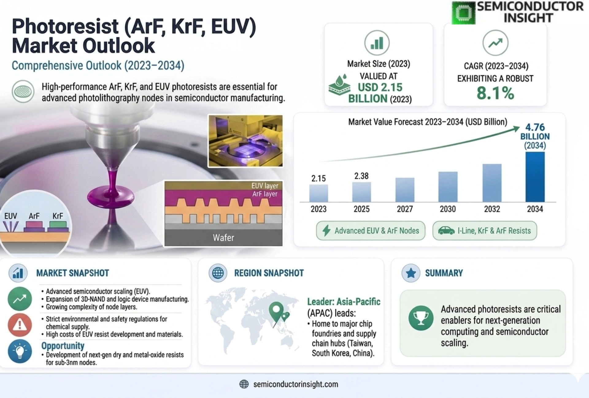
Global Photoresist (ArF, KrF, EUV) Market size was valued at USD 2.15 billion in 2023. The market is projected to grow from USD 2.38 billion in 2025 to USD 4.76 billion by 2034, exhibiting a CAGR of 8.1% during the forecast period.
Photoresists are light-sensitive materials used in semiconductor and microelectronics manufacturing to transfer circuit patterns onto substrates through photolithography processes. These specialized chemical formulations include ArF (Argon Fluoride), KrF (Krypton Fluoride), and EUV (Extreme Ultraviolet) variants, each tailored for specific wavelength exposures and resolution requirements. While KrF photoresists remain widely adopted for mature technology nodes, ArF immersion photoresists dominate advanced logic and memory chip production due to their superior resolution capabilities below 40nm. Meanwhile, EUV photoresists are gaining traction as the industry accelerates adoption of sub-7nm process technologies, driven by their ability to achieve finer patterning critical for next-generation semiconductor devices.
The market is experiencing robust expansion due to several converging factors, including the relentless pursuit of miniaturization in semiconductor manufacturing, surging demand for high-performance computing applications, and rapid proliferation of AI-driven hardware innovations. Furthermore, substantial investments in fab capacity expansions,particularly in Asia-Pacific,are amplifying consumption volumes across all photoresist categories. Industry collaborations are also shaping market dynamics; for instance, leading material suppliers such as Tokyo Ohka Kogyo Co., Ltd., JSR Corporation, and Shin-Etsu Chemical Co., Ltd., continue to advance R&D initiatives focused on enhancing sensitivity and defectivity performance metrics essential for cutting-edge lithography processes.
MARKET DRIVERS
Accelerated Semiconductor Scaling
As the demand for higher computational power drives Global Photoresist (ArF, KrF, EUV) Market forward, manufacturers are increasingly relying on extreme ultraviolet (EUV) lithography to push transistor densities beyond the 7nm node. This aggressive scaling requires specialized chemistries that can withstand intense radiation and ensure high-resolution patterning. Consequently, the transition from KrF to ArF and finally to EUV photoresists is a primary function driving market expansion in the semiconductor foundry sector.
Rise of Artificial Intelligence and HPC
The exponential growth in artificial intelligence, machine learning, and high-performance computing demands memory chips that utilize advanced patterning techniques. Photoresist (ArF, KrF, EUV) Market is directly benefiting from this ecosystem, as foundries seek to optimize throughput and reduce line-edge roughness. High-bandwidth memory manufacturing relies heavily on these specific photoresist formulations to achieve the necessary performance benchmarks.
➤ Advanced Packaging Integration
The adoption of heterogeneous integration allows for stacking different chips, which requires precise lithography solutions compatible with 3D structure stacking.
Furthermore, the continuous need for smaller circuit geometries fuels the demand for materials that offer superior thermal and chemical stability during wafer processing.
MARKET CHALLENGES
Material Sensitivity Issues
At nanometer-scale resolutions, maintaining photoresist material integrity becomes increasingly difficult as the market shifts toward EUV technology. Photoresist (ArF, KrF, EUV) Market faces significant hurdles in ensuring that chemistries remain stable under high-energy particle beams without forming defects or scattering off lattice structures.
Other Challenges
Technical Scalability
Scaling traditional DUV processes to support high-volume manufacturing of 3nm and 2nm nodes requires extensive modification of existing optical systems…
MARKET RESTRAINTS
Exorbitant R&D and Capital Costs
The capital intensity required for developing new photoresist formulations for Photoresist (ArF, KrF, EUV) Market is prohibitively high for smaller players, significantly limiting their ability to compete. The development cycle for next-generation chemistries is lengthy, and the failure rate during prototyping can lead to substantial financial losses for material suppliers.
Environmental and Regulatory Compliance
Strict regulations regarding hazardous materials used in photoresist processing, such as solvents and developers, often require costly changes to manufacturing facilities…
MARKET OPPORTUNITIES
Expansion into Automotive Applications
With the rapid digitization of automotive electronics and the push towards autonomous driving, the demand for high-reliability semiconductors is surging. This creates a significant opportunity for Photoresist (ArF, KrF, EUV) Market to diversify into automotive-grade lithography materials that ensure longevity and durability under extreme conditions.
➤ Back-End Processing Growth
Emerging technologies in 2.5D and 3D packaging require novel lithography capabilities, opening new revenue streams for material suppliers in the advanced packaging segment.
Trends
Technological Shift Toward Advanced Lithography
Photoresists are light-sensitive materials utilized in semiconductor and microelectronics manufacturing to transfer circuit patterns onto substrates. The overall market is experiencing robust expansion driven by the relentless pursuit of device miniaturization and the rising complexity of integrated circuits. The demand landscape requires specialized chemical formulations tailored for specific photolithography process stages. As manufacturers strive for higher density integration, the industry faces ongoing challenges regarding sensitivity and defectivity, necessitating continuous innovation in formulation design to ensure production efficiency and yield while supporting the transfer of complex circuit geometries.
Other Trends
Strategic Material Utilization across Process Nodes
The specialized chemical formulations included in this market comprise ArF (Argon Fluoride), KrF (Krypton Fluoride), and EUV (Extreme Ultraviolet) variants, each tailored for specific wavelength exposures and resolution requirements. KrF photoresists remain widely adopted for mature technology nodes within established manufacturing processes. Meanwhile, ArF immersion photoresists dominate advanced logic and memory chip production due to their superior resolution capabilities essential for advanced process nodes below 40nm. This segmentation ensures that manufacturers utilize the most appropriate material for their specific fabrication constraints. Furthermore, EUV photoresists are gaining traction as the industry accelerates adoption of next-generation semiconductor devices that require ultra-high resolution patterning.
Market Momentum and Infrastructure Investment
Market momentum is fueled by the surging demand for high-performance computing applications and the rapid proliferation of AI-driven hardware innovations. Furthermore, substantial investments in fab capacity expansions are amplifying consumption volumes across all photoresist categories globally. These capital inflows are particularly prevalent in Asia-Pacific regions where manufacturing facilities are expanding significantly. Industry collaborations are also shaping market dynamics, with leading material suppliers advancing R&D initiatives focused on enhancing sensitivity and defectivity performance metrics essential for cutting-edge lithography processes used in modern chip fabrication. This cooperation helps secure the supply chain for critical components used in both logic and memory applications.
COMPETITIVE LANDSCAPE
Key Industry Players
Leading material suppliers driving innovation in ArF, KrF, and EUV technologies
Global Photoresist (ArF, KrF, EUV) Market is a consolidated landscape dominated by a few major global material suppliers. The dominance of ArF immersion photoresists for advanced logic and memory production contrasts with the niche adoption of KrF photoresists for mature nodes. Market expansion is primarily fueled by aggressive fab capacity investments, particularly in the Asia-Pacific region, alongside the relentless pursuit of semiconductor miniaturization and AI-driven hardware innovations.
Industry dynamics are significantly shaped by ongoing collaborations among leading chemical suppliers focused on enhancing sensitivity and defectivity. These companies are advancing R&D initiatives to support the transition of EUV photoresists for sub-7nm process technologies, ensuring they meet the stringent performance requirements of cutting-edge lithography processes.
List of Key Semiconductor Companies Profiled
- Tokyo Ohka Kogyo Co., Ltd.
- JSR Corporation
- Shin-Etsu Chemical Co., Ltd.
- Dow Inc.
- Fujifilm Corporation
- SKC
- DuPont
- Brewer Science
- Merck KGaA (Darmstadt, Germany)
- HD Microsystems
Segment Analysis:
| Segment Category | Sub-Segments | Key Insights |
| By Type |
|
ArF Immersion currently dominates the market landscape due to its critical dimension control capabilities essential for manufacturing below 40nm features. It provides a robust solution for advanced logic and memory chips, offering superior adhesion and etch resistance while balancing cost-effectiveness compared to next-generation chemistries. The demand is largely driven by the semiconductor industry’s transition to high-k metal gate processes where precision is paramount. |
| By Application |
|
Logic Devices represent the leading application segment, requiring highly sensitive and defect-free materials to support complex transistor scaling. The push for 5G, AI, and high-performance computing continues to elevate the demand for advanced photoresists that can withstand aggressive etch processes without compromising patterning accuracy. Memory applications are also showing robust growth as manufacturers pursue 3D NAND and DRAM stacking technologies that demand exceptional uniformity across large wafers. |
| By End User |
|
Foundries currently drive significant consumption due to their high-volume capacity expansions, though Fabless companies are increasingly influencing material selection by mandating specific performance criteria for their future production nodes. IDCs focus on long-term vertical integration and material qualification to maintain consistency, while foundries prioritize process flexibility and yield enhancement to cater to diverse fabricator needs across different end markets. |
| By Wafer Size |
|
300mm Wafers are the leading segment as they are the standard substrate for advanced semiconductor manufacturing, hosting the majority of high-end processing lines. This size allows for higher throughput and cost-per-component reductions, making it the dominant platform for lithography processes. 200mm wafers remain relevant for certain analog, sensor, and legacy semiconductor production, creating a distinct niche market for specific photoresist formulations suited to lower thermal budgets and different processing environments. |
| By Process Node |
|
Advanced Process Nodes are the growth catalyst for the market, necessitating the adoption of cutting-edge photoresist chemistries for extreme ultraviolet lithography. These nodes require materials capable of handling high-dose exposure and producing minimal defects which is critical for sub-7nm structures. The migration from legacy nodes involves a complex supply chain evolution where manufacturers are investing heavily in R&D to manage the etch selectivity and chemical sensitivity challenges associated with thinner gate stacks and tighter line spaces. |
Regional Analysis: Photoresist (ArF, KrF, EUV) Market
The rapid adoption of Extreme Ultraviolet lithography in leading foundries within the region is pushing the boundaries of chip miniaturization, requiring photoresists that support high-sensitivity chemistries essential for sub-7nm nodes.
Strategic business maneuvers include the establishment of on-site chemical production capabilities to support local manufacturing clusters, thereby mitigating logistical risks and ensuring a steady flow of raw materials for the market.
Leading Japanese manufacturers hold a dominant position in the upstream supply of photoresist intermediates, catering to the downstream needs of domestic and international chip makers seeking high-grade materials.
The high volume of mobile devices and automotive chips produced in the region drives consistent consumption of both standard and advanced resins, creating a resilient demand baseline for the market through 2034.
North America
North America maintains a strong strategic position primarily through its high concentration of semiconductor design houses and fabless manufacturers, which drive the demand for next-generation photoresist materials. The business strategies adopted here focus heavily on R&D and intellectual property innovation, with a keen eye on maintaining technological leadership in chip architectures. While the volume of fabrication capacity is lower than in Asia, the demand for advanced Photoresist (ArF, KrF, EUV) Market materials remains critical for advanced packaging and logic technologies. The region continues to benefit from significant government investments in domestic chip manufacturing, ensuring that demand for high-resolution resists for cutting-edge nodes continues to rise steadily.
Europe
The European market is characterized by a specialized focus on industrial automation, automotive electronics, and legacy semiconductor maintenance, which sustains a steady consumption of photoresist materials. Regional players are heavily invested in developing materials that align with the high durability and environmental standards required for automotive and industrial applications. The business strategies in this region emphasize long-term partnerships and quality assurance, ensuring that the adoption of new photoresist technologies happens in a controlled, high-reliability context. As the automotive industry electrifies, the need for complex resist chemistries in power management units is growing, thereby reinforcing the demand withPhotoresist (ArF, KrF, EUV) Market ecosystem.
South America
South America presents a developing opportunity within the global landscape, driven by gradual infrastructure modernization and the adoption of smart technologies. The market here is still largely focused on cost-effective solutions and standard lithography materials suitable for mid-range semiconductor applications. Companies operating in this region tend to prioritize supply chain efficiency and competitive pricing to penetrate the market, leveraging strategic alliances with international suppliers. While the consumption volume is currently modest, the increasing digitalization of the region is projected to create a sustainable upward trend in demand over the next decade.
Middle East & Africa
The Middle East & Africa region is witnessing a nascent but growing interest in semiconductor manufacturing capabilities, driven by sovereign wealth funds and government initiatives aiming to diversify their economies. The market dynamics here are heavily influenced by global technology partnerships rather than indigenous production, resulting in a demand for standardized photoresist products used in industrial and scientific applications. As the region begins to explore localized chip manufacturing, the strategic focus is shifting towards establishing the necessary supply chains for essential materials, indicating a slow but promising trajectory for the wider Photoresist (ArF, KrF, EUV) Market in this geographic area.
Report Scope
This market research report provides a comprehensive analysis of the Photoresist (ArF, KrF, EUV) Market , covering the forecast period 2026–2034. It offers detailed insights into market dynamics, technological advancements, competitive landscape, and key trends shaping the industry.
Key focus areas of the report include:
- Market Overview: The report begins with an overview outlining its current market scenario, key growth indicators, and industry transformation drivers. It discusses macroeconomic factors, demand–supply balance, regulatory landscape, and the strategic role of semiconductors in powering advancements across industries such as automotive, telecommunications, consumer electronics, and industrial automation.
- Market Size & Forecast: Historical data and future projections for revenue, unit shipments, and market value across major regions and segments.
- Segmentation Analysis: Detailed breakdown by product type, technology, application, and end-user industry to identify high-growth segments and investment opportunities.
- Regional Insights: Insights into market performance across North America, Europe, Asia-Pacific, Latin America, and the Middle East & Africa, including country-level analysis where relevant.
- Competitive Landscape: Profiles of leading market participants, including their product offerings, R&D focus, manufacturing capacity, pricing strategies, and recent developments such as mergers, acquisitions, and partnerships.
- Technology Trends & Innovation: Assessment of emerging technologies, integration of AI/IoT, semiconductor design trends, fabrication techniques, and evolving industry standards.
- Market Drivers & Restraints: Evaluation of factors driving market growth along with challenges, supply chain constraints, regulatory issues, and market-entry barriers.
- Stakeholder Insights: Insights for component suppliers, OEMs, system integrators, investors, and policymakers regarding the evolving ecosystem and strategic opportunities.
Primary and secondary research methods are employed, including interviews with industry experts, data from verified sources, and real-time market intelligence to ensure the accuracy and reliability of the insights presented.
FREQUENTLY ASKED QUESTIONS:
What is the current market size of Photoresist (ArF, KrF, EUV) Market?
-> Global Photoresist (ArF, KrF, EUV) Market size was valued at USD 2.15 billion in 2023. The market is projected to grow from USD 2.38 billion in 2025 to USD 4.76 billion by 2034, exhibiting a CAGR of 8.1% during the forecast period.
Which key companies operate Photoresist (ArF, KrF, EUV) Market?
-> Key players include Tokyo Ohka Kogyo Co., Ltd., JSR Corporation, and Shin-Etsu Chemical Co., Ltd., among others.
What are the key growth drivers?
-> Key growth drivers include relentless pursuit of miniaturization in semiconductor manufacturing, surging demand for high-performance computing applications, and rapid proliferation of AI-driven hardware innovations.
Which region dominates the market?
-> Asia-Pacific dominates the market due to substantial investments in fab capacity expansions, while Europe remains a dominant market.
What are the emerging trends?
-> Emerging trends include EUV photoresists gaining traction as the industry accelerates adoption of sub-7nm process technologies.

Get Sample Report PDF for Exclusive Insights
Report Sample Includes
- Table of Contents
- List of Tables & Figures
- Charts, Research Methodology, and more...
 Download Sample Report PDF


