Lithography Equipment Market Insights
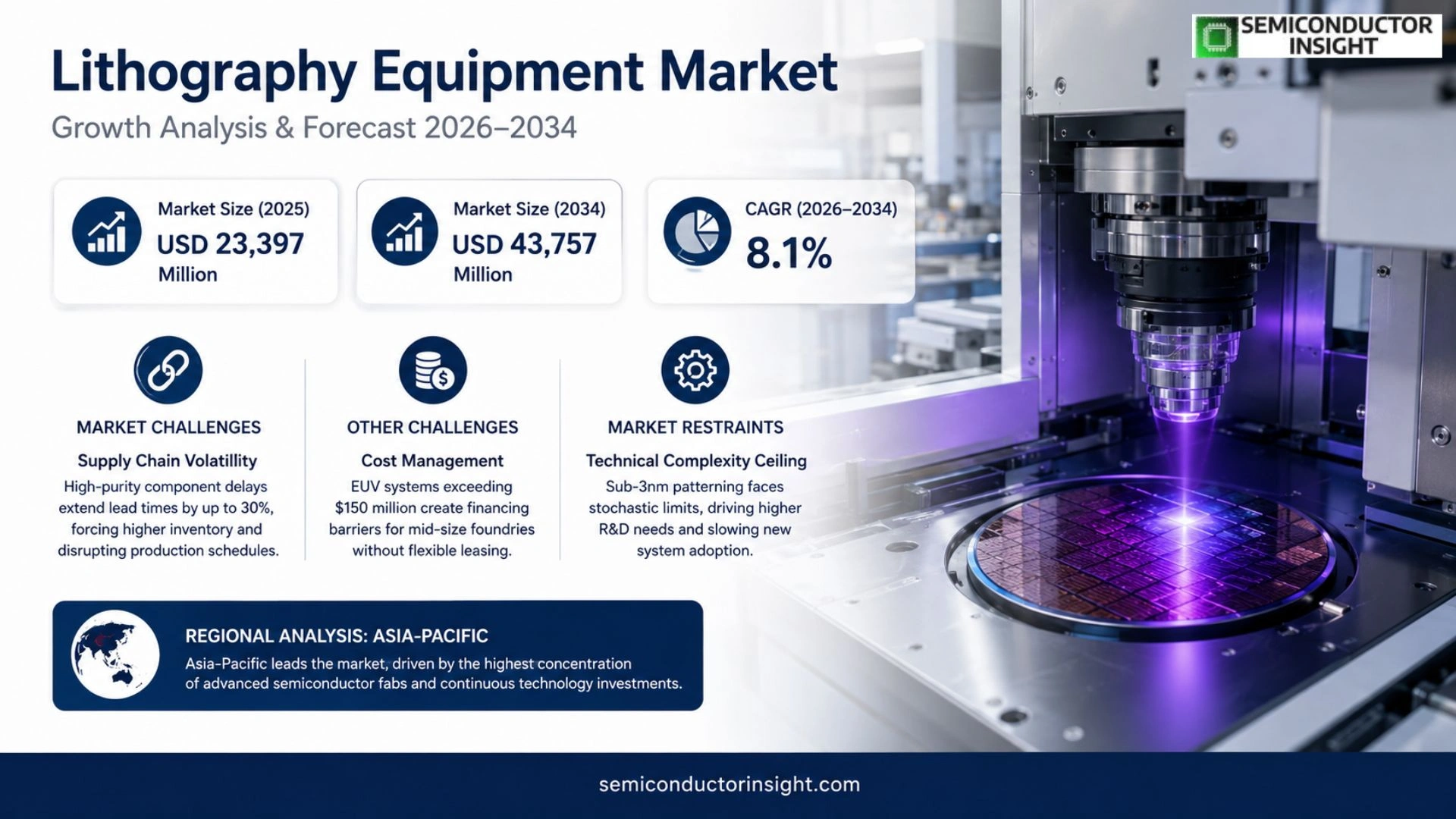
Lithography Equipment market size was valued at USD 23,397 million in 2025 and will rise to USD 43,757 million by 2034, reflecting a CAGR of 8.1% over the forecast period.
Lithography systems constitute the core patterning toolsets that transfer reticle (mask) designs onto photoresist, enabling subsequent steps such as etch, deposition and implantation. The scope covers semiconductor lithography,delivering sub‑nanometer resolution on silicon wafers,and flat‑panel‑display (FPD) lithography, which patterns large glass substrates for LCD and OLED production. A fast‑growing adjacency is advanced packaging, where lithography supports larger panels and tighter overlay for redistribution layers.
The market expands because AI‑driven HPC chips and high‑bandwidth memory increase wafer‑level lithography intensity, while geopolitical export controls tighten tool availability. Recent milestones include ASML’s first High‑NA EUV system delivery in 2024, Canon’s launch of the FPA‑8000iW platform for large‑panel i‑line stepping, and Nikon’s DSP‑100 initiative linking FPD large‑substrate capability with semiconductor‑grade imaging. These developments reinforce lithography equipment as a capacity‑constraining asset and a strategic lever for manufacturers.
MARKET DRIVERS
Technology Scaling Demands
The push for sub‑10‑nanometer patterning has forced chipmakers to replace legacy scanners with next‑generation systems. Lithography Equipment Market participants that can deliver sub‑resolution assist features are seeing order books swell, as manufacturers chase higher transistor densities without compromising yield.
Investment in EUV Infrastructure
Capital allocations to extreme‑ultraviolet (EUV) lines have crossed the $12 billion mark in the past year, reflecting confidence in the technology’s ability to sustain Moore’s Law. Companies that couple EUV sources with high‑throughput optics are positioning themselves as indispensable suppliers for fabs expanding beyond 5‑nm nodes.
➤ Strategic partnerships between equipment makers and photomask fabs are accelerating the adoption curve, turning what was once a niche capability into a mainstream requirement.
Finally, the emergence of high‑NA optics promises wider fields of view, translating into faster wafer throughput. Early adopters anticipate a measurable lift in weekly output, prompting them to lock in equipment purchases ahead of the next design cycle.
MARKET CHALLENGES
Supply Chain Volatility
Recent disruptions in high‑purity laser glass deliveries have extended lead times for critical components by up to 30 %. This lag forces fab managers to maintain higher safety stocks, eroding margin expectations and complicating production schedules.
Other Challenges
Cost Management
The capital intensity of EUV platforms,often exceeding $150 million per line,creates a financing hurdle for mid‑size foundries. Without flexible leasing structures, these players risk being locked out of the most advanced process nodes.
MARKET RESTRAINTS
Technical Complexity Ceiling
As patterning moves below 3 nm, stochastic effects in photon absorption become more pronounced, challenging the predictability of exposure results. Equipment vendors must invest heavily in simulation and metrology, stretching R&D budgets and limiting the speed at which new systems can be fielded.
MARKET OPPORTUNITIES
Retrofit Services for Legacy Scanners
Many fabs operate older 193‑nm scanners that, with targeted upgrades, can support intermediate nodes such as 7 nm. Providing modular retrofit kits opens a revenue stream that leverages existing asset bases while delivering incremental performance gains.
Emerging Materials Integration
Integrating new resist chemistries that exhibit higher EUV absorption efficiency can reduce dose requirements, translating into lower operational costs. Suppliers that co‑develop these materials with fab customers stand to capture a share of the ancillary market that grows in parallel with equipment sales.
Lithography Equipment Market Trends
Shift to High‑NA EUV and Large‑Panel Lithography
The emergence of High‑NA EUV tools marks the most visible change in Lithography Equipment market. ASML’s recent deliveries demonstrate that the technology is moving from laboratory prototypes to early‐stage production lines, enabling resolutions that reduce the need for multiple patterning steps. This transition matters because it directly lowers cycle time for leading‑edge logic nodes, giving chipmakers a clearer route to the next generation of AI and high‑performance computing devices. At the same time, Canon and Nikon are extending i‑line and KrF platforms to panel‑scale substrates, a response to the expanding demand for panel‑level advanced packaging. The combined effect is a bifurcated equipment portfolio where extreme‑wavelength tools serve the most advanced wafers while mature‑node scanners sustain volume production.
Other Trends
Advanced Packaging Integration
Panel‑level packaging (PLP) is reshaping the competitive calculus for lithography suppliers. Large‑area exposure systems such as Canon’s FPA‑8000iW and Nikon’s DSP‑100 are being positioned as essential assets for redistributing layers on motherglass substrates. The value of this capability is linked to the rising adoption of heterogeneous integration, where memory, logic, and RF blocks are assembled on a single panel. By providing higher overlay precision over a broad field, these tools help manufacturers meet the tighter alignment tolerances required for chiplets, thereby creating a new revenue stream that is less sensitive to the traditional wafer‑centric cycles.
FPD Scaling and OLED Demand
Flat‑panel display (FPD) lithography is undergoing a parallel upgrade driven by 4K/8K TV production and the shift toward OLED architectures. Larger motherglass formats,sometimes exceeding 10,000 mm²,are becoming the norm, prompting vendors to prioritize field size, stitching accuracy, and uniformity. This trend is amplified by the need for higher pixel density, which translates into tighter critical‑dimension control across the entire panel. For equipment manufacturers, the implication is twofold: engineering larger exposure optics while preserving semiconductor‑grade imaging fidelity, and aligning product roadmaps with the rapid refresh cycles of consumer electronics. The outcome is a more diversified Lithography Equipment Market where FPD and advanced packaging demand reinforce each other, reducing reliance on any single application segment.
COMPETITIVE LANDSCAPE
Key Industry Players
Lithography Equipment Market – Competitive Overview
ASML remains the singular supplier of high‑NA EUV platforms, a position that anchors its revenue stream and locks in a sizable portion of the market’s capital spending. The firm’s recent delivery of its first High‑NA EUV tools confirms a transition from prototype to serial production, creating a supply bottleneck that directly influences fab expansion plans for leading‑edge logic and memory nodes. Canon and Nikon, while unable to match ASML’s EUV footprint, command the DUV and i‑line segments with a portfolio that spans KrF, ArF immersion and large‑area panel scanners. Their equipment underpins mature‑node fabs and the fast‑growing advanced‑packaging sector, where overlay precision and throughput are decisive factors for cost‑effective redistribution‑layer formation.
Beyond the three tier‑1 vendors, a cadre of specialized manufacturers fills gaps in the ecosystem. SMEE supplies China‑focused KrF and i‑line tools, allowing domestic fabs to secure a degree of technological independence. Ultratech (under Veeco) and LEXTAR concentrate on niche FPD and printed‑circuit‑board lithography, leveraging small‑form‑factor steppers that excel in high‑resolution patterning of glass substrates. SUSS MicroTech offers laser‑direct‑write systems that support mask‑less prototyping for emerging display technologies. The legacy Cymer business, now integrated into ASML, continues to provide DUV light sources that sustain high‑volume production lines. Tokyo Electron supplies peripheral lithography components and retrofit kits, enhancing the lifecycle of older scanners and enabling cost‑effective upgrades for legacy fabs. Collectively, these players sustain a diversified supply chain, mitigate concentration risk, and create entry points for regional fab champions seeking differentiated capabilities.
List of Key Lithography Equipment Companies Profiled
- ASML
- Canon
- Nikon
- SMEE
- Ultratech (Veeco)
- LEXAR
- SUSS MicroTech
- Cymer
- Tokyo Electron (TEL)
- HOYA Corporation
- Nanotech Imaging
- GCA (General Scanning Inc.)
- MAXvision
- Fujifilm
- Rohm and Haas
Segment Analysis:
| Segment Category | Sub-Segments | Key Insights |
| By Type |
|
EUV Lithography drives the most advanced semiconductor nodes. • Provides the resolution required for leading‑edge logic and memory devices. • High‑NA EUV is emerging as the next platform shift, enabling lower multipatterning. • Supplier concentration makes it a strategic asset for fab operators. |
| By Application |
|
Front‑end wafer lithography remains the core demand driver for semiconductor fabs. • Supports scaling of logic and memory chips where overlay precision is critical. • Co‑exists with mature DUV tools to address specialty nodes. • Integration with computational lithography enhances pattern fidelity. |
| By End User |
|
Logic chips exert the highest lithography intensity. • AI and HPC workloads drive continual node shrink. • Require the most advanced overlay and CD control. • Pushes adoption of High‑NA EUV and advanced computational techniques. |
| By Technology Trend |
|
Computational lithography is reshaping pattern generation and mask design. • Enables finer feature placement without new hardware. • Reduces mask costs for complex nodes. • Enhances defect mitigation across EUV and DUV platforms. |
| By Market Driver |
|
AI & HPC demand fuels relentless scaling. • Drives higher lithography throughput and tighter overlay. • Encourages investment in next‑generation EUV tools. • Intensifies competition for limited equipment capacity. |
Regional Analysis: Lithography Equipment Market
Asia‑Pacific
EUV lithography has moved beyond pilot lines into volume production across Taiwan and Korea, prompting vendors to prioritize high‑NA development. The rapid migration to sub‑5‑nm processes forces equipment makers to integrate advanced metrology and alignment modules, raising the bar for system precision and uptime.
National semiconductor initiatives in China, Japan and Singapore allocate substantial capital toward domestic lithography capabilities. These programs incentivize joint‑ventures and technology transfer, creating a competitive pressure that pushes incumbents to offer more flexible financing and localized support structures.
Recent disruptions have driven manufacturers to diversify sources for high‑purity optics and laser assemblies. Collaborative inventory models between vendors and regional distributors now shorten lead times, allowing fabs to maintain wafer‑throughput targets despite global logistics volatility.
Established players leverage their legacy EUV platforms to secure long‑term service contracts, while emerging challengers focus on niche process nodes where cost‑effective alternatives to EUV can still deliver performance gains, reshaping the market share calculus.
North America
North America remains a hub for research‑driven lithography innovation, anchored by major R&D centers in the United States. While the region lags behind Asia‑Pacific in volume production, its emphasis on next‑generation high‑NA prototypes attracts a niche clientele seeking bespoke solutions. Federal investment in advanced manufacturing, coupled with a mature ecosystem of suppliers, supports a steady pipeline of pilot projects that test the limits of resolution enhancement techniques. Equipment firms that can translate these experimental gains into reliable, cost‑effective offerings stand to capture the premium segment of Lithography Equipment market in this geography.
Europe
European lithography players benefit from a tightly integrated supply chain that emphasizes precision engineering and sustainability. The region’s strategic focus on circular‑economy principles encourages equipment manufacturers to develop modular architectures that facilitate refurbishment and component reuse. Moreover, EU funding programs prioritize collaborative research across borders, fostering a culture of open innovation that accelerates adoption of novel illumination sources. As chipmakers in the automotive and industrial sectors strive for higher yields, Europe’s reputation for engineering excellence becomes a decisive factor in procurement decisions, reinforcing its position as a reliable albeit smaller market.
South America
South America’s lithography landscape is shaped by a gradual shift from assembly‑test operations toward modest fab establishments in Brazil and Chile. The market’s growth trajectory hinges on regional initiatives that aim to reduce reliance on imported semiconductor components. Although the current demand volume is limited, investors are attracted by the prospect of establishing a cost‑competitive production base backed by government incentives. Vendors that can tailor service models to accommodate smaller order sizes and provide on‑site training will likely secure early footholds in this emerging segment of Lithography Equipment market.
Middle East & Africa
In the Middle East & Africa, Lithography Equipment market is still in its nascent stage, driven primarily by strategic diversification efforts in the United Arab Emirates and South Africa. These countries are positioning themselves as regional hubs for semiconductor design and testing, leveraging tax‑free zones and partnerships with Asian manufacturers. While the immediate equipment requirement centers on mature‑node platforms, the long‑term vision includes building local expertise for advanced lithography processes. Companies that can offer turnkey solutions,including knowledge transfer and after‑sale support,will likely become preferred suppliers as the region’s ambitions mature.
Report Scope
This market research report provides a comprehensive analysis of the Lithography Equipment Market , covering the forecast period 2026–2034. It offers detailed insights into market dynamics, technological advancements, competitive landscape, and key trends shaping the industry.
Key focus areas of the report include:
- Market Overview: The report begins with an overview outlining its current market scenario, key growth indicators, and industry transformation drivers. It discusses macroeconomic factors, demand–supply balance, regulatory landscape, and the strategic role of semiconductors in powering advancements across industries such as automotive, telecommunications, consumer electronics, and industrial automation.
- Market Size & Forecast: Historical data and future projections for revenue, unit shipments, and market value across major regions and segments.
- Segmentation Analysis: Detailed breakdown by product type, technology, application, and end-user industry to identify high-growth segments and investment opportunities.
- Regional Insights: Insights into market performance across North America, Europe, Asia-Pacific, Latin America, and the Middle East & Africa, including country-level analysis where relevant.
- Competitive Landscape: Profiles of leading market participants, including their product offerings, R&D focus, manufacturing capacity, pricing strategies, and recent developments such as mergers, acquisitions, and partnerships.
- Technology Trends & Innovation: Assessment of emerging technologies, integration of AI/IoT, semiconductor design trends, fabrication techniques, and evolving industry standards.
- Market Drivers & Restraints: Evaluation of factors driving market growth along with challenges, supply chain constraints, regulatory issues, and market-entry barriers.
- Stakeholder Insights: Insights for component suppliers, OEMs, system integrators, investors, and policymakers regarding the evolving ecosystem and strategic opportunities.
Primary and secondary research methods are employed, including interviews with industry experts, data from verified sources, and real-time market intelligence to ensure the accuracy and reliability of the insights presented.
FREQUENTLY ASKED QUESTIONS:
What is the current market size of Lithography Equipment Market?
-> Lithography Equipment market will rise to USD 43,757 million by 2034, reflecting a CAGR of 8.1% over the forecast period.
Which key companies operate in Lithography Equipment Market?
-> Key players include ASML, Canon, Nikon, SMEE, among others.
What are the key growth drivers?
-> Key growth drivers include AI and high‑performance computing (HPC) demand, advanced memory expansion, increased lithography intensity per wafer, and geopolitical/export‑control factors influencing tool availability.
Which region dominates the market?
-> Asia-Pacific leads the market, driven by strong semiconductor manufacturing hubs in China, Japan, and South Korea, while also supporting extensive flat‑panel display and advanced‑packaging activities.
What are the emerging trends?
-> Emerging trends include High‑NA EUV deployment, larger‑motherglass panel lithography for OLED/4K‑8K production, and the convergence of semiconductor and FPD lithography platforms for advanced packaging applications.

Get Sample Report PDF for Exclusive Insights
Report Sample Includes
- Table of Contents
- List of Tables & Figures
- Charts, Research Methodology, and more...
 Download Sample Report PDF