Extreme Ultraviolet (EUV) Lithography Service Market Insights
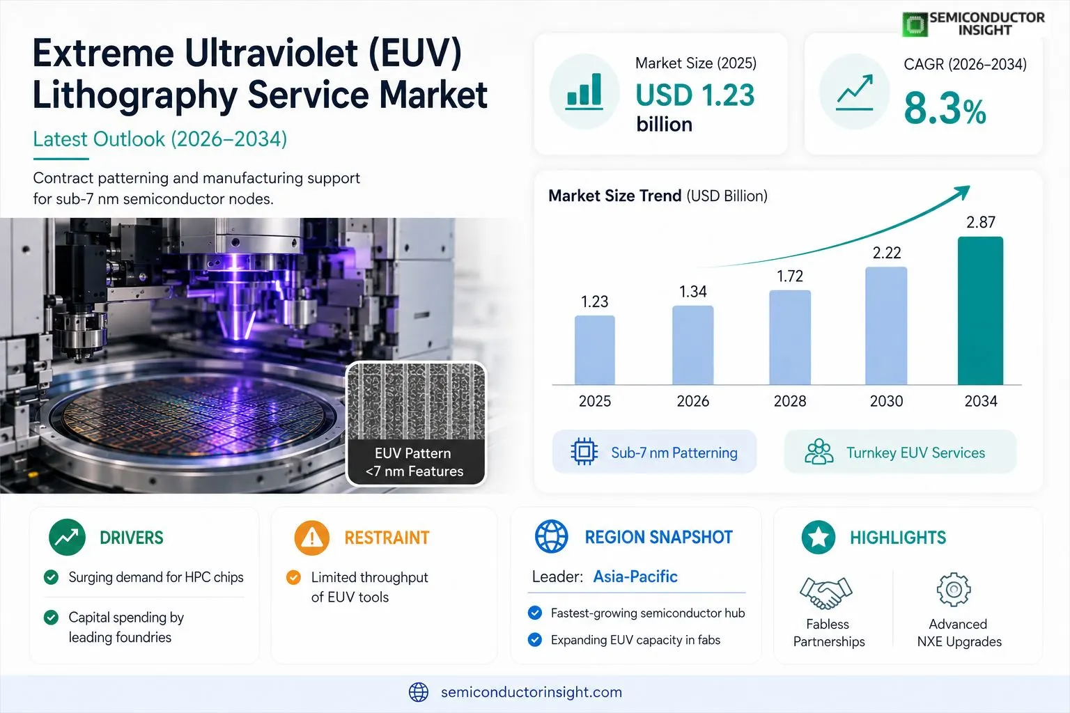
Global EUV lithography service market size was valued at USD 1.23 billion in 2025. The market is projected to grow from USD 1.34 billion in 2026 to USD 2.87 billion by 2034, exhibiting a CAGR of 8.3% during the forecast period.
EUV lithography services encompass contract patterning, mask repair, and high‑volume manufacturing support for sub‑7 nm semiconductor nodes using extreme ultraviolet wavelengths (~13.5 nm). These services enable chipmakers to achieve critical dimension control and throughput required for advanced logic, memory, and specialty processors.The market is accelerating because of surging demand for high‑performance computing chips, increased capital spending by leading foundries such as TSMC and Samsung, and continuous upgrades of ASML’s NXE platforms. Moreover, collaborations between equipment providers and fabless designers are driving adoption of turnkey EUV service models, while regional investments in semiconductor fabs across Asia‑Pacific further reinforce growth.
MARKET DRIVERS
Technology Adoption by Leading Foundries
The rapid adoption of Extreme Ultraviolet (EUV) lithography by major semiconductor foundries is driving demand for specialized service providers. Foundries such as TSMC and Samsung have integrated EUV steps into 5‑nm and 3‑nm production, creating a sustained need for outsourced EUV processing capacity.
Growth in High‑Performance Computing Applications
Expansion of AI, data‑center workloads, and edge computing requires chips with finer patterning, directly boosting Extreme Ultraviolet (EUV) Lithography Service Market as manufacturers seek cost‑effective access to EUV lines without building in‑house fabs.
➤ Industry analysts forecast a compound annual growth rate above 12% for EUV service revenue through 2032, reflecting continued capacity constraints at OEM fabs.
Regulatory incentives for domestic chip production in North America and Europe further encourage collaborations with EUV service firms, ensuring a diversified supply chain and reinforcing market momentum.
MARKET CHALLENGES
Capital Intensity of EUV Infrastructure
Deploying EUV scanners exceeds $150 million per unit, limiting the number of service providers able to compete. This high capital intensity creates entry barriers and concentrates capability among few players.
Other Challenges
Skilled Workforce Shortage
The niche expertise required to operate EUV tools leads to talent scarcity, slowing ramp‑up times for new service centers and increasing operational costs.
MARKET RESTRAINTS
Limited Throughput of Current EUV Tools
Even the latest EUV scanners achieve throughput rates below 100 wafers per hour for advanced nodes, restricting the volume of services that can be offered and capping revenue potential for providers.Maintenance downtime due to the delicate nature of laser‑generated plasma sources further reduces available capacity, making scheduling for external customers less predictable.
MARKET OPPORTUNITIES
Emerging Niche Nodes and Multi‑Patterning Services
As the industry moves toward sub‑2 nm logic, demand for multi‑patterning and mask‑less EUV services will rise, providing growth avenues for specialized service providers that can offer rapid prototyping and low‑volume production.Partnerships with equipment vendors to co‑develop next‑generation EUV sources, such as high‑NA (numerical aperture) scanners, present a strategic opportunity to capture early‑stage market share and differentiate service offerings.
Extreme Ultraviolet (EUV) Lithography Service Market Trends
Rising Demand for Sub‑7nm Nodes Drives Service Adoption
Extreme Ultraviolet (EUV) Lithography Service Market is experiencing a pronounced shift as semiconductor manufacturers target sub‑7 nm logic and memory layers. Chipmakers are accelerating capital programs to secure throughput that meets the stringent critical‑dimension control required for high‑performance computing, artificial‑intelligence accelerators, and advanced graphics processors. Leading foundries such as TSMC and Samsung are expanding capacity on ASML’s latest NXE platforms, which in turn creates a steady pipeline of contract patterning and mask‑repair workloads for service providers. The convergence of these technology drivers is translating into higher utilization of EUV service facilities, with customers favoring outsourced solutions to mitigate the steep upfront investment associated with in‑house EUV equipment.
Other Trends
Shift Toward Turnkey EUV Service Models
Service providers are increasingly packaging equipment, software, and expertise into turnkey offerings that enable fabless designers to access EUV patterning without developing internal expertise. Collaborative agreements between lithography equipment vendors and semiconductor design houses streamline the hand‑off of design data, reduce time‑to‑volume, and improve yield predictability. These models also incorporate post‑processing steps such as mask repair and defect mitigation, allowing customers to focus on product differentiation while leveraging specialized EUV expertise on a contractual basis.
Geographic Expansion of EUV Service Capacity in Asia‑Pacific
Regional investment in semiconductor fabs across the Asia‑Pacific is broadening the geographic footprint of EUV lithography services. New clean‑room expansions in Taiwan, South Korea, and Singapore are being equipped with high‑volume EUV lines, prompting service firms to establish satellite facilities close to major manufacturing hubs. This proximity reduces logistics latency, improves alignment with local supply chains, and supports the rapid scaling of advanced node production. As a result, Extreme Ultraviolet (EUV) Lithography Service Market is witnessing a balanced growth pattern where global demand is increasingly satisfied by regionally distributed service ecosystems.
COMPETITIVE LANDSCAPEKey Industry Players
Extreme Ultraviolet (EUV) Lithography Service Market – Competitive Overview
EUV lithography service market is anchored by a handful of dominant equipment manufacturers and integrated foundries that shape the supply chain for sub‑7 nm nodes. ASML Holding N.V. remains the sole supplier of high‑numerical‑aperture EUV scanners, controlling the critical upstream technology and driving the pace of platform upgrades that underpin service offerings. Complementing ASML, Taiwan Semiconductor Manufacturing Company (TSMC) operates an EUV service bureau that provides contract patterning and high‑volume manufacturing support to fabless designers, leveraging its extensive NXE‑3400B fleet. Samsung Electronics similarly delivers turnkey EUV services through its advanced fabs in South Korea, while Intel Corporation has begun offering limited EUV capacity to external customers as part of its IDM 2.0 strategy. These large players dictate pricing tiers, throughput standards, and the adoption curve for emerging chip architectures, creating a market structure where scale and equipment access are decisive competitive advantages.Beyond the headline manufacturers, a range of specialized players contribute niche capabilities that enhance the overall ecosystem. European research institutes such as IMEC and CEA‑LÉTI provide advanced mask repair and metrology services tailored to EUV patterns, often collaborating with equipment vendors on process optimization. SCREEN Semiconductor Solutions and Tokyo Electron offer peripheral tooling and lightweight EUV support services that enable smaller foundries to access the technology without full‑scale capital investment. Regional contract manufacturers like GlobalFoundries and United Microelectronics Corp. (UMC) have begun piloting EUV service modules for specific customers, while emerging service platforms from companies such as Lam Research and KLA focus on EUV‑specific inspection and defect mitigation, adding depth to the supply chain. These niche players collectively broaden market access and foster innovation across EUV service value chain.
List of Key EUV Lithography Service Companies Profiled
- ASML Holding N.V.
- Taiwan Semiconductor Manufacturing Company (TSMC)
- Samsung Electronics Co., Ltd.
- Intel Corporation
- GlobalFoundries Inc.
- IMEC (Interuniversity Microelectronics Centre)
- CEA‑LÉTI (Commissariat à l’Énergie Atomique – Laboratoire d’Etude des Technologies de l’Information)
- SCREEN Semiconductor Solutions
- Tokyo Electron Limited
- Lam Research Corporation
- KLA Corporation
- United Microelectronics Corporation (UMC)
- Advanced Semiconductor Engineering (ASE) Co., Ltd.
- Veeco Instruments Inc.
- Cymer (now part of ASML)
Segment Analysis:
| Segment Category | Sub-Segments | Key Insights |
| By Type |
|
Contract Patterning drives adoption due to its flexibility for emerging node designs.
|
| By Application |
|
Advanced Logic remains the primary growth engine for EUV services.
|
| By End User |
|
Foundry Service Providers lead the market by offering comprehensive EUV access.
|
| By Service Model |
|
Turnkey EUV Service is gaining traction as a preferred engagement model.
|
| By Technology Integration |
|
Technology Co‑Development stands out as a strategic catalyst.
|
Regional Analysis: North America
North America
The continuous advancement in EUV technology, including higher source power and improved optics, is a key driver for the service market. This necessitates specialized expertise for system maintenance, optimization, and troubleshooting.
The semiconductor industry is witnessing consolidation, leading to greater demand for integrated EUV service solutions from fewer, larger players. This trend presents both challenges and opportunities for service providers to adapt and scale their offerings.
Global supply chain complexities influence the availability and cost of EUV equipment and related services. Service providers need to navigate these challenges to ensure timely support and minimize disruptions for their clients.
Increasing emphasis on sustainable manufacturing practices is driving demand for energy-efficient EUV service solutions and responsible equipment lifecycle management.
United States
The United States represents a significant portion of the North American EUV Lithography Service Market, driven by a strong ecosystem of semiconductor manufacturers and research institutions. Government initiatives supporting domestic semiconductor production are further bolstering demand for these advanced services. The focus on developing leading-edge chips for defense, aerospace, and consumer electronics creates a stable and high-value market for EUV expertise.
Canada
Canada’s semiconductor sector, while smaller than the US, is experiencing steady growth and presents a niche market for EUV services. Collaboration between Canadian research labs and international companies is fostering innovation in lithography technologies, contributing to the regional market development.
Mexico
Mexico’s growing semiconductor industry, particularly in automotive and industrial applications, is beginning to explore EUV lithography services. The region’s strategic location and proximity to the US market offer opportunities for service providers to establish a foothold and cater to emerging demands.
Emerging Trends
The North American market is witnessing a trend towards predictive maintenance and remote monitoring of EUV systems. This shift is enabled by advancements in data analytics and artificial intelligence, allowing service providers to offer proactive support and minimize downtime for their clients.
Report Scope
This market research report provides a comprehensive analysis of the Extreme Ultraviolet (EUV) Lithography Service Market , covering the forecast period 2026–2034. It offers detailed insights into market dynamics, technological advancements, competitive landscape, and key trends shaping the industry.
Key focus areas of the report include:
- Market Overview: The report begins with an overview outlining its current market scenario, key growth indicators, and industry transformation drivers. It discusses macroeconomic factors, demand–supply balance, regulatory landscape, and the strategic role of semiconductors in powering advancements across industries such as automotive, telecommunications, consumer electronics, and industrial automation.
- Market Size & Forecast: Historical data and future projections for revenue, unit shipments, and market value across major regions and segments.
- Segmentation Analysis: Detailed breakdown by product type, technology, application, and end-user industry to identify high-growth segments and investment opportunities.
- Regional Insights: Insights into market performance across North America, Europe, Asia-Pacific, Latin America, and the Middle East & Africa, including country-level analysis where relevant.
- Competitive Landscape: Profiles of leading market participants, including their product offerings, R&D focus, manufacturing capacity, pricing strategies, and recent developments such as mergers, acquisitions, and partnerships.
- Technology Trends & Innovation: Assessment of emerging technologies, integration of AI/IoT, semiconductor design trends, fabrication techniques, and evolving industry standards.
- Market Drivers & Restraints: Evaluation of factors driving market growth along with challenges, supply chain constraints, regulatory issues, and market-entry barriers.
- Stakeholder Insights: Insights for component suppliers, OEMs, system integrators, investors, and policymakers regarding the evolving ecosystem and strategic opportunities.
Primary and secondary research methods are employed, including interviews with industry experts, data from verified sources, and real-time market intelligence to ensure the accuracy and reliability of the insights presented.
FREQUENTLY ASKED QUESTIONS:
What is the current market size of Extreme Ultraviolet (EUV) Lithography Service Market?
-> Extreme Ultraviolet (EUV) Lithography Service Market was valued at USD 1.23 billion in 2025 and is expected to reach USD 2.87 billion by 2034.
Which key companies operate in Extreme Ultraviolet (EUV) Lithography Service Market?
-> Key players include ASML, TSMC, Samsung.
What are the key growth drivers?
-> Key growth drivers include surging demand for high‑performance computing chips, increased capital spending by leading foundries, continuous upgrades of ASML’s NXE platforms, collaborations between equipment providers and fabless designers, and regional investments in Asia‑Pacific.
Which region dominates the market?
-> Asia‑Pacific is the fastest‑growing region and dominates market activity.
What are the emerging trends?
-> Emerging trends include turnkey EUV service models, collaborative equipment‑fabless partnerships, and expanding EUV capacity in Asia‑Pacific fabs.

Get Sample Report PDF for Exclusive Insights
Report Sample Includes
- Table of Contents
- List of Tables & Figures
- Charts, Research Methodology, and more...
 Download Sample Report PDF