
Key Statistics
Key Takeaways
- Market size and growth: USD 2.79 billion in 2025, rising to USD 5.13 billion by 2034 at a 7.0% CAGR over 2026–2034.
- Asia Pacific is the largest regional market in 2025, supported by the location of relevant manufacturing, customers and supply chains.
- EUV Photoresists is a core product segment, while newer or more integrated variants create higher-value growth opportunities.
- Analog represents an important application cluster because purchasing is directly linked to system performance and qualification requirements.
- Primary driver: More EUV exposures in advanced logic and memory raise demand for high-performance resist materials with strong sensitivity, resolution and defect control.
- Structural restraint: Trace contamination can create yield loss, so suppliers must invest heavily in raw-material control, filtration, packaging and clean manufacturing.
IC Photoresist Market Overview
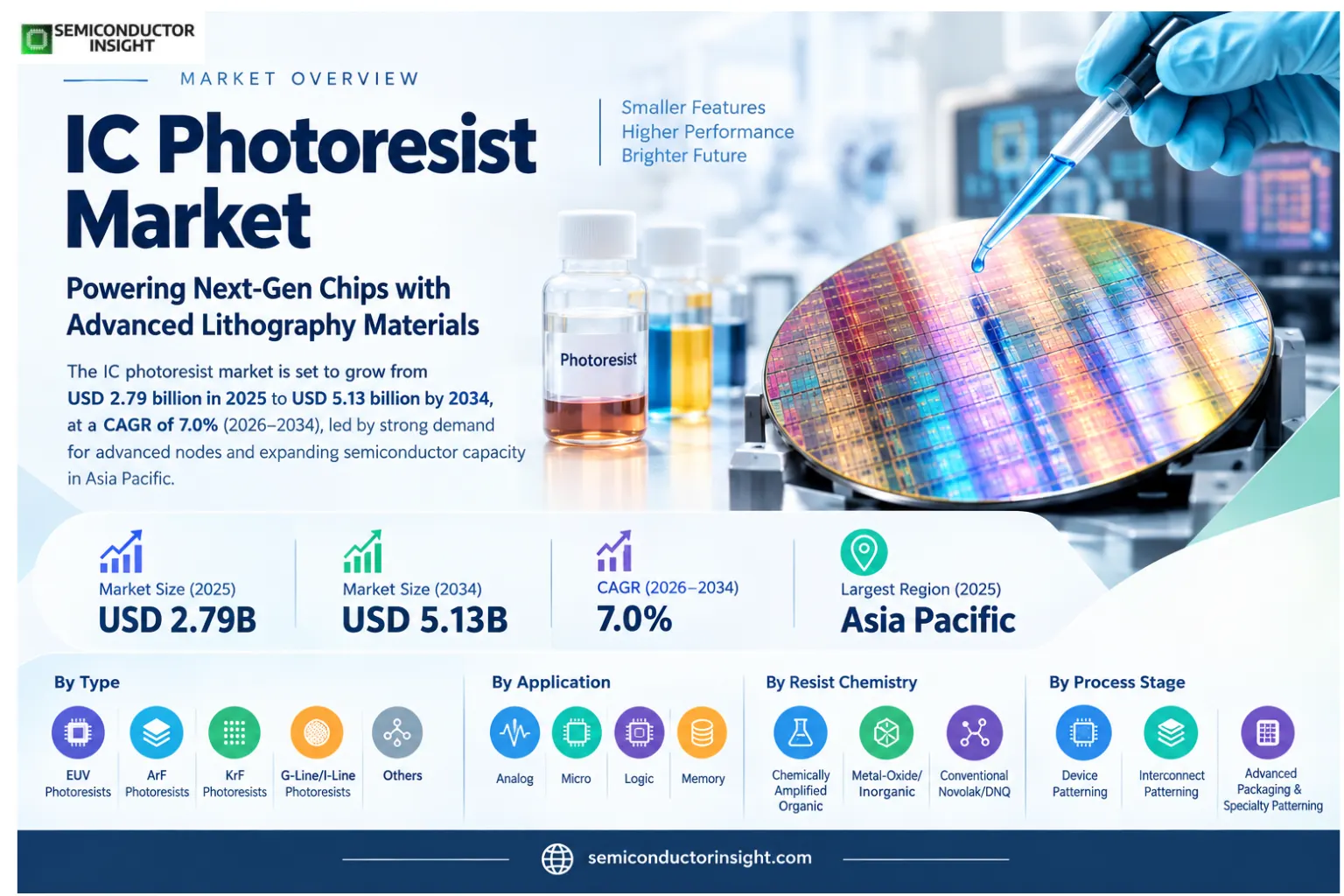
IC photoresist market was valued at USD 2.79 billion in 2025 and is projected to reach USD 5.13 billion by 2034, expanding at a CAGR of 7.0% during 2026–2034. Asia Pacific is the largest regional market in 2025.
IC photoresists are photosensitive materials used to transfer circuit patterns onto semiconductor wafers during lithography. Different exposure platforms require tailored resist chemistry: g/i-line products serve mature processes, KrF and ArF support progressively finer DUV patterning, and EUV resists address leading-edge nodes. Because lithography steps are repeated many times across front-end processing, resist purity, defectivity, sensitivity and process-window stability directly affect yield.
The market is structurally split between high-volume mature-node materials and faster-growing leading-edge resists. Tokyo Ohka Kogyo states that it offers a full lineup spanning g/i-line, KrF, ArF and EUV photoresists, while JSR highlights both chemically amplified and metal-oxide EUV materials. This broad technology range reflects customer demand for node-specific materials rather than a single universal resist platform.
Asia Pacific leads because Japan and South Korea host major resist suppliers while Taiwan, South Korea, China and Japan account for a large share of semiconductor wafer fabrication. The region’s combination of materials production and end-use fabs shortens qualification loops and supports local technical service. EUV adoption increases value per wafer, while mature-node capacity keeps large volumes of KrF and g/i-line products in production.
Segment Analysis: By Type
By type, the market is segmented into EUV Photoresists, ArF Photoresists, KrF Photoresists, G-Line/I-Line Photoresists, Others. Product selection reflects performance, integration requirements, qualification burden and total lifecycle economics. The leading categories benefit from established installed bases, while newer technologies gain share when they solve a measurable system constraint or reduce ownership cost.
| Type | Commercial role | Market position |
|---|---|---|
| EUV Photoresists | Fastest-value-growth category as leading-edge logic and advanced memory migrate to more EUV layers. Metal-oxide and chemically amplified platforms compete on resolution, sensitivity, roughness and defectivity. | Core / leading segment |
| ArF Photoresists | A major value segment for 193 nm lithography, including immersion processes used at advanced and intermediate nodes. Multi-patterning keeps ArF strategically important even as EUV expands. | High-growth segment |
| KrF Photoresists | Widely used for mature and intermediate processes where 248 nm lithography offers favorable cost and throughput. | Established / specialized segment |
| G-Line/I-Line Photoresists | Large installed-base demand in power semiconductors, analog, discrete and mature-node manufacturing. Volumes remain resilient because many devices do not require leading-edge patterning. | Established / specialized segment |
| Others | Includes specialty thick-film, e-beam and niche lithographic materials used in non-mainstream semiconductor processes. | Established / specialized segment |
Segment Analysis: By Application
By application, demand spans Analog, Micro, Logic, Memory. Purchasing behavior varies because operating conditions, product life, reliability thresholds and unit volumes differ by application. High-value applications emphasize qualification and engineering support, while high-volume uses add stronger cost and supply-continuity pressure.
| Application | Demand characteristics |
|---|---|
| Analog | Relies heavily on mature lithography nodes and long product lifecycles, supporting steady g/i-line and DUV resist demand. |
| Micro | Microprocessor and microcontroller production spans mature to advanced nodes, producing a mixed resist requirement across KrF, ArF and EUV. |
| Logic | The leading-edge logic segment is a major driver of EUV and advanced ArF materials because finer pitches and more complex patterning increase lithography intensity. |
| Memory | DRAM scaling and advanced memory investment support EUV and ArF demand, while NAND and peripheral circuitry maintain substantial DUV usage. |
By Resist Chemistry
| Resist Chemistry | Market relevance |
|---|---|
| Chemically Amplified Organic | Creates a distinct design, manufacturing or procurement requirement within the market. |
| Metal-Oxide/Inorganic | Creates a distinct design, manufacturing or procurement requirement within the market. |
| Conventional Novolak/DNQ | Creates a distinct design, manufacturing or procurement requirement within the market. |
By Process Stage
| Process Stage | Market relevance |
|---|---|
| Device Patterning | Creates a distinct design, manufacturing or procurement requirement within the market. |
| Interconnect Patterning | Creates a distinct design, manufacturing or procurement requirement within the market. |
| Advanced Packaging & Specialty Patterning | Creates a distinct design, manufacturing or procurement requirement within the market. |
Regional Analysis
Asia Pacific leads the IC Photoresist market in 2025. Regional demand differs according to manufacturing concentration, end-use investment, qualification practices and local supplier support. The largest region combines the strongest near-term demand base with established customers and supply-chain infrastructure, while other regions create opportunities around localization, research, specialty manufacturing or fast-growing end uses.
How does regional demand differ across the market?
Regional market structure is not simply a difference in size. Asia Pacific typically benefits from manufacturing density and electronics supply chains, North America from system design and advanced technology investment, Europe from specialized industrial and automotive applications, and emerging regions from selective infrastructure and localization projects. Supplier strategy therefore needs to account for qualification, service coverage, logistics and customer concentration in each geography.
| Region | Position | Growth outlook | Demand profile | What decides supplier selection |
|---|---|---|---|---|
| Asia Pacific | Largest / major | High | Manufacturing-led | Local qualification and scale |
| North America | Major | High-value | Design and investment-led | Engineering support and supply security |
| Europe | Established | Moderate | Specialty industrial-led | Quality, compliance and lifecycle support |
| South America | Emerging | Selective | Import-led | Landed cost and channel access |
| Middle East & Africa | Emerging | Selective | Project-led | Project timing and local support |
Competitive Landscape
The IC Photoresist market is shaped by qualification depth, process know-how and customer support rather than by price alone. Leading suppliers use installed-base relationships, intellectual property, manufacturing quality and field engineering to protect design wins. Competition is strongest when customers can qualify multiple technically comparable suppliers, while highly specialized applications remain concentrated among vendors with proven reliability records.
Large suppliers typically compete across several adjacent product families, allowing them to bundle technical support and simplify customer sourcing. Specialized companies compete by focusing on a narrower technology, material set or performance envelope. In both cases, the ability to maintain consistent quality during volume production is essential because a component or material change can require renewed process qualification.
Regional presence is also strategic. Customers increasingly value local application engineering, shorter repair or replenishment cycles and geographically diversified production. This favors suppliers that can combine global process standards with local service infrastructure close to major manufacturing clusters.
| Company | Competitive position | Primary basis of competition |
|---|---|---|
| Tokyo Ohka Kogyo (TOK) | Tier 1 / established | Competes through qualified products, technical support and customer integration. |
| JSR | Tier 1 / established | Competes through qualified products, technical support and customer integration. |
| Shin-Etsu Chemical | Tier 1 / established | Competes through qualified products, technical support and customer integration. |
| DuPont | Tier 1 / established | Competes through qualified products, technical support and customer integration. |
| Fujifilm | Established / specialized | Competes through qualified products, technical support and customer integration. |
| Sumitomo Chemical | Established / specialized | Competes through qualified products, technical support and customer integration. |
| Dongjin Semichem | Established / specialized | Competes through qualified products, technical support and customer integration. |
| Merck KGaA | Established / specialized | Competes through qualified products, technical support and customer integration. |
Companies Profiled
Tokyo Ohka Kogyo (TOK); JSR; Shin-Etsu Chemical; DuPont; Fujifilm; Sumitomo Chemical; Dongjin Semichem; Merck KGaA; Allresist; SK Materials Performance; Everlight Chemical; Shanghai Sinyang Semiconductor Materials; Jiangsu Nata Opto-electronic Material.
Production Capacity Analysis
Production capacity is constrained less by nominal factory floor space than by precision process capability, clean manufacturing, calibrated equipment and qualified upstream materials. Expanding output therefore requires more than adding assembly stations: suppliers must preserve contamination control, statistical process capability and traceability as volume increases. Capacity decisions are also influenced by the need to remain close to key customers and reduce logistics risk.
The strongest capacity additions are likely to follow major customer clusters. This favors Asia Pacific for high-volume electronics and semiconductor production, while the United States and Europe attract selective localization in strategic technologies. Suppliers that can duplicate qualified processes across regions gain resilience, but transferring a tightly controlled process between sites can itself require customer revalidation.
Market Dynamics
Photoresist demand is driven by wafer starts, the number of lithography layers per wafer and the value of the resist platform used at each node. Leading-edge scaling raises material performance requirements, while mature-node expansion sustains large-volume conventional resist consumption.
Market Drivers
Drivers Impact Analysis
| Driver | Impact | Why it matters |
|---|---|---|
| EUV layer growth | High | More EUV exposures in advanced logic and memory raise demand for high-performance resist materials with strong sensitivity, resolution and defect control. |
| Advanced-node fab investment | High | New leading-edge capacity expands consumption of EUV and ArF materials and increases the need for localized technical support. |
| Mature-node resilience | Medium-High | Power, analog, automotive and industrial devices keep KrF and g/i-line products commercially important even as leading-edge nodes advance. |
| Materials innovation | Medium-High | Metal-oxide resists, dry-resist integration and improved underlayers create new value pools around lithography process optimization. |
EUV layer growth
More EUV exposures in advanced logic and memory raise demand for high-performance resist materials with strong sensitivity, resolution and defect control. The commercial implication is stronger design-in activity for suppliers that can translate the technical requirement into reliable volume production and responsive customer support.
Advanced-node fab investment
New leading-edge capacity expands consumption of EUV and ArF materials and increases the need for localized technical support. The commercial implication is stronger design-in activity for suppliers that can translate the technical requirement into reliable volume production and responsive customer support.
Mature-node resilience
Power, analog, automotive and industrial devices keep KrF and g/i-line products commercially important even as leading-edge nodes advance. The commercial implication is stronger design-in activity for suppliers that can translate the technical requirement into reliable volume production and responsive customer support.
Materials innovation
Metal-oxide resists, dry-resist integration and improved underlayers create new value pools around lithography process optimization. The commercial implication is stronger design-in activity for suppliers that can translate the technical requirement into reliable volume production and responsive customer support.
Market Restraints
Restraints Impact Analysis
| Restraint | Impact | Commercial effect |
|---|---|---|
| Extreme purity requirements | High | Trace contamination can create yield loss, so suppliers must invest heavily in raw-material control, filtration, packaging and clean manufacturing. |
| Concentrated qualification | Medium | A small number of advanced fabs and lithography platforms control leading-edge adoption, making qualification technically demanding and commercially concentrated. |
| Geopolitical and localization risk | Medium | Resist supply is concentrated in a limited number of countries, encouraging customers and governments to pursue alternative local supply chains. |
Extreme purity requirements
Trace contamination can create yield loss, so suppliers must invest heavily in raw-material control, filtration, packaging and clean manufacturing. This restraint does not eliminate demand, but it changes the pace of adoption and favors suppliers with stronger balance sheets, technical data and established qualification histories.
Concentrated qualification
A small number of advanced fabs and lithography platforms control leading-edge adoption, making qualification technically demanding and commercially concentrated. This restraint does not eliminate demand, but it changes the pace of adoption and favors suppliers with stronger balance sheets, technical data and established qualification histories.
Geopolitical and localization risk
Resist supply is concentrated in a limited number of countries, encouraging customers and governments to pursue alternative local supply chains. This restraint does not eliminate demand, but it changes the pace of adoption and favors suppliers with stronger balance sheets, technical data and established qualification histories.
Market Opportunities
Metal-oxide EUV resists
Higher EUV absorption and different stochastic behavior create a pathway for next-generation patterning materials. The opportunity is strongest where the supplier can document a system-level benefit and support the customer through integration, qualification and scale-up.
Regional production expansion
Suppliers can reduce logistics risk and improve customer response by building production near major fab clusters in Korea, Taiwan, the United States and Europe. The opportunity is strongest where the supplier can document a system-level benefit and support the customer through integration, qualification and scale-up.
Power semiconductor materials
Growth in SiC and GaN devices supports specialty thick-film and mature-wavelength photoresists for high-voltage structures. The opportunity is strongest where the supplier can document a system-level benefit and support the customer through integration, qualification and scale-up.
Patterning ecosystem partnerships
Closer collaboration among resist, deposition, etch and lithography suppliers can improve process windows and accelerate qualification. The opportunity is strongest where the supplier can document a system-level benefit and support the customer through integration, qualification and scale-up.
Supply Chain Analysis
Stage 1 — High-purity monomers, polymers, photoacid generators, solvents and metal precursors: Value capture depends on process control, yield and the ability to meet downstream qualification requirements. Bottlenecks at this stage can propagate quickly because customers often depend on validated materials, calibrated components or approved production routes rather than interchangeable spot-market supply.
Stage 2 — Resist formulation, filtration, ultra-clean blending and analytical control: Value capture depends on process control, yield and the ability to meet downstream qualification requirements. Bottlenecks at this stage can propagate quickly because customers often depend on validated materials, calibrated components or approved production routes rather than interchangeable spot-market supply.
Stage 3 — Fab-side coating, bake, exposure, development and pattern transfer: Value capture depends on process control, yield and the ability to meet downstream qualification requirements. Bottlenecks at this stage can propagate quickly because customers often depend on validated materials, calibrated components or approved production routes rather than interchangeable spot-market supply.
Stage 4 — Waste recovery, chemical logistics and customer-specific technical service: Value capture depends on process control, yield and the ability to meet downstream qualification requirements. Bottlenecks at this stage can propagate quickly because customers often depend on validated materials, calibrated components or approved production routes rather than interchangeable spot-market supply.
Recent Developments
Report Scope & Segmentation
| Attribute | Coverage |
|---|---|
| Market | IC Photoresist |
| Base Year | 2025 |
| Estimated Year | 2026 |
| Forecast Period | 2026–2034 |
| 2025 Market Size | USD 2.79 billion |
| 2034 Projected Market Size | USD 5.13 billion |
| CAGR (2026–2034) | 7.0% |
| Largest Market in 2025 | Asia Pacific |
| By Type | EUV Photoresists, ArF Photoresists, KrF Photoresists, G-Line/I-Line Photoresists, Others |
| By Application | Analog, Micro, Logic, Memory |
| By Resist Chemistry | Chemically Amplified Organic, Metal-Oxide/Inorganic, Conventional Novolak/DNQ |
| By Process Stage | Device Patterning, Interconnect Patterning, Advanced Packaging & Specialty Patterning |
| Companies Profiled | Tokyo Ohka Kogyo (TOK), JSR, Shin-Etsu Chemical, DuPont, Fujifilm, Sumitomo Chemical, Dongjin Semichem, Merck KGaA, Allresist, SK Materials Performance, Everlight Chemical, Shanghai Sinyang Semiconductor Materials, Jiangsu Nata Opto-electronic Material |
| Regions | North America; Europe; Asia Pacific; South America; Middle East & Africa |
Frequently Asked Questions
What is the IC Photoresist market size in 2025?
The global IC Photoresist market is valued at USD 2.79 billion in 2025.
What is the projected IC Photoresist market size by 2034?
The market is projected to reach USD 5.13 billion by 2034.
What is the CAGR of the IC Photoresist market from 2026 to 2034?
The market is projected to expand at a 7.0% CAGR during 2026–2034.
Which region leads the IC Photoresist market?
Asia Pacific is the largest market in 2025.
What are the main product types?
EUV Photoresists, ArF Photoresists, KrF Photoresists, G-Line/I-Line Photoresists, Others.
What are the key applications?
Analog, Micro, Logic, Memory.
What is the main growth driver?
More EUV exposures in advanced logic and memory raise demand for high-performance resist materials with strong sensitivity, resolution and defect control.
What is the main restraint?
Trace contamination can create yield loss, so suppliers must invest heavily in raw-material control, filtration, packaging and clean manufacturing.
Where are the strongest opportunities?
Higher EUV absorption and different stochastic behavior create a pathway for next-generation patterning materials. Suppliers can reduce logistics risk and improve customer response by building production near major fab clusters in Korea, Taiwan, the United States and Europe.
Which companies are active in the market?
Tokyo Ohka Kogyo (TOK), JSR, Shin-Etsu Chemical, DuPont, Fujifilm, Sumitomo Chemical, Dongjin Semichem, Merck KGaA are among the companies active in the market.
Research Sources & Evidence Base
View primary and official sources used in this overview
- Tokyo Ohka Kogyo — Semiconductor Manufacturing Field. Photoresist product range and lithography role.
- JSR — Sustainability 2025 – EUV Photoresists. EUV and metal-oxide-resist technology context.
- JSR / Inpria / Entegris — Cross-Licensing to EUV Lithography. Metal-oxide-resist development.
- Tokyo Ohka Kogyo — New Pyeongtaek Plant. Regional photoresist manufacturing expansion.

Get Sample Report PDF for Exclusive Insights
Report Sample Includes
- Table of Contents
- List of Tables & Figures
- Charts, Research Methodology, and more...
 Download Sample Report PDF




