MARKET INSIGHTS
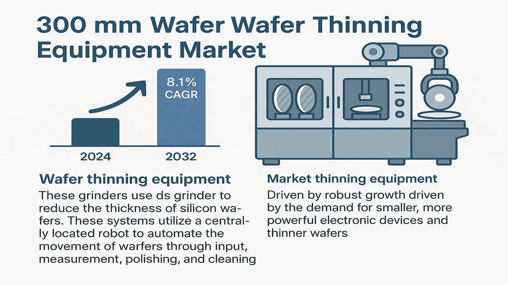
The global 300 mm Wafer Wafer Thinning Equipment Market was valued at 789 million in 2024 and is projected to reach US$ 1371 million by 2032, at a CAGR of 8.1% during the forecast period.
Wafer thinning equipment, also referred to as grinders, are precision machines used in semiconductor manufacturing to reduce the thickness of silicon wafers. These systems utilize a centrally located robot to automate the movement of wafers through a sequence of stations, including input, measurement, polishing, and cleaning. This process is critical for enabling the production of thinner, more advanced semiconductor devices that require high performance and miniaturization.
The market is experiencing robust growth driven by the relentless demand for smaller, more powerful electronic devices and the subsequent need for thinner wafers. The Asia-Pacific region dominates consumption, accounting for approximately 78% of the global market share, because of its strong semiconductor manufacturing base in countries like China, Japan, South Korea, and Taiwan. Furthermore, fully automatic equipment leads the product segment, holding about 53% of the market, as it offers superior precision and efficiency for high-volume production. Key industry players, including Disco, TOKYO SEIMITSU, and Okamoto, continue to innovate to meet the stringent requirements of modern semiconductor fabrication.
MARKET DYNAMICS
MARKET DRIVERS
Technological Advancements in Semiconductor Manufacturing to Drive Market Expansion
The global semiconductor industry is undergoing rapid technological evolution, driven by the demand for smaller, more powerful, and energy-efficient electronic devices. This evolution necessitates thinner wafers with higher precision, which directly fuels the adoption of advanced 300 mm wafer thinning equipment. Fully automatic systems, which account for approximately 53% of the market, are particularly favored due to their ability to handle larger volumes while maintaining stringent quality standards. Recent innovations include enhanced robotic handling, real-time thickness monitoring, and improved polishing techniques that reduce wafer breakage and improve yield rates. The shift towards nodes below 10nm and the increasing adoption of 3D packaging technologies further amplify the need for precision thinning solutions, making this equipment indispensable in modern fabs.
Surge in Semiconductor Demand Across Key Industries to Boost Market Growth
The semiconductor market is experiencing unprecedented growth, propelled by rising demand from computing, communication, automotive, and IoT applications. Global semiconductor sales have consistently exceeded historical averages, with particular strength in the Asia-Pacific region, which holds about 78% of the 300 mm wafer thinning equipment market. The automotive sector’s transition towards electric and autonomous vehicles requires advanced chips, while the expansion of 5G infrastructure and data centers further drives wafer demand. This surge necessitates higher production volumes and more efficient manufacturing processes, positioning wafer thinning equipment as a critical enabler of semiconductor scalability and performance.
Furthermore, increasing investments in semiconductor fabrication facilities, especially in leading regions like Taiwan, South Korea, and China, are accelerating equipment procurement. National initiatives aimed at strengthening semiconductor self-sufficiency are also contributing to market momentum, creating a robust pipeline for thinning equipment demand over the forecast period.
MARKET RESTRAINTS
High Initial Investment and Operational Costs to Limit Market Penetration
While the market for 300 mm wafer thinning equipment is expanding, high capital expenditure remains a significant barrier, particularly for smaller semiconductor manufacturers and emerging markets. Fully automatic systems, which dominate the market, involve substantial upfront costs not only for acquisition but also for installation, calibration, and integration into existing production lines. Operational expenses, including maintenance, consumables, and energy consumption, add to the total cost of ownership. These financial demands can deter smaller players from investing in state-of-the-art equipment, leading them to opt for semi-automatic or refurbished alternatives, thereby restraining overall market growth.
Technological Complexity and Skill Shortages to Hinder Adoption Rates
The operation and maintenance of advanced 300 mm wafer thinning equipment require highly specialized technical knowledge, creating adoption challenges in regions with limited access to skilled engineers and technicians. These systems involve complex robotics, precision mechanics, and sophisticated software, necessitating continuous training and support. A shortage of qualified personnel, compounded by an aging workforce in key semiconductor hubs, can lead to increased downtime, reduced efficiency, and higher operational risks. This skills gap is particularly acute in emerging semiconductor markets, where local expertise may not yet be fully developed, slowing the pace of technological adoption and market expansion.
MARKET OPPORTUNITIES
Expansion of Semiconductor Production Capacities to Unlock New Growth Avenues
Global initiatives to expand semiconductor manufacturing capabilities present significant opportunities for the 300 mm wafer thinning equipment market. Countries and regions are investing heavily in new fabrication plants and capacity upgrades to mitigate supply chain risks and meet rising demand. For example, major economies are rolling out substantial subsidies and policy support to bolster domestic chip production. This expansion drive is expected to increase the installation of advanced thinning equipment, particularly fully automatic systems, which are essential for high-volume, high-precision manufacturing. Partnerships between equipment suppliers and semiconductor makers to co-develop next-generation thinning technologies will further accelerate market growth.
Innovation in Equipment Design and Functionality to Create Competitive Advantages
Ongoing R&D efforts aimed at enhancing the efficiency, reliability, and versatility of wafer thinning equipment are opening new opportunities. Innovations such as integrated metrology, AI-driven process optimization, and reduced environmental footprint are becoming key differentiators. Manufacturers that successfully develop equipment with higher throughput, lower defect rates, and better compatibility with emerging materials like silicon carbide and gallium nitride will gain a competitive edge. Additionally, the trend towards modular and upgradable systems allows for easier integration and future-proofing, appealing to a broader range of customers and driving sustained market expansion.
MARKET CHALLENGES
Intense Competitive Pressure and Rapid Technological Obsolescence to Challenge Market Players
The 300 mm wafer thinning equipment market is characterized by intense competition among established players and the constant threat of technological obsolescence. Manufacturers must continuously innovate to keep pace with evolving semiconductor processes, which often requires significant R&D investment and short product life cycles. The rapid advancement of alternative technologies, such as wafer bonding and etching, also poses a challenge, as they could potentially reduce the reliance on mechanical thinning. Moreover, price competition, especially from regional suppliers, pressures profit margins and necessitates efficient cost management and strategic positioning to maintain market share.
Other Challenges
Supply Chain Vulnerabilities
Global supply chain disruptions can delay the production and delivery of thinning equipment, affecting market stability. Dependencies on specialized components, such as high-precision motors and sensors, from limited sources exacerbate these risks, requiring robust supply chain strategies.
Stringent Performance and Reliability Standards
Semiconductor manufacturers demand exceptionally high levels of equipment reliability and performance to minimize production downtime and maximize yield. Meeting these stringent standards consistently across diverse operational environments remains a persistent challenge for equipment providers.
300 MM WAFER WAFER THINNING EQUIPMENT MARKET TRENDS
Technological Advancements in Semiconductor Manufacturing to Emerge as a Trend in the Market
Technological advancements in semiconductor manufacturing are significantly driving the adoption of advanced 300 mm wafer thinning equipment. As the industry pushes towards smaller process nodes—now commonly below 10 nanometers—the demand for thinner wafers with higher precision has intensified. Fully automatic systems, which currently hold over 53% of the global market share, are increasingly favored because they integrate robotics, real-time metrology, and automated handling to achieve thicknesses as low as 50 micrometers while maintaining exceptional flatness and minimal subsurface damage. Recent innovations include the integration of AI-driven predictive maintenance and adaptive process control, which enhance yield rates and reduce operational downtime. Because these systems are critical for manufacturing advanced memory and logic devices, their development is closely tied to the broader semiconductor industry’s roadmap, which emphasizes performance and energy efficiency.
Other Trends
Miniaturization of Electronic Devices
The global trend towards miniaturization in electronics is a primary catalyst for the 300 mm wafer thinning equipment market. Consumer demand for thinner, lighter, and more powerful devices—such as smartphones, wearables, and IoT sensors—requires semiconductor wafers to be ground to increasingly precise thicknesses. While traditional thinning processes sufficed for older technology nodes, current applications often necessitate wafers thinner than 100 micrometers, especially for 3D IC stacking and through-silicon via (TSV) technologies. This trend is accelerating the shift from semi-automatic to fully automatic thinning systems, which offer the consistency and throughput needed for high-volume production. Furthermore, the rise of electric vehicles and advanced driver-assistance systems (ADAS) is introducing new requirements for robust, thin wafers in automotive semiconductors, further expanding the application scope for these precision tools.
Surge in Semiconductor Demand and Regional Manufacturing Expansion
A significant surge in global semiconductor demand, particularly across the computing, telecommunications, and automotive sectors, is propelling the 300 mm wafer thinning equipment market. The Asia-Pacific region dominates consumption, accounting for approximately 78% of the global market, driven by massive semiconductor fabrication facilities in Taiwan, South Korea, and China. This regional concentration is due to both established supply chains and substantial investments in new foundries and IDM (Integrated Device Manufacturer) capacity. However, other regions are also expanding; for example, new fabrication plants in the United States and Europe are beginning to adopt these advanced thinning systems to support domestic semiconductor resilience initiatives. This geographic expansion, coupled with the ongoing global chip shortage, has accelerated capital expenditures in wafer thinning equipment, with projections indicating the market will grow from $789 million in 2024 to $1371 million by 2032.
COMPETITIVE LANDSCAPE
Key Industry Players
Companies Strive to Strengthen their Product Portfolio to Sustain Competition
The competitive landscape of the global 300 mm wafer thinning equipment market is semi-consolidated, characterized by a mix of established multinational corporations and specialized regional manufacturers. Disco Corporation is a dominant force in this sector, commanding a significant market share due to its technologically advanced grinding and polishing systems and its entrenched presence in the Asia-Pacific region, which accounts for approximately 78% of global consumption. The company’s leadership is further solidified by its continuous innovation in fully automatic systems, which hold over 53% of the market.
TOKYO SEIMITSU (also known as ACM Research) and Okamoto Semiconductor Equipment Division are also major contenders, holding substantial shares. Their growth is largely driven by the robust semiconductor manufacturing ecosystems in Japan and South Korea, coupled with their ability to deliver high-precision equipment that meets the stringent requirements of integrated device manufacturers (IDMs) and foundries for advanced technology nodes.
Additionally, these leading companies are aggressively pursuing growth through strategic expansions, particularly in emerging semiconductor hubs, and through the launch of next-generation thinning systems designed for higher throughput and yield. This focus on innovation and geographical penetration is expected to further consolidate their market positions over the forecast period.
Meanwhile, other players like G&N Genauigkeitstechnik Nürnberg GmbH and CETC (China Electronics Technology Group Corporation) are strengthening their global footprint through significant investments in research and development and by forming strategic partnerships. These initiatives are aimed at capturing a larger share of the growing demand, especially from cost-sensitive markets and for specific application segments.
List of Key 300 mm Wafer Thinning Equipment Companies Profiled
- Disco Corporation (Japan)
- TOKYO SEIMITSU (Japan)
- G&N Genauigkeitstechnik Nürnberg GmbH (Germany)
- Okamoto Semiconductor Equipment Division (Japan)
- CETC (China Electronics Technology Group Corporation) (China)
- Koyo Machinery (Japan)
- SpeedFam (Japan)
- TSD (Taiwan)
- NTS (Korea)
Segment Analysis:
By Type
Fully Automatic Segment Dominates the Market Due to Superior Precision and High-Volume Production Capabilities
The market is segmented based on type into:
- Fully Automatic
- Semi Automatic
By Application
Foundry Segment Leads Due to High-Volume Outsourced Semiconductor Manufacturing
The market is segmented based on application into:
- IDM (Integrated Device Manufacturer)
- Foundry
By Technology
Grinding Technology Holds Prominence as the Primary Method for Bulk Material Removal
The market is segmented based on technology into:
- Grinding
- Chemical Mechanical Polishing (CMP)
- Dry Polishing
- Others (including Plasma Etching)
By Equipment Stage
Dual-Side Grinding Equipment Gains Traction for Enhanced Wafer Strength and Performance
The market is segmented based on equipment stage into:
- Back Grinding Equipment
- Dual-Side Grinding Equipment
- Polishing Equipment
- Cleaning and Drying Equipment
Regional Analysis: 300 mm Wafer Thinning Equipment Market
Asia-Pacific
The Asia-Pacific region dominates the global 300 mm wafer thinning equipment market, accounting for approximately 78% of global consumption. This leadership position is driven by the concentration of major semiconductor manufacturing hubs in countries like Taiwan, South Korea, Japan, and China. The region’s dominance is underpinned by massive investments in new fabrication plants (fabs) and the expansion of existing facilities by industry giants such as TSMC, Samsung, and SK Hynix. The relentless push towards advanced technology nodes below 10nm necessitates ultra-precise wafer thinning processes, creating sustained demand for high-end, fully automated equipment. While cost sensitivity remains a factor for some smaller foundries, the overarching trend is a strong preference for automation to ensure yield and meet the high-volume production requirements of the global electronics supply chain.
North America
North America represents a significant and technologically advanced market, primarily fueled by domestic IDMs (Integrated Device Manufacturers) like Intel and major R&D activities. The market is characterized by a high adoption rate of fully automatic systems due to the region’s focus on cutting-edge innovation and the high cost of labor. Recent U.S. government initiatives, including the CHIPS and Science Act which allocates billions in funding for domestic semiconductor production, are expected to catalyze new investments in fab equipment, including thinning systems. The presence of leading equipment suppliers and a strong ecosystem for semiconductor R&D further supports market growth, with a emphasis on equipment that offers superior precision, integration with other process steps, and advanced data analytics capabilities.
Europe
Europe’s market is more niche but remains critical, supported by a strong automotive and industrial semiconductor sector and the presence of key research institutions like IMEC. Demand is driven by specialized applications requiring high reliability, such as power semiconductors and sensors for automotive applications. European IDMs and foundries are significant investors in semi-automatic and fully automatic equipment to enhance their manufacturing capabilities for these specialized chips. Furthermore, stringent EU regulations on manufacturing precision and environmental standards encourage the adoption of advanced, efficient equipment that minimizes waste and energy consumption. Collaborative projects between industry and academia often serve as early adoption sites for next-generation thinning technologies.
South America
The market in South America is in its early stages of development. Current demand is limited and primarily serves regional electronics assembly needs rather than advanced semiconductor fabrication. The high capital investment required for 300 mm wafer thinning equipment is a significant barrier, leading to a greater reliance on imported thinned wafers or older-generation, refurbished equipment. While countries like Brazil have some local assembly operations, the lack of a mature domestic semiconductor manufacturing ecosystem and economic volatility restrain any substantial market growth for this advanced machinery in the near term.
Middle East & Africa
This region currently represents the smallest share of the global market. While there are long-term strategic ambitions in some Gulf nations to diversify into technology manufacturing, these are yet to materialize into significant demand for front-end semiconductor equipment like wafer thinners. Any existing demand is typically met through partnerships with established Asian or European foundries or through the import of finished semiconductor products. The market’s development is hindered by the absence of a local supply chain, a shortage of specialized technical expertise, and the overwhelming capital intensity required to establish a competitive semiconductor fabrication facility.
Report Scope
This market research report provides a comprehensive analysis of the global and regional Semiconductor and Electronics markets, covering the forecast period 2025–2032. It offers detailed insights into market dynamics, technological advancements, competitive landscape, and key trends shaping the industry.
Key focus areas of the report include:
- Market Size & Forecast: Historical data and future projections for revenue, unit shipments, and market value across major regions and segments.
- Segmentation Analysis: Detailed breakdown by product type, technology, application, and end-user industry to identify high-growth segments and investment opportunities.
- Regional Outlook: Insights into market performance across North America, Europe, Asia-Pacific, Latin America, and the Middle East & Africa, including country-level analysis where relevant.
- Competitive Landscape: Profiles of leading market participants, including their product offerings, R&D focus, manufacturing capacity, pricing strategies, and recent developments such as mergers, acquisitions, and partnerships.
- Technology Trends & Innovation: Assessment of emerging technologies, integration of AI/IoT, semiconductor design trends, fabrication techniques, and evolving industry standards.
- Market Drivers & Restraints: Evaluation of factors driving market growth along with challenges, supply chain constraints, regulatory issues, and market-entry barriers.
- Stakeholder Analysis: Insights for component suppliers, OEMs, system integrators, investors, and policymakers regarding the evolving ecosystem and strategic opportunities.
Primary and secondary research methods are employed, including interviews with industry experts, data from verified sources, and real-time market intelligence to ensure the accuracy and reliability of the insights presented.
FREQUENTLY ASKED QUESTIONS:
What is the current market size of Global 300 mm Wafer Thinning Equipment Market?
-> 300 mm Wafer Wafer Thinning Equipment Market was valued at 789 million in 2024 and is projected to reach US$ 1371 million by 2032, at a CAGR of 8.1% during the forecast period.
Which key companies operate in Global 300 mm Wafer Thinning Equipment Market?
-> Key players include Disco, TOKYO SEIMITSU, Okamoto Semiconductor Equipment Division, G&N, CETC, Koyo Machinery, SpeedFam, TSD, and NTS, among others.
What are the key growth drivers?
-> Key growth drivers include technological advancements in semiconductor manufacturing, the miniaturization of electronic devices, a surge in semiconductor demand, and the industry-wide shift towards fully automated solutions.
Which region dominates the market?
-> Asia-Pacific is the dominant region, holding approximately 78% of the global market share, driven by a robust semiconductor manufacturing ecosystem in countries like China, Japan, South Korea, and Taiwan.
What are the emerging trends?
-> Emerging trends include the increasing adoption of fully automatic systems, which accounted for 53% of the market in 2024, and the integration of advanced robotics and AI for enhanced precision and throughput.

Get Sample Report PDF for Exclusive Insights
Report Sample Includes
- Table of Contents
- List of Tables & Figures
- Charts, Research Methodology, and more...