MARKET INSIGHTS
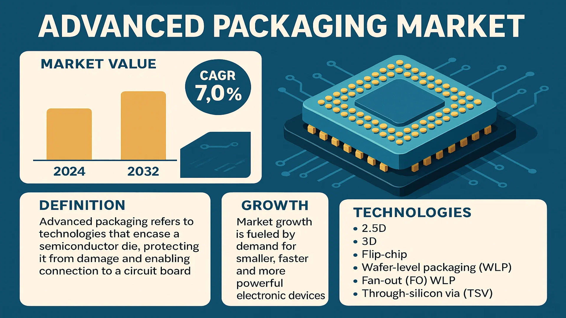
The global Advanced Packaging Market was valued at 14550 million in 2024 and is projected to reach US$ 23160 million by 2032, at a CAGR of 7.0% during the forecast period.
Advanced packaging refers to the suite of technologies and methodologies used to encase a semiconductor die, protecting it from physical damage and corrosion while enabling its connection to a circuit board. This process is a critical final step in semiconductor manufacturing, evolving significantly from the leadless chip carriers of the 1980s to modern, high-density solutions. These technologies include 2.5D, 3D, flip-chip, wafer-level packaging (WLP), fan-out (FO) WLP, and through-silicon via (TSV) configurations, which are essential for enhancing performance, reducing power consumption, and enabling the miniaturization of electronic devices.
The market is experiencing robust growth driven by the relentless demand for smaller, faster, and more powerful electronic devices across consumer electronics, automotive, and high-performance computing sectors. The proliferation of 5G, artificial intelligence (AI), and the Internet of Things (IoT) is a primary catalyst, as these technologies require sophisticated packaging solutions to manage heat and signal integrity. However, the industry faces challenges such as high manufacturing costs and complex thermal management requirements. Key players like ASE Group, Amkor Technology, and SPIL are leading the market with extensive portfolios and continuous innovation, ensuring the sector’s dynamic expansion.
MARKET DYNAMICS
MARKET DRIVERS
Proliferation of High-Performance Computing and AI Applications to Accelerate Market Expansion
The exponential growth in artificial intelligence, machine learning, and high-performance computing applications is fundamentally transforming the semiconductor packaging landscape. Advanced packaging technologies enable the integration of multiple heterogeneous chips into compact systems, delivering superior performance while reducing power consumption and latency. The demand for these solutions has surged dramatically, with AI chip revenue projected to exceed $100 billion annually by 2025. This growth is primarily driven by data centers, autonomous vehicles, and edge computing devices that require sophisticated packaging approaches like 2.5D and 3D integration. Major technology companies are increasingly adopting advanced packaging to overcome the limitations of traditional Moore’s Law scaling, creating sustained demand across multiple industry verticals.
Rising Adoption of 5G and IoT Devices to Fuel Market Growth
The global rollout of 5G networks and the proliferation of Internet of Things devices are creating unprecedented demand for advanced semiconductor packaging solutions. 5G technology requires sophisticated RF components and millimeter-wave chips that necessitate advanced packaging techniques for optimal performance. The IoT market, expected to connect over 30 billion devices by 2025, demands packaging solutions that offer miniaturization, low power consumption, and enhanced reliability. Advanced packaging technologies such as fan-out wafer-level packaging and system-in-package enable the integration of diverse functionalities—sensors, processors, and connectivity modules—into compact form factors essential for modern mobile devices and IoT endpoints. This convergence of connectivity and computing continues to drive innovation and investment in advanced packaging methodologies.
Automotive Electronics Revolution to Drive Packaging Innovation
The automotive industry’s transformation toward electrification, autonomy, and connectivity represents a significant growth driver for advanced packaging. Modern vehicles incorporate hundreds of semiconductor devices requiring robust packaging solutions that can withstand harsh environmental conditions while delivering high reliability. Advanced driver-assistance systems, electric vehicle power management, and in-vehicle infotainment systems all utilize sophisticated packaging technologies. The automotive semiconductor market has grown at approximately 8% annually, with advanced packaging becoming increasingly critical for meeting automotive-grade requirements. These applications demand packaging solutions that offer thermal management, high reliability, and miniaturization—factors that continue to push packaging technology boundaries and drive market expansion.
MARKET RESTRAINTS
High Capital Investment and Manufacturing Complexity to Constrain Market Penetration
Advanced packaging technologies require substantial capital investment in specialized equipment and cleanroom facilities, creating significant barriers to entry for many market participants. The transition from traditional packaging to advanced solutions involves capital expenditures that can exceed several hundred million dollars for a single production facility. This financial burden is particularly challenging for small and medium-sized enterprises seeking to compete in this market. Additionally, the manufacturing processes for technologies like 3D integration and through-silicon via require extreme precision and control, resulting in higher production costs compared to conventional packaging methods. These economic factors limit widespread adoption, especially in cost-sensitive applications and emerging markets where price competitiveness remains crucial.
Technical Challenges in Thermal Management and Signal Integrity to Hinder Market Development
As semiconductor devices become more densely packed in advanced packaging configurations, managing heat dissipation and maintaining signal integrity present significant technical challenges. The power density in 3D stacked chips can exceed 100 W/cm², creating thermal management issues that affect device reliability and performance. These challenges necessitate innovative cooling solutions and materials that increase overall system cost and complexity. Simultaneously, maintaining signal integrity at high data rates becomes increasingly difficult as interconnect densities rise and transmission distances decrease. These technical hurdles require extensive research and development efforts, slowing the adoption of advanced packaging in applications where reliability is paramount, such as automotive and aerospace electronics.
Supply Chain Vulnerabilities and Material Availability to Impact Market Stability
The advanced packaging industry faces ongoing challenges related to supply chain vulnerabilities and the availability of specialized materials. Many advanced packaging processes require unique substrates, adhesives, and thermal interface materials that have limited manufacturing sources globally. This concentration creates supply chain risks that became particularly evident during recent global disruptions, where lead times for certain packaging materials extended beyond six months. Additionally, the industry’s reliance on rare earth elements and specialized chemicals creates potential bottlenecks in production scalability. These supply chain constraints not only affect production timelines but also contribute to cost volatility, making long-term planning and pricing strategies challenging for both packaging providers and their customers.
MARKET CHALLENGES
Standardization and Interoperability Issues to Complicate Market Evolution
The advanced packaging industry faces significant challenges in establishing universal standards and ensuring interoperability between different packaging technologies and foundry processes. Unlike traditional packaging, which benefited from decades of standardization, advanced packaging encompasses numerous emerging technologies with proprietary implementations. This lack of standardization creates compatibility issues between chips from different manufacturers and increases integration complexity for system designers. The absence of widely accepted design rules, testing methodologies, and reliability standards forces companies to develop custom solutions, increasing development costs and time-to-market. These challenges are particularly acute in heterogeneous integration, where chips manufactured using different process technologies must work seamlessly together within a single package.
Other Challenges
Intellectual Property Protection and Technology Transfer Barriers
The highly competitive nature of advanced packaging has led to intense intellectual property protection measures that sometimes hinder technology sharing and collaboration. Companies invest heavily in proprietary packaging technologies and methodologies, creating legal and operational barriers to knowledge exchange. This environment complicates the development of industry-wide solutions and slows the pace of innovation diffusion. Additionally, export controls and technology transfer restrictions affect the global flow of advanced packaging expertise and equipment, particularly affecting emerging markets seeking to develop their packaging capabilities.
Testing and Quality Assurance Complexities
Advanced packaging introduces new testing challenges that traditional methods cannot adequately address. The complexity of 3D structures, hidden interconnects, and heterogeneous integration makes comprehensive testing difficult and expensive. Developing effective test strategies for known-good die and ensuring package-level reliability requires sophisticated equipment and methodologies that are still evolving. These testing challenges increase overall product development costs and create uncertainty regarding long-term reliability, particularly for safety-critical applications in automotive, medical, and aerospace industries.
MARKET OPPORTUNITIES
Emerging Applications in Healthcare and Medical Electronics to Create New Growth Avenues
The healthcare industry’s digital transformation is creating substantial opportunities for advanced packaging technologies. Medical devices, diagnostic equipment, and wearable health monitors increasingly require sophisticated packaging solutions that offer miniaturization, biocompatibility, and high reliability. The convergence of electronics and healthcare has accelerated, particularly with the growth of remote patient monitoring and implantable medical devices. Advanced packaging enables the development of smaller, more powerful medical electronics that can operate in challenging environments while meeting stringent regulatory requirements. This market segment represents a significant growth opportunity, with medical electronics expected to grow at approximately 7% annually, driven by aging populations and increasing healthcare technology adoption.
Advanced Packaging for Quantum Computing and Photonics to Enable Next-Generation Technologies
The emergence of quantum computing and integrated photonics represents a frontier opportunity for advanced packaging technologies. These cutting-edge applications require packaging solutions that can operate at cryogenic temperatures, manage exotic materials, and interface between electronic and photonic components. The quantum computing market, though still emerging, is projected to grow exponentially as technology matures and commercial applications develop. Similarly, silicon photonics adoption is increasing in data centers and high-performance computing applications, creating demand for packaging that can efficiently couple optical and electronic components. These emerging fields require fundamentally new packaging approaches, presenting opportunities for innovation and market leadership for companies that can develop the necessary expertise and capabilities.
Sustainable and Eco-Friendly Packaging Solutions to Address Environmental Concerns
Growing environmental awareness and regulatory pressure are driving demand for sustainable packaging solutions across the electronics industry. Advanced packaging technologies that reduce material usage, enable recycling, and eliminate hazardous substances represent a significant market opportunity. The industry is increasingly focusing on developing lead-free, halogen-free, and bio-based packaging materials that meet environmental standards without compromising performance. Additionally, packaging approaches that facilitate component reuse and recycling align with circular economy principles gaining traction worldwide. This sustainability focus creates opportunities for innovation in materials science and packaging architectures that minimize environmental impact while maintaining technical performance, particularly in consumer electronics and automotive applications where environmental regulations are most stringent.
ADVANCED PACKAGING MARKET TRENDS
Heterogeneous Integration and 3D Packaging Technologies Emerge as Dominant Trends
The relentless pursuit of miniaturization and enhanced performance in semiconductors is fundamentally reshaping the advanced packaging landscape, with heterogeneous integration (HI) and 3D packaging at the forefront. These technologies allow for the integration of multiple dies, fabricated using different process nodes and technologies, into a single package. This approach significantly improves system performance and energy efficiency while reducing the physical footprint, a critical factor for applications like artificial intelligence, high-performance computing, and 5G infrastructure. The market for 2.5D and 3D advanced packaging is experiencing substantial growth, driven by the insatiable demand for more powerful and compact electronic devices. While traditional scaling faces physical and economic limitations, advanced packaging offers a viable path forward, often described as ‘More than Moore.’ The integration of high-bandwidth memory (HBM) stacks with logic processors using through-silicon vias (TSVs) and microbumps is a prime example of this trend in action, enabling the massive data throughput required for modern computing tasks.
Other Trends
Proliferation of Fan-Out Wafer-Level Packaging (FOWLP)
Fan-Out Wafer-Level Packaging continues to gain significant traction due to its superior electrical performance, thinner profile, and cost-effectiveness at high I/O densities compared to older technologies like flip-chip ball grid array (FCBGA). This technology is increasingly being adopted for applications in mobile devices, networking, and automotive electronics. The ability to integrate multiple chips laterally on a reconstituted wafer provides design flexibility and reduces the overall package size. The FOWLP market segment is projected to be one of the fastest-growing, as it effectively bridges the gap between traditional packaging and more complex 2.5D/3D solutions. Its adoption is particularly strong in radio frequency and power management applications, where performance and form factor are paramount.
Surging Demand from Artificial Intelligence and Machine Learning Workloads
The explosive growth of artificial intelligence (AI) and machine learning (ML) is acting as a primary catalyst for innovation and investment in the advanced packaging sector. AI accelerators, GPUs, and specialized ASICs require immense memory bandwidth and low-latency communication between logic and memory dies, demands that can only be met by advanced packaging techniques like 2.5D interposers and 3D stacking. The data center segment, in particular, is a major consumer of these high-performance packaging solutions. The need to process vast datasets efficiently is pushing chip designers toward architectures that rely on advanced packaging to overcome the bottlenecks associated with traditional off-chip connections. This trend is not only driving volume but also spurring R&D into new materials, thermal management solutions, and testing methodologies to handle the increased power densities and structural complexities inherent in these advanced packages.
Increased Focus on Supply Chain Resilience and Geographic Diversification
Recent global disruptions have underscored the critical importance of a resilient semiconductor supply chain, prompting significant strategic shifts within the advanced packaging industry. Governments and major corporations are actively investing in packaging and testing facilities outside of traditional hubs to mitigate geopolitical risks and ensure a more stable supply of packaged chips. This has led to a notable increase in capital expenditure for new advanced packaging facilities in regions like the United States, Europe, and Southeast Asia. This trend towards geographic diversification is reshaping the competitive landscape and fostering new collaborations between foundries, integrated device manufacturers (IDMs), and outsourced semiconductor assembly and test (OSAT) companies. The goal is to build a more robust and geographically distributed infrastructure capable of supporting the next generation of electronic products without being vulnerable to single points of failure.
COMPETITIVE LANDSCAPE
Key Industry Players
Technological Innovation and Strategic Expansion Drive Market Leadership
The global advanced packaging market is characterized by a semi-consolidated structure, featuring a mix of large-scale international corporations and specialized regional players. This dynamic is driven by the critical need for sophisticated packaging solutions that support the miniaturization and performance demands of modern semiconductors across applications like artificial intelligence, high-performance computing, and 5G connectivity.
ASE Technology Holding Co., Ltd. (Taiwan) is a dominant force, holding a significant revenue share estimated at over 20% in 2024. Its leadership is anchored in a comprehensive portfolio that includes fan-out wafer-level packaging (FO WLP) and 2.5D/3D IC integration services. The company’s extensive manufacturing footprint across Taiwan, China, and Malaysia, coupled with consistent R&D investment, allows it to serve a global clientele and maintain a competitive edge.
Similarly, Amkor Technology, Inc. (USA) and JCET Group (China) are pivotal players, each commanding a substantial portion of the market. Amkor’s strength lies in its advanced flip-chip and system-in-package (SiP) technologies, particularly for automotive and communication applications. JCET has rapidly ascended through strategic acquisitions and a strong focus on expanding its FO WLP and bumping capabilities, solidifying its position as a top-tier provider.
These leading companies are aggressively pursuing growth through capacity expansion and technological partnerships. For instance, significant investments are being channeled into new fabrication plants and the development of cutting-edge solutions for heterogeneous integration. This focus on innovation is crucial because it directly addresses the industry’s shift towards more complex, multi-die packages that offer higher performance in smaller form factors.
Meanwhile, other key participants like SPIL (Taiwan) and Stats Chippac (Singapore) are strengthening their market positions through specialized expertise and targeted expansions. Their strategies often involve deepening capabilities in specific high-growth segments, such as MEMS and sensor packaging for IoT devices or advanced packaging for RF applications, ensuring their relevance in an evolving competitive landscape.
List of Key Advanced Packaging Companies Profiled
- ASE Technology Holding Co., Ltd. (Taiwan)
- Amkor Technology, Inc. (U.S.)
- Siliconware Precision Industries Co., Ltd. (SPIL) (Taiwan)
- Stats Chippac Pte. Ltd. (Singapore)
- Powertech Technology Inc. (PTI) (Taiwan)
- JCET Group (China)
- J-Devices Corporation (Japan)
- United Test and Assembly Center Ltd. (UTAC) (Singapore)
- ChipMOS TECHNOLOGIES INC. (Taiwan)
- Chipbond Technology Corporation (Taiwan)
- STS Semiconductor & Telecommunications Co., Ltd. (South Korea)
- Tianshui Huatian Technology Co., Ltd. (China)
- NFM (China)
- Carsem (Malaysia)
- Walton Advanced Engineering Inc. (Taiwan)
- Unisem (M) Berhad (Malaysia)
- OSE Co., Ltd. (South Korea)
- AOI Electronics Co., Ltd. (Japan)
- Formosa Advanced Technologies Co., Ltd. (Taiwan)
- NEPES (South Korea)
Segment Analysis:
By Type
Flip Chip Segment Dominates the Market Due to Superior Electrical Performance and High-Density Interconnects
The market is segmented based on type into:
- Flip Chip
- Fan-Out Wafer Level Packaging (FO WLP)
- 2.5D
- 3D Integrated Circuit (3D IC)
- Wafer-Level Chip Scale Packaging (WLCSP)
- Others
By Application
MEMS & Sensor Segment Leads Due to Pervasive Use in Consumer Electronics and Automotive Systems
The market is segmented based on application into:
- MEMS & Sensor
- Wireless Connectivity
- Analog & Mixed Signal
- Optoelectronic
- Misc Logic and Memory
- Other
By End-User Industry
Consumer Electronics Segment Holds the Largest Share Driven by Smartphones and Wearables
The market is segmented based on end-user industry into:
- Consumer Electronics
- Automotive
- Telecommunications
- Industrial
- Healthcare
- Others
Regional Analysis: Advanced Packaging Market
Asia-Pacific
The Asia-Pacific region is the undisputed global leader in the advanced packaging market, accounting for over 60% of worldwide revenue. This dominance is driven by the massive semiconductor manufacturing ecosystems in Taiwan, South Korea, and China. Taiwan, home to industry titans like ASE and SPIL, is a powerhouse in Outsourced Semiconductor Assembly and Test (OSAT) services. The region’s growth is fueled by insatiable demand for consumer electronics, automotive semiconductors, and high-performance computing chips. While China is aggressively expanding its domestic capabilities through significant national investments, mature markets like Taiwan and South Korea continue to lead in innovation, particularly in cutting-edge technologies like 2.5D/3D integration and fan-out wafer-level packaging (FOWLP) to support next-generation AI and data center applications.
North America
North America, particularly the United States, is a key innovation hub for advanced packaging technologies, driven by leading fabless semiconductor companies and integrated device manufacturers (IDMs). The region’s market is characterized by a strong focus on research and development, with significant investments in heterogeneous integration and chiplets architecture to overcome the limitations of Moore’s Law. The CHIPS and Science Act, which allocates billions in funding for domestic semiconductor research and production, is a major catalyst, explicitly supporting advancements in packaging. This environment fosters collaboration between companies like Amkor, which has major operations in the U.S., and tech giants requiring advanced packaging for their most sophisticated processors. The demand is primarily driven by high-performance computing, artificial intelligence, and aerospace and defense applications.
Europe
Europe’s advanced packaging market is strategically focused on high-value applications, particularly in the automotive, industrial, and healthcare sectors. The region boasts strong capabilities in power electronics and MEMS & sensor packaging, which are critical for the automotive industry’s shift toward electrification and autonomy. Strict environmental regulations, such as the EU’s RoHS directive, push innovation toward more sustainable packaging materials and processes. While the region’s OSAT presence is smaller compared to Asia, it is supported by a robust network of research institutions and a strong emphasis on quality and reliability. Recent initiatives like the European Chips Act aim to bolster the entire semiconductor value chain, including packaging, to reduce strategic dependencies and secure supply for its key manufacturing industries.
South America
The advanced packaging market in South America is nascent and primarily serves local consumer electronics and industrial manufacturing demands. The region lacks a significant semiconductor fabrication base, making it heavily reliant on imported packaged chips. Countries like Brazil have some assembly and test operations, but the market is constrained by economic volatility, limited investment in high-tech infrastructure, and a smaller local demand for leading-edge technology. Growth is steady but slow, driven by basic consumer electronics assembly and the automotive sector. The potential for future development exists, but it hinges on greater economic stability and targeted government policies to attract investment into the electronics manufacturing value chain.
Middle East & Africa
This region represents an emerging and opportunistic market for advanced packaging. While currently holding a very small share of the global market, certain nations, particularly in the Middle East, are making strategic investments to diversify their economies beyond oil and gas. Initiatives like Saudi Arabia’s Vision 2030 include developing a technology sector, which could eventually incorporate semiconductor packaging. The current market demand is almost entirely met through imports, serving telecommunications infrastructure and consumer goods. Long-term growth potential is tied to economic diversification plans, but the market faces significant challenges, including a lack of existing semiconductor infrastructure, expertise, and a need for substantial, sustained investment.
Report Scope
This market research report provides a comprehensive analysis of the global and regional Advanced Packaging markets, covering the forecast period 2025–2032. It offers detailed insights into market dynamics, technological advancements, competitive landscape, and key trends shaping the industry.
Key focus areas of the report include:
- Market Size & Forecast: Historical data and future projections for revenue, unit shipments, and market value across major regions and segments.
- Segmentation Analysis: Detailed breakdown by product type, technology, application, and end-user industry to identify high-growth segments and investment opportunities.
- Regional Outlook: Insights into market performance across North America, Europe, Asia-Pacific, Latin America, and the Middle East & Africa, including country-level analysis where relevant.
- Competitive Landscape: Profiles of leading market participants, including their product offerings, R&D focus, manufacturing capacity, pricing strategies, and recent developments such as mergers, acquisitions, and partnerships.
- Technology Trends & Innovation: Assessment of emerging technologies, integration of AI/IoT, semiconductor design trends, fabrication techniques, and evolving industry standards.
- Market Drivers & Restraints: Evaluation of factors driving market growth along with challenges, supply chain constraints, regulatory issues, and market-entry barriers.
- Stakeholder Analysis: Insights for component suppliers, OEMs, system integrators, investors, and policymakers regarding the evolving ecosystem and strategic opportunities.
Primary and secondary research methods are employed, including interviews with industry experts, data from verified sources, and real-time market intelligence to ensure the accuracy and reliability of the insights presented.
FREQUENTLY ASKED QUESTIONS:
What is the current market size of Global Advanced Packaging Market?
-> Advanced Packaging Market was valued at 14550 million in 2024 and is projected to reach US$ 23160 million by 2032, at a CAGR of 7.0% during the forecast period.
Which key companies operate in Global Advanced Packaging Market?
-> Key players include ASE, Amkor, SPIL, Stats Chippac, PTI, JCET, J-Devices, UTAC, Chipmos, Chipbond, STS, Huatian, NFM, Carsem, Walton, Unisem, OSE, AOI, Formosa, and NEPES, among others.
What are the key growth drivers?
-> Key growth drivers include rising demand for high-performance computing, miniaturization of electronic devices, growth in 5G infrastructure, and increasing adoption of IoT and AI technologies.
Which region dominates the market?
-> Asia-Pacific dominates the market, accounting for over 65% of global revenue in 2024, driven by strong semiconductor manufacturing presence in Taiwan, South Korea, and China.
What are the emerging trends?
-> Emerging trends include heterogeneous integration, 3D packaging technologies, fan-out wafer-level packaging (FOWLP), and the development of advanced materials for thermal management.

Get Sample Report PDF for Exclusive Insights
Report Sample Includes
- Table of Contents
- List of Tables & Figures
- Charts, Research Methodology, and more...


