Key Statistics
Key Takeaways
- ArF immersion holds the largest revenue share in 2025 while EUV is the fastest-growing type. ASML’s fourth-quarter bookings split EUR 7.4 billion EUV against EUR 5.8 billion non-EUV, an early indicator of where the mix is heading even though immersion still carries the larger installed base.
- Front-end wafer processing dominates the market, but advanced packaging is the fastest-growing application as chiplet integration and 2.5D and 3D stacking push lithographic patterning into steps that previously required no exposure tool at all.
- Asia-Pacific is the largest and fastest-growing region. SEMI reported that China, Taiwan and Korea took 79% of global semiconductor equipment billings in 2025, up from 74% a year earlier, with Taiwan surging 90% to a record USD 31.5 billion.
- Market concentration is the highest of any semiconductor equipment category. ASML reported 2025 net sales of EUR 32.7 billion with net income of EUR 9.6 billion at a 52.8% gross margin, and is the sole supplier of EUV systems worldwide – a position no other equipment segment approaches.
- Backlog gives unusual forward visibility. ASML closed 2025 with a EUR 38.8 billion backlog after net bookings of EUR 28.035 billion, and guided 2026 net sales to EUR 34–39 billion, so near-term demand is largely contracted rather than forecast.
- Export control is a structural feature of this market, not a passing risk. Since 7 September 2024 the Netherlands has required authorisation for exports of advanced semiconductor manufacturing equipment, including deep ultraviolet lithography systems, to destinations outside the EU, assessed case by case.
Semiconductor Photolithography Equipment Market Overview
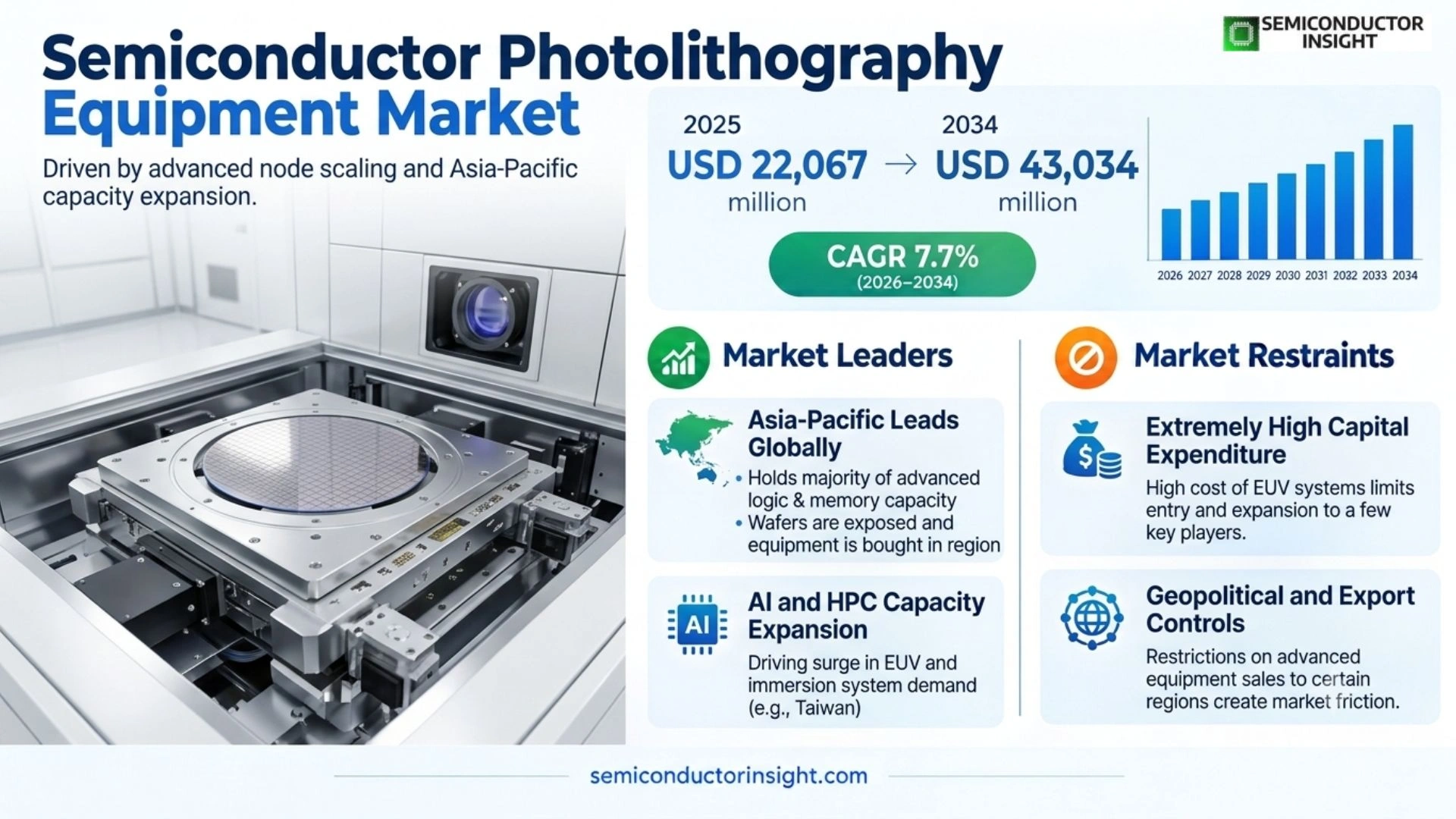
Semiconductor Photolithography Equipment Market was valued at USD 22,067 million in 2025 and is projected to reach USD 43,034 million by 2034, expanding at a CAGR of 7.7% across the 2026–2034 forecast period. Asia-Pacific held the largest regional share in 2025 and is also the fastest-growing region, mirroring the concentration of advanced logic and memory capacity across Taiwan, South Korea, China and Japan.
Photolithography equipment projects a circuit pattern from a photomask onto a light-sensitive resist coating on a wafer, defining every feature that will subsequently be etched, implanted or deposited. It is the step that sets the minimum feature size a fab can produce, and therefore the step that determines which process node a facility can run at all. No other tool in the fab has that gating relationship to capability rather than merely to throughput.
The category divides by exposure wavelength, and each generation exists because the one before it reached a physical resolution limit. I-line and KrF systems pattern mature-node and non-critical layers. ArF dry and ArF immersion systems, the latter using water between lens and wafer to raise numerical aperture, carry the bulk of critical-layer work at established nodes. Extreme ultraviolet at 13.5 nm enables the leading edge, at a cost and complexity discontinuity unlike any previous transition.
Scope covers wafer exposure systems across the full wavelength range – EUV, ArF immersion, ArF dry, KrF and i-line – together with the mask aligners, steppers and direct-write systems used in back-end and advanced packaging applications, and the installed base service, upgrade and field option revenue that accompanies them. Photomasks, resist chemistry, track and coater-developer systems, metrology and inspection equipment sit outside the definition.
The market’s scale and concentration are both exceptional. ASML reported 2025 total net sales of EUR 32.7 billion with net income of EUR 9.6 billion at a 52.8% gross margin, sold 300 new lithography systems during the year, and generated EUR 8.193 billion from installed base management alone. It is the sole supplier of EUV systems worldwide, a monopoly position no other semiconductor equipment category contains.
Demand visibility is correspondingly unusual. ASML closed 2025 with a backlog of EUR 38.8 billion following net bookings of EUR 28.035 billion, including EUR 13.2 billion in the fourth quarter alone – EUR 7.4 billion of it EUV and EUR 5.8 billion non-EUV – and guided 2026 net sales to EUR 34–39 billion at a 51–53% gross margin. Near-term revenue in this category is largely contracted rather than forecast.
The wider equipment cycle supports that outlook. Global semiconductor equipment billings reached USD 135.1 billion in 2025, up 15%, and SEMI projects 300 mm fab equipment spending of USD 133 billion in 2026, rising to USD 151 billion in 2027 and USD 172 billion in 2029, with cumulative 2027–2029 spending of USD 374 billion split USD 228 billion to logic and micro and USD 175 billion to memory – the two segments that consume advanced lithography.
Segment Analysis: By Type
By exposure source, the market is segmented into EUV, ArF immersion, ArF dry, KrF and i-line systems. ArF immersion holds the largest revenue share in 2025 on the strength of its installed base and its role across critical layers at established nodes, while EUV is the fastest-growing type and the source of most incremental value in the category.
| Type | Function | Market position |
|---|---|---|
| EUV Lithography | Exposes at 13.5 nm using tin-plasma-generated extreme ultraviolet light in a fully reflective, vacuum optical path, with High-NA variants extending resolution further | Fastest-growing type and the highest value per unit in the industry. Supplied solely by ASML, whose fourth-quarter 2025 bookings included EUR 7.4 billion of EUV against EUR 5.8 billion non-EUV. EUV replaces the multi-patterning sequences that would otherwise be needed at leading-edge nodes, trading enormous tool cost and complexity for a reduction in process steps, cycle time and cumulative overlay error. Adoption is limited to manufacturers with the scale to absorb both the capital and the infrastructure it requires. |
| ArF Immersion (ArFi) | Exposes at 193 nm with purified water between the final lens element and the wafer, raising numerical aperture and therefore resolution | Largest revenue share in 2025. The workhorse of critical-layer patterning and the most widely installed advanced platform in the industry. It remains essential even in EUV-equipped fabs, since not every critical layer justifies EUV exposure, and multi-patterning on immersion tools continues to serve nodes where EUV is unavailable or uneconomic. Its installed base also generates the largest share of service and upgrade revenue. |
| ArF Dry | Exposes at 193 nm without an immersion medium, serving critical layers at established nodes and non-critical layers at advanced ones | A mature segment with steady demand, positioned between KrF and immersion in both capability and cost. Its enduring role is in mature-node logic, analogue and power device manufacture where immersion resolution is unnecessary and its cost unjustified. Demand tracks mature-node capacity additions, which have been substantial in China and in automotive-oriented capacity elsewhere. |
| KrF Lithography | Exposes at 248 nm, patterning mid-range geometries across mature logic, memory periphery and a wide range of specialty devices | A large, stable installed base serving mature-node manufacturing, discrete and power devices, and non-critical layers throughout advanced flows. Demand is driven by mature-node capacity expansion rather than by technology transition, and the segment has a materially broader supplier base than the advanced tiers – the principal reason competitive dynamics differ so sharply between the two ends of this market. |
| I-line Lithography | Exposes at 365 nm using mercury lamp illumination, patterning coarse geometries in mature devices and back-end packaging applications | The most mature exposure technology and the most price-competitive segment. Its position is secure but not growing through node progression; instead it is finding renewed demand in advanced packaging, where redistribution layers, bumping and interposer patterning need reliable coarse-geometry exposure rather than leading-edge resolution – the one place where an older technology is gaining a genuinely new application. |
Why the two ends of this market behave like separate industries
Advanced lithography and mature lithography share a physical principle and almost nothing else commercially. At the leading edge, a single supplier sells systems priced in the tens of millions to a handful of manufacturers, under export control, with multi-year lead times and contracted backlog. At mature nodes, several suppliers compete for orders from a wide customer base on price, delivery and service. Treating these as one market obscures more than it explains.
Value beyond the exposure tool itself
Installed base management is a substantial and stable revenue stream that pure system sales figures conceal. ASML generated EUR 8.193 billion from installed base management in 2025 – roughly a quarter of total net sales – through service contracts, field upgrades, performance options and refurbishment. Because lithography systems remain in production for a decade or more and are progressively upgraded rather than replaced, this revenue compounds with the installed base rather than cycling with new orders.
Segment Analysis: By Application
By application, the market divides into front-end wafer processing, back-end assembly and test, and advanced packaging, and by end user across logic chip manufacturers, memory chip manufacturers and advanced packaging service providers. Front-end processing dominates revenue because exposure determines the node a fab can run, while advanced packaging is the fastest-growing application as chiplet integration and stacking push patterning into steps that previously required no exposure tool.
| Application | Demand characteristics |
|---|---|
| Front-end Process | The dominant application by revenue. Wafer-level patterning of transistors and interconnect across logic and memory, where lithography sets the achievable node. SEMI’s projected cumulative 2027–2029 300 mm equipment spending of USD 374 billion – USD 228 billion for logic and micro and USD 175 billion for memory – flows predominantly here. Exposure tool selection determines a fab’s capability rather than merely its output, which is why lithography procurement decisions are made at corporate rather than site level. |
| Advanced Packaging | Fastest-growing application. Chiplet integration, 2.5D interposers, 3D stacking, redistribution layers, through-silicon via patterning and fan-out wafer-level packaging. Growth is structural: as monolithic scaling slows, performance gains increasingly come from integration, and integration requires patterning steps that packaging operations previously did not perform. SEMI recorded assembly and packaging equipment billings up 21% in 2025. Resolution requirements are modest by front-end standards, which is why i-line and KrF systems find new demand here. |
| Back-end Process | Bumping, wafer-level chip-scale packaging and other post-fabrication patterning performed at assembly and test facilities. Requirements emphasise throughput, overlay on warped substrates and cost per exposure rather than resolution. Suppliers competing here – including those serving mask aligner and stepper applications – face a customer base with fundamentally different economics from front-end fabs, buying against cost per package rather than against node capability. |
| Logic and memory end users | Logic manufacturers drive EUV and immersion demand at the leading edge and set the pace of technology adoption, while memory manufacturers are the larger consumers of repeated patterning at established nodes and are increasingly adopting EUV for advanced DRAM. SEMI’s split of USD 228 billion logic and micro against USD 175 billion memory across 2027–2029 describes how the two segments divide the forward equipment programme. |
Regional Analysis
Asia-Pacific is the largest regional market for semiconductor photolithography equipment in 2025 and also the fastest-growing. SEMI reported that China, Taiwan and Korea together took 79% of global semiconductor equipment billings in 2025, up from 74% in 2024, with Taiwan surging 90% to a record USD 31.5 billion, Korea rising 26% to USD 25.8 billion and Japan 22% to USD 9.5 billion.
How does regional demand differ across the photolithography equipment market?
Regional shares in lithography restate where advanced capacity is being equipped, but they are also shaped by export control in a way no other equipment category matches. Taiwan and Korea buy leading-edge systems without restriction; China buys mature and mid-range systems under a licensing regime that governs what may be supplied at all; North America and Europe are building capacity but sit mid-cycle between construction and equipping. Policy is a demand variable here, not a background condition.
| Region | Position | Growth outlook | Demand profile | What decides supplier selection |
|---|---|---|---|---|
| Asia-Pacific | Largest | Highest in market | Advanced capacity led | Node capability, delivery slot availability, export licensing, service density |
| North America | Second largest | High | Greenfield project led | Leading-edge capability, delivery timing against construction schedule, domestic service capacity |
| Europe | Third largest | Moderate | Specialty and supply-side led | Mature-node capability, configurability, proximity to the supplier engineering base |
| South America | Smallest | Emerging | Research and packaging led | Delivered cost, support access, refurbished system availability |
| Middle East & Africa | Smallest base | Emerging | Project led | Project delivery, service establishment, technology access |
Key Photolithography Equipment Manufacturers and Competitive Landscape
This is the most concentrated segment in semiconductor equipment. ASML is the sole supplier of EUV systems worldwide and reported 2025 net sales of EUR 32.7 billion with net income of EUR 9.6 billion at a 52.8% gross margin. Nikon and Canon compete in ArF and KrF and in specialised approaches, SMEE develops domestic Chinese capability, and EV Group, SUSS MicroTec and Veeco’s Ultratech business serve packaging and mask alignment.
The barrier protecting the leading position is not patents or capital but supply-chain orchestration accumulated over decades. An EUV system integrates a tin-plasma light source, multilayer reflective optics polished to atomic tolerances, vacuum handling and control systems drawing on thousands of specialist suppliers. Reproducing that network is a multi-decade industrial undertaking rather than an engineering project, which is why the monopoly has persisted through sustained commercial and political pressure to end it.
Competition at mature nodes is genuinely different and considerably healthier. Nikon and Canon hold real positions in KrF, i-line and ArF systems, where the customer base is broad, resolution requirements are settled and purchasing turns on price, delivery and service rather than on unique capability. Canon has also pursued nanoimprint lithography as an alternative patterning route, an approach that sidesteps the optical scaling problem rather than competing within it.
A third competitive layer serves packaging and back-end patterning, and it is growing fastest. EV Group, SUSS MicroTec and Veeco’s Ultratech business supply mask aligners, steppers and bonding-adjacent systems into advanced packaging operations, where SEMI recorded assembly and packaging equipment billings up 21% in 2025. Resolution requirements here are modest, the customer base is wide, and competition resembles a normal capital equipment market.
Domestic capability development under industrial policy is the fourth dynamic and the most closely watched. SMEE develops lithography systems within China, supported by localisation policy and by a domestic market that took USD 49.3 billion of equipment billings in 2025. Progress at mature nodes is commercially meaningful in its own right, independently of whether advanced capability follows, because mature-node exposure is a large and durable segment.
Tier structure
| Tier | Companies | Basis of competition |
|---|---|---|
| Tier 1 – Advanced exposure | ASML | Sole global supplier of EUV systems and leading supplier of ArF immersion; competitive position rests on decades of supply-chain orchestration, installed base service and contracted backlog |
| Tier 2 – Established alternatives | Nikon, Canon | Real positions in ArF, KrF and i-line systems where the customer base is broad and purchasing turns on price, delivery and service; Canon additionally pursues nanoimprint lithography as an alternative patterning route |
| Tier 3 – Packaging, mask alignment and emerging domestic capability | EV Group, SUSS MicroTec, Ultratech (Veeco Instruments), SMEE | Advanced packaging and back-end patterning, mask alignment and bonding-adjacent systems, and domestic capability development supported by national industrial policy |
Several organisations named in the report scope participate in this market indirectly rather than as exposure system suppliers, and it is worth stating the distinction plainly. Tokyo Electron and Lam Research supply adjacent process steps including coater-developer tracks and etch; DNP supplies photomasks; Rudolph Technologies serves inspection and process control; and Intel and Samsung operate internal lithography research programmes as customers advancing patterning capability rather than as equipment vendors.
Key companies profiled
- ASML
- Nikon
- Canon
- SMEE
- Tokyo Electron
- Ultratech (Veeco Instruments)
- EV Group
- SUSS MicroTech
- Rudolph Technologies
- DNP
- Lam Research
- NTT
- Accuray
- Intel (lithography R&D unit)
- Samsung (internal lithography development)
Photolithography Equipment Production Capacity Analysis
Production is concentrated in the Netherlands and Japan, at annual volumes measured in hundreds of systems rather than thousands. ASML sold 300 new lithography systems in 2025. Output is constrained not by assembly floor space but by a supply chain of specialist optics, light source and precision mechanics vendors whose capacity expands slowly and cannot be substituted.
An advanced exposure system is among the most complex machines manufactured anywhere. It integrates a light source, reflective or refractive optics held to sub-nanometre tolerances, vacuum systems, wafer and reticle stages positioned to atomic precision, and control software coordinating all of it at production throughput. Final assembly is performed in cleanroom conditions and followed by extended qualification before shipment, with installation and calibration at the customer site taking months more.
Volume tells the story better than revenue does. ASML sold 300 new lithography systems in 2025 alongside used system sales, delivering 94 new and 8 used systems in the fourth quarter alone, against total net sales of EUR 32.7 billion. A production rate in the hundreds means every unit is effectively built to order, and it explains why backlog rather than inventory is the operative planning variable across the industry.
The binding constraint sits upstream in a specialist supplier network. Precision optics, light source subsystems, high-precision stages and metrology components come from a small number of vendors whose own capacity expansion requires years of investment and skilled labour that is scarce. Because these components cannot be second-sourced in any practical sense, the industry’s output ceiling is set by the slowest-expanding link rather than by the system integrator’s own capacity.
Backlog is therefore the industry’s real capacity signal. ASML closed 2025 with EUR 38.8 billion of backlog after net bookings of EUR 28.035 billion, and guided 2026 net sales to EUR 34–39 billion. When demand exceeds the ability to build, delivery slot allocation becomes a strategic matter for customers – determining not merely when a fab receives a tool but when it can begin producing at a given node.
Photolithography Equipment Market Dynamics: Drivers, Restraints and Opportunities
Growth is driven by AI-led advanced logic and memory capacity expansion, by EUV adoption extending into DRAM, by advanced packaging creating new lithographic demand, and by installed base service revenue that compounds with the deployed fleet. The principal restraints are export control, supply chain capacity limits on system output, and the capital intensity that restricts advanced adoption to a handful of manufacturers.
MARKET DRIVERS
Drivers Impact Analysis*
| Driver | (~) % impact on CAGR forecast | Geographic relevance | Impact timeline |
|---|---|---|---|
| AI-driven advanced logic and memory capacity expansion | +2.8% | Taiwan, South Korea, United States, Japan | Short term (≤ 2 years) |
| EUV adoption extending from leading-edge logic into advanced DRAM | +1.9% | South Korea, Taiwan, United States | Medium term (2–4 years) |
| Advanced packaging creating lithographic demand where none existed | +1.4% | Taiwan, South Korea, United States, Southeast Asia | Medium term (2–4 years) |
| Installed base service, upgrade and field option revenue | +0.9% | Global, mature fab regions first | Long term (≥ 4 years) |
| Mature-node capacity expansion for automotive and industrial devices | +0.6% | China, Europe, Japan | Medium term (2–4 years) |
| Government-funded regional capacity programmes | +0.4% | United States, Europe, Japan, India | Long term (≥ 4 years) |
AI capacity expansion is the immediate driver
Taiwan’s semiconductor equipment billings rose 90% to a record USD 31.5 billion in 2025, which SEMI attributed to AI- and HPC-driven capacity expansion, while global billings reached USD 135.1 billion, up 15%. Because leading-edge logic consumes the most advanced and most expensive exposure systems, this spending translates into lithography demand at higher value intensity than into any other equipment category – visible in ASML’s EUR 13.2 billion of fourth-quarter bookings.
EUV is extending beyond leading-edge logic
EUV adoption began in advanced logic and is now moving into advanced DRAM, where critical layers increasingly justify the cost. Korea’s 26% billings increase to USD 25.8 billion in 2025 reflects that memory investment. Extending EUV into memory materially widens the addressable customer set for the highest-value systems in the industry, and it is the most important structural development in the category’s demand mix.
Advanced packaging creates patterning demand where none existed
As monolithic scaling slows, performance gains increasingly come from integration – chiplets, interposers, 3D stacking and redistribution layers – and each requires lithographic patterning at steps that packaging operations previously performed without any exposure tool. SEMI recorded assembly and packaging equipment billings up 21% in 2025. This is genuinely additive demand, and notably it accrues to i-line and KrF systems rather than to the advanced tiers.
MARKET RESTRAINTS
Restraints Impact Analysis*
| Restraint | (~) % impact on CAGR forecast | Geographic relevance | Impact timeline |
|---|---|---|---|
| Export control restricting advanced system sales to certain markets | -1.6% | China principally; supplier revenue globally | Medium term (2–4 years) |
| Supply chain capacity limiting annual system output | -1.2% | Global | Medium term (2–4 years) |
| Capital intensity restricting advanced adoption to few manufacturers | -0.9% | Global, second-tier manufacturers most | Long term (≥ 4 years) |
| Customer concentration exposing suppliers to few purchasing decisions | -0.7% | Global | Medium term (2–4 years) |
| Cyclicality of memory-driven capital spending | -0.5% | South Korea, Japan, United States | Short term (≤ 2 years) |
Export control is a permanent operating condition
Since 7 September 2024 the Netherlands has required authorisation for exports of advanced semiconductor manufacturing equipment, including deep ultraviolet lithography systems, to destinations outside the EU, with applications assessed individually. The Dutch government cited increased security risks in the current geopolitical context and the country’s unique leading position in the sector. For a supplier whose largest single regional market took USD 49.3 billion of equipment billings in 2025, licensing is a first-order commercial variable.
The industry cannot build systems faster than its suppliers allow
ASML sold 300 new lithography systems in 2025 and closed the year with a EUR 38.8 billion backlog. Output is limited by specialist optics, light source and precision mechanics suppliers whose capacity expands over years and cannot be second-sourced. This caps how quickly demand converts to revenue, and it means that in strong cycles the constraint on this market is manufacturing capability rather than customer appetite.
Capital intensity narrows the customer base
An advanced exposure system costs tens of millions of dollars and requires supporting infrastructure, trained personnel and sufficient wafer volume to amortise. Only manufacturers operating at very large scale can justify EUV adoption, which concentrates the highest-value demand among a handful of companies. That concentration is commercially attractive when they are investing and correspondingly exposed when any one of them pauses.
MARKET OPPORTUNITIES
High-NA EUV as the next capability step
High numerical aperture EUV extends resolution beyond current systems and is the defined path for nodes below present leading-edge geometries. For the supplier it commands the highest system prices in the industry and renews the upgrade cycle among existing EUV customers; for manufacturers it determines who can access the next node at all, which makes early adoption a competitive question rather than a procurement one.
Advanced packaging lithography as a broad-based growth segment
Packaging patterning uses coarse geometries, serves a wide customer base including OSATs and packaging service providers, and competes on throughput and cost per exposure rather than on resolution. SEMI recorded assembly and packaging equipment billings up 21% in 2025. This segment offers volume growth and a normal competitive structure – genuine opportunity for suppliers who cannot compete at the leading edge.
Installed base service and upgrade revenue
ASML generated EUR 8.193 billion from installed base management in 2025, roughly a quarter of total net sales, through service contracts, field upgrades and performance options. Because systems remain productive for a decade or more and are progressively upgraded rather than replaced, this revenue compounds with the installed fleet and is materially less cyclical than system sales – the most attractive structural characteristic in the category.
Mature-node and regional capability programmes
Government-funded capacity programmes across the United States, Europe, Japan and India, together with sustained mature-node investment for automotive and industrial devices, create demand for KrF, i-line and ArF dry systems from a widening set of customers. Competition in these segments is normal rather than monopolistic, which makes them the realistic growth ground for Nikon, Canon, SMEE and packaging-focused suppliers.
Photolithography Equipment Supply Chain Analysis
The value chain runs from precision optics, light sources and ultra-precision mechanics through system integration and qualification to direct supply into a small number of semiconductor manufacturers. Value concentrates upstream in irreplaceable component suppliers and downstream in installed base service, while system integration in the middle carries the industry’s defining orchestration challenge.
Upstream. This is where the industry’s true bottleneck lives. Precision optics polished to atomic tolerances, plasma and excimer light sources, and ultra-precision stages come from a very small group of specialists whose capacity expands over years and whose output cannot be second-sourced in any practical sense. The system integrator’s production rate is set by the slowest-expanding of these suppliers, which is why capacity increases in this market are announced years ahead.
Manufacturing. Integration is performed in cleanroom conditions and concludes with extended qualification testing before a system is disassembled for shipment and rebuilt at the customer site. Installation and calibration take months, during which the supplier’s engineers are effectively embedded in the customer’s fab. That process is itself a competitive asset: the knowledge accumulated across hundreds of installations cannot be acquired by a new entrant at any price.
Channel. Supply is direct, under multi-year agreements, to a customer base small enough to name – and it is subject to export licensing that determines which customers may be served at all. The combination of contracted backlog, allocation of delivery slots and regulatory authorisation makes this channel unlike any other in capital equipment: the purchase decision is only one of several gates a transaction must pass.
Downstream. A lithography system remains productive for a decade or more and is progressively upgraded with field options and performance enhancements rather than replaced, generating the installed base revenue that reached EUR 8.193 billion for ASML in 2025. Customer relationships are therefore continuous rather than transactional, and the supplier’s engineers remain present in the fab throughout the system’s operating life.
Recent Developments in the Photolithography Equipment Market
- 7 April 2026 Market data
SEMI reported global semiconductor equipment billings of USD 135.1 billion in 2025, up 15% from USD 117.1 billion in 2024. Taiwan surged 90% to a record USD 31.5 billion on AI- and HPC-driven capacity expansion, Korea rose 26% to USD 25.8 billion and Japan 22% to USD 9.5 billion, while China held roughly flat at USD 49.3 billion, North America fell 20% to USD 10.9 billion and Europe fell 41% to USD 2.9 billion. China, Taiwan and Korea together took 79% of global billings, up from 74% in 2024. Assembly and packaging equipment billings rose 21%.
Source - 1 April 2026 Market data
SEMI projected 300 mm fab equipment spending of USD 133 billion in 2026, an 18% increase, rising to USD 151 billion in 2027, USD 155 billion in 2028 and USD 172 billion in 2029. Cumulative 2027–2029 spending of USD 374 billion splits into USD 228 billion for logic and micro and USD 175 billion for memory, of which USD 111 billion is DRAM and USD 62 billion 3D NAND – the two segments that consume advanced lithography.
Source - 28 January 2026 Market data
ASML reported 2025 total net sales of EUR 32.7 billion and net income of EUR 9.6 billion at a 52.8% gross margin, with installed base management sales of EUR 8.193 billion. Net bookings for the year reached EUR 28.035 billion, leaving a backlog of EUR 38.8 billion at year end. Fourth-quarter net sales were EUR 9.7 billion with bookings of EUR 13.2 billion – EUR 7.4 billion EUV and EUR 5.8 billion non-EUV – and 94 new plus 8 used systems shipped. The company sold 300 new lithography systems during 2025 and guided 2026 net sales to EUR 34–39 billion at a 51–53% gross margin.
Source - 6 February 2026 Market data
SIA reported global semiconductor sales of USD 791.7 billion in 2025, up 25.6%, with logic at USD 301.9 billion, up 39.9%, and memory at USD 223.1 billion, up 34.8%. Because logic and memory are the two device categories that consume advanced lithography, the concentration of industry growth in exactly those segments is unusually favourable for this equipment market.
Source - 7 September 2024 In force
The Netherlands expanded its export control measure for advanced semiconductor manufacturing equipment, requiring authorisation for exports including deep ultraviolet lithography systems to destinations outside the EU. Applications are assessed case by case by the Dutch government rather than categorically refused. The stated rationale cited increased security risks associated with exporting this specific equipment in the current geopolitical context, and noted the country’s unique leading position in the sector and the role such semiconductors can play in advanced military applications.
Source
REPORT SCOPE & SEGMENTATION
| Attribute | Details |
|---|---|
| Study Period | 2021–2034 |
| Base Year | 2025 |
| Estimated Year | 2026 |
| Forecast Period | 2026–2034 |
| Historical Period | 2021–2025 |
| Market Size 2025 | USD 22,067 Million |
| Market Size 2034 | USD 43,034 Million |
| Growth Rate | CAGR of 7.7% from 2026–2034 |
| Unit | Value (USD Million) and Volume (Units) |
| Segmentation | By Type, By Application, By End User, By Exposure Source, By Integration Level, and By Region |
| By Type | EUV Lithography · ArFi (ArF Immersion) Lithography · ArF Dry Lithography · KrF Lithography · I-line Lithography |
| By Application | Front-end Process · Back-end Process · Advanced Packaging · Others |
| By End User | Logic Chip Manufacturers · Memory Chip Manufacturers · Advanced Packaging Service Providers |
| By Integration Level | Front-end Wafer Fab · Back-end Assembly & Test · Chiplet Integration · 3D/2.5D Stacking |
| By Region | Each region analysed by Type, Application and Country Asia-PacificTaiwan, China, South Korea, Japan, Singapore, Southeast Asia North AmericaU.S., Canada, Mexico EuropeNetherlands, Germany, Ireland, France, Belgium, Austria, Rest of Europe South AmericaBrazil, Argentina, Chile, Rest of South America Middle East & AfricaIsrael, GCC Countries, Türkiye, South Africa, Rest of MEA |
| Key Companies Profiled | ASML, Nikon, Canon, SMEE, Tokyo Electron, Ultratech (Veeco Instruments), EV Group, SUSS MicroTech, Rudolph Technologies, DNP, Lam Research, NTT, Accuray, Intel (lithography R&D unit), Samsung (internal lithography development) |
| Customization Scope | Free report customization (equivalent to up to 4 analyst working days) with purchase. Addition or alteration to country, regional and segment scope. |
Frequently Asked Questions
What is the current size of the semiconductor photolithography equipment market?
The global semiconductor photolithography equipment market is projected to reach USD 43,034 million by 2034, expanding at a CAGR of 7.7% across the 2026–2034 forecast period. The base year is 2025, the historical period runs from 2021, and values are reported in US dollars with volumes in units. Growth is driven principally by AI-led advanced logic and memory capacity expansion.
What is photolithography equipment used for?
Photolithography equipment projects a circuit pattern from a photomask onto a light-sensitive resist coating on a wafer, defining every feature that will subsequently be etched, implanted or deposited. It sets the minimum feature size a fab can produce and therefore determines which process node a facility can run – a gating relationship to capability that no other tool in the fab has.
Which region leads the photolithography equipment market?
Asia-Pacific is the largest and fastest-growing region. SEMI reported that China, Taiwan and Korea together took 79% of global semiconductor equipment billings in 2025, up from 74% in 2024, with Taiwan surging 90% to a record USD 31.5 billion on AI and high-performance computing capacity expansion, Korea rising 26% to USD 25.8 billion and Japan 22% to USD 9.5 billion.
What are the main types of photolithography equipment?
By exposure source the market covers EUV at 13.5 nm for leading-edge patterning, ArF immersion at 193 nm with water between lens and wafer, ArF dry, KrF at 248 nm and i-line at 365 nm. ArF immersion holds the largest revenue share on its installed base and critical-layer role, while EUV is the fastest-growing type and the source of most incremental value.
Why is EUV lithography so significant?
EUV exposes at 13.5 nm using tin-plasma light in a fully reflective vacuum optical path, replacing the multi-patterning sequences otherwise needed at leading-edge nodes and reducing process steps, cycle time and cumulative overlay error. It is supplied solely by ASML, and its extension from leading-edge logic into advanced DRAM is the most important structural development in the category’s demand mix.
Who are the key companies in the photolithography equipment market?
ASML holds the leading position and is the sole supplier of EUV systems worldwide, reporting 2025 net sales of EUR 32.7 billion. Nikon and Canon compete in ArF, KrF and i-line systems, with Canon additionally pursuing nanoimprint lithography. EV Group, SUSS MicroTec and Veeco’s Ultratech business serve advanced packaging and mask alignment, while SMEE develops domestic Chinese capability.
How does export control affect the photolithography equipment market?
Since 7 September 2024 the Netherlands has required authorisation for exports of advanced semiconductor manufacturing equipment, including deep ultraviolet lithography systems, to destinations outside the EU, assessed case by case rather than prohibited outright. The Dutch government cited increased security risks in the current geopolitical context. For a market whose largest regional billings come from China, licensing is a first-order commercial variable.
What are the key growth drivers for the photolithography equipment market?
The principal drivers are AI-driven advanced logic and memory capacity expansion, evidenced by Taiwan’s 90% billings increase in 2025; EUV adoption extending from leading-edge logic into advanced DRAM; advanced packaging creating lithographic demand at steps that previously required no exposure tool; and installed base service and upgrade revenue, which reached EUR 8.193 billion for ASML in 2025.
What are the main restraints on the photolithography equipment market?
The main constraints are export control restricting advanced system sales to certain markets; supply chain capacity limiting annual system output, with ASML selling 300 new systems in 2025 against a EUR 38.8 billion backlog; capital intensity restricting advanced adoption to a handful of manufacturers with sufficient scale; and customer concentration that exposes suppliers to a small number of purchasing decisions.
What is the outlook for the photolithography equipment market through 2034?
The market is projected to grow from USD 22,067 million in 2025 to USD 43,034 million by 2034 at a 7.7% CAGR. Growth will be led by High-NA EUV as the next capability step, by EUV extending further into memory, by advanced packaging lithography as a broad-based and competitively normal segment, and by installed base service revenue that compounds with the deployed fleet and is materially less cyclical than system sales.
Get Sample Report PDF for Exclusive Insights
Report Sample Includes
- Table of Contents
- List of Tables & Figures
- Charts, Research Methodology, and more...