
IC Test Probes Market Insights
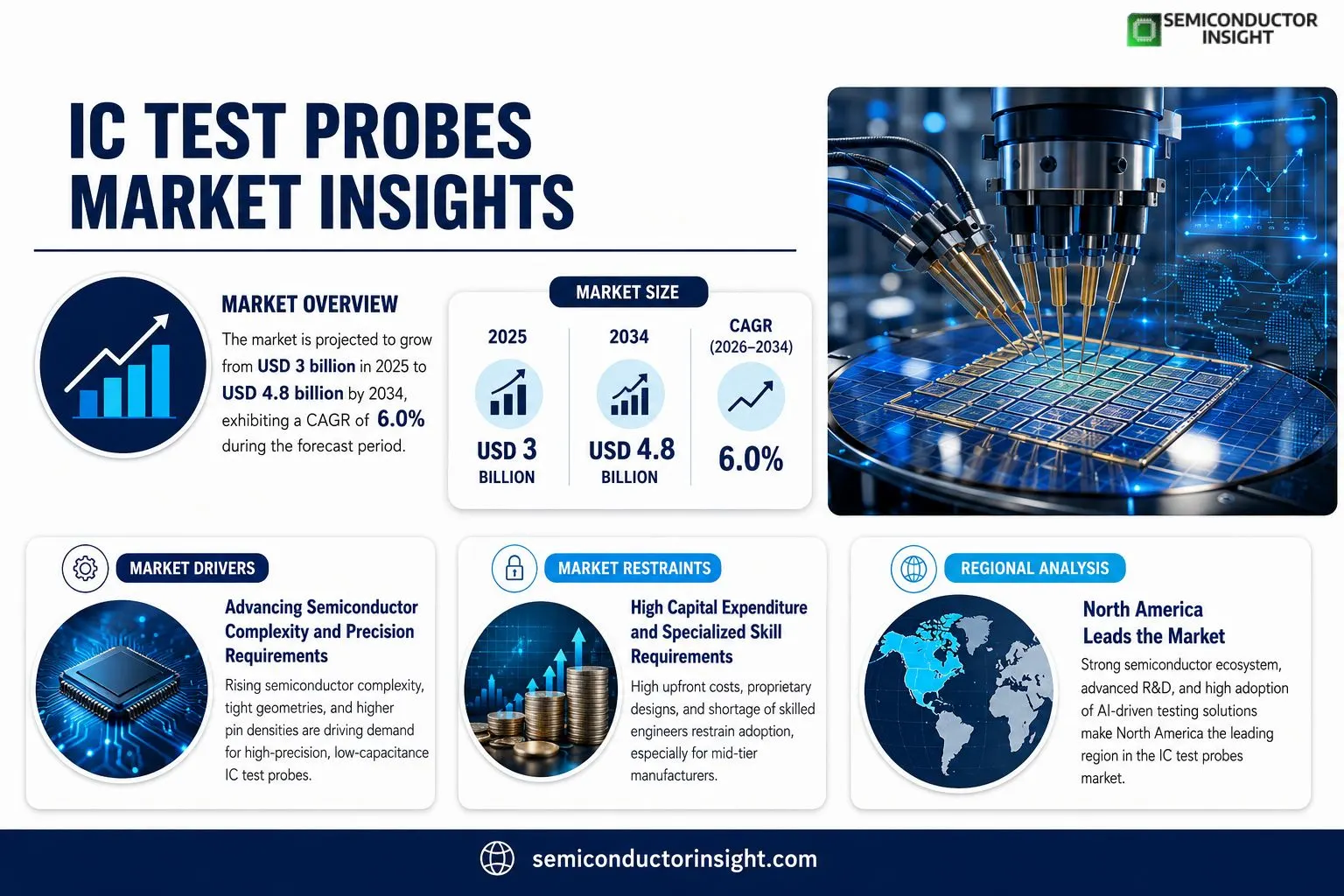
IC Test Probes Market size was valued at USD 3 billion in 2025 to USD 4·8 billion by 2034, exhibiting a CAGR of approximately six percent during the forecast period.
IC test probes are precision contact assemblies employed during wafer‑level testing of integrated circuits prior to packaging.They enable electrical connectivity between densely packed pads on silicon wafers and external measurement equipment.Modern probe cards incorporate MEMS‑based contact arrays
MARKET DRIVERS
Advancing Semiconductor Complexity and Precision Requirements
As integrated circuits evolve toward higher pin densities, deeper logic levels, and tighter power‑delivery networks, test practitioners demand probes that can interrogate increasingly miniature structures without compromising signal integrity. The proliferation of multi‑chip modules and system‑in‑package configurations amplifies the need for high‑resolution, low‑capacitance probes capable of handling densely packed pads while preserving die‑bond integrity. In the IC Test Probes Market, these engineering demands translate directly into higher initial capital outlays for probe card designs that support finer pitch and adaptive contact force control. Simultaneously, manufacturers increasingly rely on automated test equipment (ATE) that couples advanced probe cards with sophisticated test sequences, thereby pushing the architecture of probe card materials toward temperature‑stable alloys and flexible circuitry that can tolerate higher test frequencies. Over the forecast period, we anticipate a composite annual growth exceeding 6 % driven by the introduction of 3 nm and sub‑3 nm process nodes, which elevate test reliability expectations and underscore the necessity for next‑generation probe solutions.
Evolving Manufacturing Standards and Yield Optimization
In the IC Test Probes Market, stringent automotive and aerospace certification regimes now require probes to withstand elevated vibration, temperature cycling, and electromagnetic interference. The resulting shift toward ruggedized, high‑temperature compatible probe cards has compelled vendors to incorporate novel alloys and brazing techniques, cultivating a competitive differentiation between standard, cost‑effective probes and specialty, high‑reliability alternatives. Concurrently, semiconductor fabs pursue yield improvements by implementing high‑throughput test programs that reduce cycle times. By integrating real‑time pad‑contact verification and adaptive probe addressing, probe solutions can shorten downtimes and reduce test wall‑clock duration, offering a tangible margin impact across the silicon value chain. Moreover, the adoption of design‑for‑test (DfT) methodologies that embed test structures directly into the die layout creates simultaneous opportunities for probe developers to design hybrid probe cards that accommodate both legacy and advanced test functionalities. The coupling of these trends establishes a clear pathway for market growth fueled by both compliance mandates and cost‑optimization imperatives.
➤ Probe cards that can accommodate shifting pin counts reduce test cycle time dramatically.
From a strategic standpoint, firms that invest in design‑time collaboration with fab owners to co‑develop probe‑card libraries can capture early market share and secure long‑term service contracts. The need to protect intellectual property during probe card development further accelerates the shift toward modular, reusable probe platforms that lower engineering turnaround. Consequently, vendors that expedite the prototyping phase, leverage digital twin modeling, and offer rapid certification pathways are positioning themselves to capture the majority of the IC Test Probes Market as the industry accelerates toward higher density, higher frequency, and stricter reliability requirements.
MARKET CHALLENGES
Rising Visibility of Probe Alignment Errors and Test Anomalies
Despite advancements in probe technology, alignment inaccuracies remain a persistent source of test failures across both discrete and system‑in‑package silicon lines. The cumulative effect of probe wear, pad discretization defects, and thermal expansion can create contact misalignments that manifest as erratic test results, forcing re‑runs and inflating test cycle costs. In the IC Test Probes Market, the lack of a global standard for probe alignment tolerances further complicates quality assurance, especially for multi‑vendor manufacturing ecosystems. Consequently, test engineers must invest in routine probe‑card calibration, often employing optical inspections or touch‑probe verification, which introduces operational overhead and potential downtime.
Other Challenges
High Cost and Rapid Obsolescence
The capital expenditure required for high‑end probe cards, coupled with the swift obsolescence cycle driven by emerging process nodes, can strain vendor margins. Modalities that rely on incremental upgrades tend to elevate the total cost of ownership for large enterprises, pushing them toward alternative test approaches such as in‑silico testing or machine‑learning driven failure analysis.
Limited Standardization Across Platforms
The absence of a unified probe card specification across semiconductor families leads to fragmented tooling investments and complicates cross‑fabric test strategy development. Manufacturers often must maintain multiple probe cards for different yield lines, escalating inventory costs and making it difficult to achieve economies of scale in the IC Test Probes Market.
Supply Chain Volatility and Component Scarcity
Critical probe card materials, including high‑grade alloy contacts and specialized epoxy resins, are subject to geopolitical trade restrictions and limited vendor pools. This concentration can result in price spikes and delivery delays, jeopardizing strict production schedules and making demand forecasting volatile.
MARKET RESTRAINTS
High Capital Expenditure and Specialized Skill Requirements
One of the foremost restraints confronting the IC Test Probes Market is the substantial upfront investment required to develop, manufacture, and maintain probe card fleets that can keep pace with advancing process geometries. The necessity for highly specialized engineering talentparticularly in materials science and micro‑assemblyfurther compounds deployment costs, as firms must recruit and retain skilled personnel capable of executing precision alignment, fatigue testing, and reliability validation. Additionally, the industry’s reliance on proprietary designs and patents creates a barrier to entry for smaller players, limiting competitive dynamics and enabling incumbents to cement their market positions. Combined, these factors dampen adoption rates, especially among mid‑tier manufacturers that lack the capital reserves to invest in state‑of‑the‑art probe infrastructure, thereby stalling broader market expansion. A pragmatic approach to mitigating these constraints involves adopting modular, plug‑and‑play probe architectures that enable incremental upgrades, licensing of technology platforms, or shared‑service agreements that distribute cost burdens across multiple clients.
MARKET OPPORTUNITIES
Exploring Digital Twin Integration and Predictive Maintenance
Emerging digital twins of probe card assemblies present tangible opportunities for firms operating within the IC Test Probes Market to differentiate themselves by offering predictive maintenance services that lower overall lifecycle costs for customers. By embedding sensor networks into probe cardsmonitoring parameters such as contact force, temperature variance, and micro‑crack propagationvendors can generate real‑time analytics that anticipate degradation before it leads to test failures. This capability not only enhances reliability but also creates recurring revenue streams through subscription‑based monitoring platforms. Moreover, the convergence of artificial intelligence with test data enables automated root‑cause analysis, reducing engineer time spent on troubleshooting and accelerating time‑to‑market for new silicon assets. Firms that invest early in the development of open‑source digital twin frameworks will likely capture a prominent share of this nascent sub‑market, positioning themselves as technology leaders in an ecosystem that increasingly values data‑driven decision making.
IC Test Probes Market Trends
Rise of MEMS‑Based IC Test Probes
The IC Test Probes Market is experiencing a decisive shift toward MEMS‑derived solutions that reconcile the demands of high‑density layouts with robust durability. MEMS probes deliver sub‑micron tip resolution, lightweight construction, and configurable thermal behavior while consuming a fraction of the fixture space required by conventional metal probes. As system‑on‑chip designs push contact pads to tighter tolerances, the industry increasingly relies on MEMS solutions that avoid mechanical stress and extend fixture life. The resulting lower test cycle costs and accelerated process windows align with the efficiency goals held by OEMs, creating a clear revenue vector for MEMS manufacturers that outpaces legacy probe vendors.
Other Trends
Sustainable Probe Materials and Lifecycle Management
Environmental compliance has crystallised as a differentiator in probe selection. Companies now produce probes from recyclable polymers, heat‑set epoxy composites, and low‑toxicity adhesives, trimming hazardous waste footprints in line with the EU’s WEEE directive and U.S. EPA regulations. Modularity in probe design enables replacement of individual components rather than entire fixtures, curtailing scrap volumes and fostering planned obsolescence strategies that extend asset life. The economic upside is tangible: operators lower replacement frequency costs while maintaining qualification depth across multiple applications, thereby tightening the cost structure of test services.
Advancement of Integrated Multi‑function Probes
Complementing the MEMS and sustainability narratives, the market is witnessing the proliferation of integrated multi‑function probes that amalgamate test, debugging, and calibration capabilities into a single interface. These solutions minimise tool‑swap downtime, collapse labor hours, and provide real‑time diagnostics during design iterations. Their prominence spans high‑speed digital and RF subsystems, where tolerance for tester configuration errors narrows. Suppliers that embed electromagnetic shielding, programmable tip profiles, and temperature control features into a unified probe package tap into a customer segment that prioritises engineering service agility and reduced time‑to‑market.
COMPETITIVE LANDSCAPEKey Industry Players
At the apex of the IC test probe segment sits JC Cherry, Inc., whose consolidated revenues of $600 million in 2023 position it ahead of its peers and give it a dominance that translates into a high share of the high‑end MEMS and optoelectronic probe market. The company’s leveraged supply‑chain integrationowning both probe head manufacturing and fixture assemblypermits price discipline that keeps competitors at bay. Additionally, its focus on next‑generation high‑frequency probes is supported by a portfolio of patents that extends the usable life of probe packages, giving its clients a measurable margin advantage in ultra‑high‑speed use cases. This strength is underscored by recent contracts with tier‑1 semiconductor OEMs that span both tabletop and wafer‑scale environments, illustrating the company’s appetite for pushing the envelope in probe performance. The company’s emphasis on sensor integration, particularly for automotive laser modules, also feeds into the broader trend of in‑fab test automation. Its recent acquisition of a micro‑electromechanical probe division has further strengthened its position across high‑temperature application domains.Niche but technically sophisticated players such as Ironwood Electronics, QA Technology and Burndy contribute depth to the market. Ironwood’s silicon‑based probe solutions are engineered for extreme thermal cycling, making them attractive for automotive electronics, while QA Technology’s modular probe heads allow rapid configuration changes across product familiesa feature that resonates with design‑intellectual firms. Burndy, with its long history in electromechanical connectors, has recently broadened its footprint into MEMS probing by adding a line of high‑precision motion platforms. Materion Barr Precision Optics, Rika Denshi and YAMAICHI ELECTRONICS, each bring niche fabrication capabilitiesoptical coatings, high‑precision alignment, and hybrid probe architecture respectivelythat serve specialty segments such as photonics and sensor ICs. Commercially, these players create a landscape where differentiation is driven more by addressing specific embodied‑functionality needs than by price, ensuring a lower market concentration and fostering steady sign‑off rates for new technologies as OEMs move toward dense packaging. Meanwhile, the niche segment remains open to disruptors like new entrants leveraging additive manufacturing to reduce probe lead times. The heterogeneity of supply chains across these players also motivates collaborative standards development.
List of Key IC Test Probes Companies Profiled
- JC Cherry, Inc.
- JC Cherry, Inc.
- CFE Corporation Co., Ltd.
- CFE Corporation Co., Ltd.
- GGB Industries, Inc.
- GGB Industries, Inc.
- Interconnect Devices, Inc.
- Interconnect Devices, Inc.
- Sumitomo Electric USA, Inc.
- Ironwood Electronics, Inc.
- QA Technology Company, Inc.
- Burndy LLC
- Materion Barr Precision Optics & Thin Film Coatings
- Rika Denshi America Inc.
- YAMAICHI ELECTRONICS Deutschland GmbH
- Unitechno USA, Inc.
Segment Analysis:
| Segment Category | Sub-Segments | Key Insights |
| By Type |
|
LED Probes dominate the first segment, offering exceptional signal integrity for high‑frequency IC tests. Their low contact resistance and minimal heat generation enable reproducible measurements even in tight geometries. Key strengths include:
|
| By Application |
|
Integrated Circuit probes lead the application segment, driven by the proliferation of high‑performance microprocessors and integrated memory. They provide high‑precision electrical contact and rapid test cycles, and they are crucial for design validation and yield optimization. Main attributes:
|
| By End User |
|
Test & Measurement users drive the segment, as they require probes that combine speed, reliability, and ease of integration into automated test stations. The value proposition focuses on minimizing test cycle times while maintaining data integrity across varied chip technologies. Key elements include:
|
| By Package Type |
|
Chip‑on‑Board (COB) probes take the lead as they align closely with automotive and consumer electronics trends that favor minimal parasitic inductance. Their compact design allows dense test pad arrays and high‑speed signal capture, with features such as low insertion loss and excellent thermal stability. Advantages:
|
| By Integration Method |
|
Flip Chip integration probes lead the segment, as the method provides superior electrical performance and mechanical robustness for advanced chip designs. They support high‑bandwidth routing and reduce parasitic inductance, meeting the demands of mobile and high‑speed computing markets. Key benefits:
|
Regional Analysis: IC Test Probes Market
North America
North America remains the dominant segment in the IC Test Probes Market, largely due to the sustained pace of semiconductor development across the United States and Canada. The region’s concentration of world‑class semiconductor fabs, supported by government initiatives that favor advanced packaging and AI‑driven design, keeps the demand for high‑precision probes steady. The northern local supply chain is tightly integrated, allowing rapid prototyping and iterative testing that drives both current production volumes and future capacity planning.Challenges are less about supply constraints and more about skill shortages; specialised probe engineers are sparsely available, pushing firms towards automation and AI‑assisted diagnostics. This influx of digital tools has begun to reshape test methodologies, forcing a shift from traditional multipurpose probes to more bespoke solutions for 3D‑IC and system‑on‑chip structures. Companies that are early adopters of hybrid or multi‑parameter probes retain a competitive edge, as these devices can simultaneously measure electrical, mechanical, and thermal properties during a single test run.
Market share is bolstered by the high concentration of high‑end market players in the United States, many of whom are investing heavily in probe technology R&D to maintain a lead in competitive design cycles. These firms are also partnering with equipment manufacturers to embed probing solutions into wider test and measurement ecosystems, thereby expanding their footprint beyond pure probe sales. The trajectory for the next decade will likely follow a “test‑as‑a‑service” model, with subscription‑based solutions becoming a viable revenue stream for probe manufacturers that can offer turnkey test platforms.
Overall, North America’s dominance is reinforced by a convergence of regulatory support, investment in research, and a maturing ecosystem that values iterative improvement. The region’s ability to innovate in probe manufacturing technology positions it well to absorb the forthcoming shift toward more complex IC architectures and the emergent demand for sustainable, low‑energy probing solutions.
The region’s rapid adoption of AI‑enabled design tools requires high‑resolution probes that can capture detailed signal integrity data. Coupled with an established network of last‑mile testing facilities, this creates a continuous demand for precise, low‑distortion test probes that can operate across wider frequency ranges without sacrificing yield.
Market concentration is carried by a handful of global players headquartered in the United States who dominate through patented probe geometries and superior miniaturisation. Smaller entrants focus on niche segments, such as RF probes for wireless modules, creating a subtle but steady diversification.
Talent scarcity remains a notable bottleneck; universities lag in advanced probe‑design curricula, pushing companies to form strategic partnerships with specialised training institutions or invest in in‑house R&D. Supply‑chain resilience is another concern, as rare‑earth components for probe assemblies can experience intermittent shortages.
The next five years are likely to see a pivot toward green probe technologies that lower power draw during test cycles, addressing tightening environmental regulations and cost‑control pressures. Anticipated integration of edge‑computing capabilities within test consoles will also reshape how probes collect and process data on‑the‑fly.
Europe
Europe’s IC Test Probes Market is anchored by a strong tradition of precision engineering and a growing emphasis on high‑performance computing. Nations like Germany and France invest heavily in test equipment manufacturing, fostering a domestic ecosystem that balances proprietary probe designs with open‐source collaboration. The region’s regulatory environment prioritises sustainability; consequently, manufacturers are experimenting with alternative, eco‑friendly materials for probe connections to reduce hazardous waste. While the overall market size is smaller than that of North America, European firms are carving out a niche within advanced packaging solutions for automotive electronics, where reliability and low thermal stress are paramount. The anticipated shift towards multi‑functional probes is also observable, as electronic design automation platforms in the region increasingly support integrated test strategies that combine electrical, mechanical, and thermal measurements.
Asia-Pacific
Asia‑Pacific stands out as a rapidly developing destination for IC Test Probes, especially within Japan, South Korea, and the Greater China region. The concentration of initial‑design and fabrication facilities fuels a robust demand for probe systems capable of handling ever‑smaller process nodes. Manufacturers there are focusing on scaling probe density while maintaining signal integrity, a balancing act critical for next‑generation memory and logic devices. In addition, market participants are investing in AI‑auto‑diagnostics to streamline setup times, reflecting a broader industry trend toward digital acceleration. Though the region grapples with supply‑chain volatility, its large domestic market mitigates exposure to global disruptions.
South America
South America is characterised by a modest but steadily growing probe market, primarily driven by the expansion of semiconductor assembly plants in Brazil and Chile. The region’s strategy hinges on integrating probe solutions with step‑and‑repeat test processes to accommodate heterogeneous integration. A key factor is the growing partnership between local OEMs and international probe suppliers, which facilitates technology transfer and capacity building. Despite limited local R&D, South American companies are increasingly participating in global design initiatives, positioning themselves as flexible, cost‑effective partners for firms seeking to diversify supply chains.
Middle East & Africa
The Middle East and Africa segment is unique in that it is undergoing a structural transformation from a commodity‑focused market to one that values advanced IC testing capabilities. Strategic investments by national governments in high‑tech zones in Saudi Arabia, UAE, and South Africa are spurring the establishment of new test fabs, thereby increasing demand for high‑resolution probes. The market here is distinctive due to its dual focus on renewable energy systems and aerospace electronics, sectors that demand rigorous testing for safety and reliability. Adoption of modular probe designs, supported by governmental incentives, is accelerating, helping firms reduce time‑to‑market. While the overall volume remains moderate, the pace of technological uptake suggests a strong upward trajectory in probe spend over the next decade.
Report Scope
This market research report provides a comprehensive analysis of the IC Test Probes Market , covering the forecast period 2026–2034. It offers detailed insights into market dynamics, technological advancements, competitive landscape, and key trends shaping the industry.
Key focus areas of the report include:
- Market Overview: The report begins with an overview outlining its current market scenario, key growth indicators, and industry transformation drivers. It discusses macroeconomic factors, demand–supply balance, regulatory landscape, and the strategic role of semiconductors in powering advancements across industries such as automotive, telecommunications, consumer electronics, and industrial automation.
- Market Size & Forecast: Historical data and future projections for revenue, unit shipments, and market value across major regions and segments.
- Segmentation Analysis: Detailed breakdown by product type, technology, application, and end-user industry to identify high-growth segments and investment opportunities.
- Regional Insights: Insights into market performance across North America, Europe, Asia-Pacific, Latin America, and the Middle East & Africa, including country-level analysis where relevant.
- Competitive Landscape: Profiles of leading market participants, including their product offerings, R&D focus, manufacturing capacity, pricing strategies, and recent developments such as mergers, acquisitions, and partnerships.
- Technology Trends & Innovation: Assessment of emerging technologies, integration of AI/IoT, semiconductor design trends, fabrication techniques, and evolving industry standards.
- Market Drivers & Restraints: Evaluation of factors driving market growth along with challenges, supply chain constraints, regulatory issues, and market-entry barriers.
- Stakeholder Insights: Insights for component suppliers, OEMs, system integrators, investors, and policymakers regarding the evolving ecosystem and strategic opportunities.
Primary and secondary research methods are employed, including interviews with industry experts, data from verified sources, and real-time market intelligence to ensure the accuracy and reliability of the insights presented.
FREQUENTLY ASKED QUESTIONS:
What is the current market size of IC Test Probes Market?
-> IC Test Probes Market size was valued at USD 3 billion in 2025 to USD 4·8 billion by 2034, exhibiting a CAGR of approximately six percent during the forecast period
Which key companies operate in IC Test Probes Market?
-> Key players include JC Cherry, Inc., Ironwood Electronics, Inc., QA Technology Company, Inc., Burndy LLC, CFE Corporation Co., Ltd., among others.
What are the key growth drivers?
-> Key growth drivers include increasing demand for high‑density packaging, growth of AI‑enabled testing, and expansion of semiconductor manufacturing capacity.
Which region dominates the market?
-> Asia-Pacific is the fastest‑growing region, while Europe remains a dominant market.
What are the emerging trends?
-> Emerging trends include integration of micro‑LED probes, MEMS‑based probing solutions, and AI‑driven test automation.
What are the primary market segments by type?
-> The market is segmented into LED Probes, MEMS Probes, Vertical Probes, and Others.
What applications drive the IC Test Probes market?
-> Major applications include Integrated Circuits, Discrete Devices, Optoelectronic Devices, Sensors, and Other specialty devices.
What is the forecasted CAGR for the market?
-> The market is projected to grow at a CAGR of 5.6% from 2024 to 2031.
Who are the top three revenue‑generating companies in 2024?
-> JC Cherry, Inc., Ironwood Electronics, Inc., and QA Technology Company, Inc. topped the revenue rankings in 2024.
What is the base year used for the analysis?
-> The analysis uses 2020 as the base year for historical comparisons.
What methodology underpins the report?
-> The report employs a combination of primary interviews, secondary data collection, and quantitative modeling to derive forecasts.
What are the key benefits of this report?
-> Benefits include actionable insights, detailed segmentation, and forward‑looking market forecasts that aid strategic decision‑making.
How have prices of IC Test Probes evolved (2020‑2025)?
-> Prices have shown a moderate increase of 3‑4% CAGR driven by raw‑material cost pressures and technology upgrades.
What are the main market restraints?
-> Restraints comprise supply chain disruptions, high R&D costs, and stringent quality standards.
Get Sample Report PDF for Exclusive Insights
Report Sample Includes
- Table of Contents
- List of Tables & Figures
- Charts, Research Methodology, and more...
 Download Sample Report PDF




