
Key Statistics
Key Takeaways
- MEMS Probe Cards are the preferred emerging architecture in the source-page segmentation because advanced logic, HBM and 3D integration require tighter pitch, higher contact counts and better electrical control than conventional cantilever approaches can provide at the most demanding nodes.
- Foundry & Logic drives the majority of source-page innovation because wafer-level screening becomes more valuable as die size and downstream packaging cost increase. HBM and DRAM are also major growth areas, with FormFactor reporting record DRAM revenue and strength in HBM probe-card demand in 2026.
- Asia Pacific is used as the largest market because the source-page FAQ explicitly says Asia holds the largest share, supported by China, Japan, South Korea and Taiwan. A separate regional passage says North America retains leadership, so that inconsistency is recorded rather than silently resolved.
- Manufacturing capacity is expanding materially. Technoprobe raised planned capital expenditures through the first quarter of 2027 to about €350 million after H1 2026 revenue rose 42.4%, while FormFactor expanded its Taiwan manufacturing partnership with Keystone Microtech.
- The source-page CAGR does not reconcile with the headline size anchors. USD 3.324 billion in 2025 and USD 6.940 billion in 2034 imply approximately 8.5% annual compound growth, not the printed 9.1%; the anchor-derived rate is used for the 2026 estimate and all repeated figures.
Probe Card Market Overview
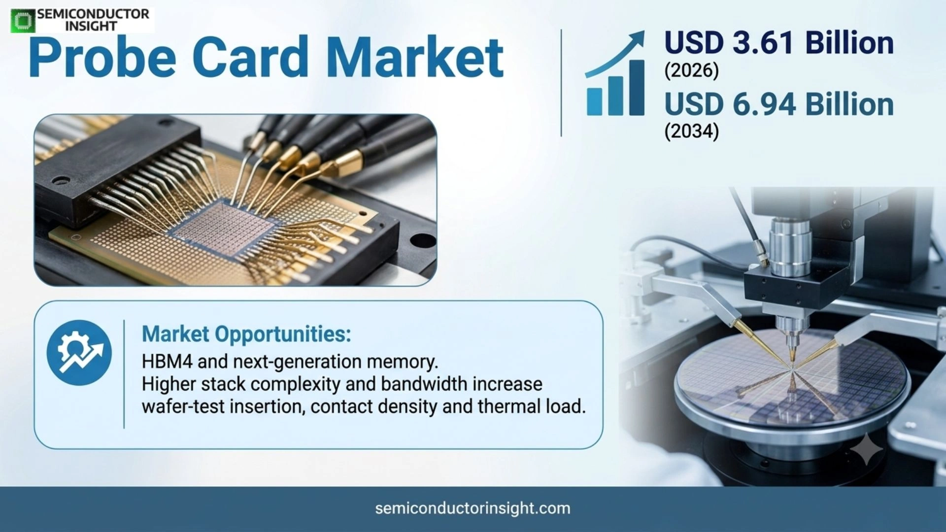
Probe Card Market is valued at USD 3.32 billion in 2025, increases to an estimated USD 3.61 billion in 2026, and is projected to reach USD 6.94 billion by 2034. The selected source-page size anchors imply a 8.5% CAGR during 2026–2034. Asia Pacific is the largest market in 2025 based on the source-page FAQ, while the source regional narrative separately calls North America a leader, while current demand is being reshaped by AI and high-performance computing, HBM and advanced memory, sub-5 nm logic, 2.5D/3D packaging, higher pin counts, tighter pitches, higher-frequency wafer test and the expansion of test-interface manufacturing capacity in Taiwan, China and other semiconductor hubs.
Probe cards are custom electromechanical interfaces that connect automatic test equipment to pads, bumps or micro-bumps on semiconductor wafers before individual dies are packaged. A probe card must make thousands to tens of thousands of reliable contacts while controlling force, alignment, impedance, leakage and thermal behavior. As chip value and packaging complexity rise, early wafer-level test becomes economically more important because defective dies can be rejected before they consume advanced substrates, HBM stacks or expensive assembly steps.
The market is being reshaped by AI and high-bandwidth memory. Technoprobe reported first-half 2026 revenue of €464.1 million, up 42.4% year over year, with management citing AI-driven volumes and increasing testing intensity per wafer. FormFactor reported record second-quarter revenue of USD 258.2 million and said HBM demand drove probe-card growth. These supplier results provide primary evidence that test-interface spending is rising alongside advanced memory and compute complexity rather than merely following wafer volumes.
Probe-card technology is also becoming more regionalized. FormFactor and Keystone Microtech expanded a strategic partnership in Taiwan in July 2026 to improve manufacturing scalability and local support, while Technoprobe completed a China partnership in August involving a USD 35 million local investment in Nexprobe Semiconductor Shanghai. Such moves matter because probe cards are custom-built, frequently serviced and closely co-developed with fabs, so proximity can shorten feedback, repair and qualification cycles.
Segment Analysis: By Type
The source page segments the market into Cantilever Probe Card, Vertical Probe Card, MEMS Probe Card and Others. MEMS is identified as the preferred architecture for high-density advanced-node testing, while vertical and cantilever designs remain economically important for mature logic, memory, power, analog and specialty products that do not require the highest contact density.
| Type | Technical / commercial role | Market position |
|---|---|---|
| Cantilever Probe Card | Cantilever cards use angled needle probes extending from a support structure and remain common for analog, power, RF and mature-node devices. They are relatively flexible to customize and can be cost-effective for lower pin counts or larger pad pitches. Performance depends on needle metallurgy, planarity, scrub behavior and stable contact resistance over repeated touchdowns. | Established segment with durable mature-node demand. Cantilever cards compete primarily on cost, serviceability and application-specific geometry rather than maximum contact density, making them relevant to industrial, automotive and specialty semiconductor programs with long lifecycles. |
| Vertical Probe Card | Vertical architectures arrange probes approximately perpendicular to the wafer surface, supporting higher pin density and more uniform contact mechanics than traditional cantilever systems. They are widely used in memory and advanced logic testing where many contacts must be controlled simultaneously across a large probe area. | Large advanced-test segment. Vertical designs remain central for DRAM, NAND and logic because they can balance high pin count, current capability and maintainability. Suppliers differentiate through probe materials, ceramic or organic interposers, thermal behavior and field-repair capability. |
| MEMS Probe Card | MEMS probe cards use microfabricated contact structures that can achieve extremely fine pitch, controlled geometry and high repeatability. They are suited to HBM, advanced logic, 2.5D/3D and high-frequency applications where very dense bumps and tight electrical performance are required. Production demands cleanroom microfabrication and sophisticated design automation. | Fastest technology shift in the source page. AI accelerators and advanced memory increase the value of MEMS because contact count and pitch rise faster than traditional architectures can comfortably support. The segment benefits from proprietary process IP and high qualification barriers. |
| Others | Other architectures include specialty RF/mmWave, parametric, optical and application-specific probing solutions that may combine coaxial structures, spring contacts, advanced substrates or modular interfaces. These are lower-volume but can carry high value because they solve difficult electrical or mechanical test problems. | Specialty premium segment. Growth is tied to silicon photonics, RF front ends, automotive radar and research applications where signal bandwidth, low leakage or unusual pad geometry is more important than high-volume standardization. |
Secondary segmentation: By Technology
The source page further divides test architectures into 2D, 2.5D and 3D. The commercial distinction is the interconnect density and package architecture that must be accessed during wafer-level test. 3D technology creates the most demanding probe requirements because stacked dies and through-silicon-via structures require dense, uniform access before expensive integration steps.
| Technology | Commercial implication |
|---|---|
| 2D | Conventional planar devices continue to represent a large installed base across analog, power, microcontrollers and mature logic. Probe cards can use established cantilever, vertical or MEMS solutions depending on pad pitch and frequency. Growth follows wafer volumes and product refresh rather than a radical change in test architecture. |
| 2.5D | Interposers and chiplet platforms increase die value before final assembly and often introduce dense micro-bump interfaces. Wafer-level known-good-die screening becomes more important because one bad die can compromise a multi-chip package. Probe cards therefore need more contacts, tighter pitch and stronger power delivery. |
| 3D | 3D integration and HBM stacking require very fine-pitch testing of stacked or stack-ready components, often under stringent thermal and current conditions. MEMS architectures gain importance because mechanical uniformity and electrical integrity must be controlled across many thousands of contacts. |
Secondary segmentation: By End User
The source page identifies Semiconductor Manufacturers, Test Equipment Providers and Integrated Device Assemblers. Semiconductor manufacturers are the principal direct users because wafer probing is embedded in fab test flows, while test-equipment providers and assemblers influence mechanical and electrical interface specifications. For probe-card suppliers, the commercial implication is that engineering capacity, contact density, repair turnaround and customer qualification determine saleable output more directly than simple factory floor area or semiconductor unit growth.
| End user | Demand characteristics |
|---|---|
| Semiconductor Manufacturers | Foundries and IDMs qualify cards against specific wafers, testers and temperature conditions. The relationship is highly technical and recurring because each new chip generation or package architecture can require a new custom card. Yield learning and service response are therefore major supplier-selection factors. |
| Test Equipment Providers | ATE and prober vendors work with probe-card companies to ensure signal integrity, thermal control and mechanical compatibility. Partnerships can accelerate deployment because advanced test performance depends on the complete tester, probe card, probe station and software stack rather than one component alone. |
| Integrated Device Assemblers | OSATs and advanced packaging companies need known-good-die test before chiplet, HBM and 3D assembly. Their demand is rising as more electrical screening occurs between wafer fabrication and final package test, creating opportunities for modular high-density probe solutions. |
Secondary segmentation: By Sales Channel
The source page separates Direct Sales and Distribution and states that direct sales are gaining traction among leading fab customers. This pattern is consistent with the highly customized nature of probe cards, which require application engineering, rapid repair and continuous feedback from process and test teams. This matters because each advanced card is matched to a specific wafer, tester and electrical requirement, so design-in and service responsiveness can protect revenue over the full device ramp even when competitors offer similar basic architectures.
| Sales channel | Commercial role |
|---|---|
| Direct Sales | Large foundries and memory IDMs usually work directly with probe-card engineering teams because the card is custom to a device and often evolves during product ramp. Direct relationships support faster debugging, controlled IP exchange and service contracts, creating sticky recurring revenue. |
| Distribution | Distribution is more relevant for standard probes, accessories, regional service and lower-volume specialty customers. It can improve local coverage but is less suitable for the most advanced custom cards where detailed co-design and fab access are essential. |
Segment Analysis: By Application
By application, the source page lists Foundry & Logic, DRAM, Flash, Parametric and Others (RF/MMW/Radar, etc.). Foundry & Logic is identified as the main innovation driver, while HBM has made DRAM probing especially important in 2026 because stacked memory increases test intensity before expensive packaging and integration. Buyers therefore evaluate planarity, contact resistance, signal integrity, current capacity, thermal behavior and regional support together, rather than treating a probe card as an interchangeable mechanical accessory.
| Application | Demand characteristics |
|---|---|
| Foundry & Logic | Advanced logic dies become more expensive as node complexity and die size increase, so early wafer screening has high economic value. Probe cards must handle fine pitch, high current and high-frequency interfaces while remaining stable across wafer temperature. Networking and AI-related logic contributed to strong FormFactor foundry/logic demand in 2026. |
| DRAM | DRAM probe cards test large arrays of memory dies and increasingly support HBM workflows. HBM adds tight pitch, high bandwidth and known-good-die requirements before stacking, making probe-card performance a direct contributor to package yield. FormFactor reported record DRAM revenue in Q1 2026 and continued HBM strength in Q2. |
| Flash | NAND and embedded flash require high parallelism and reliable contact across many memory dies. Mature vertical cards remain important, while advanced NAND and enterprise-storage products increase test complexity through higher layer counts and density. Volume economics make card lifetime and maintenance cost especially important. |
| Parametric | Parametric cards support process-control and device-characterization measurements such as leakage, threshold voltage and line resistance. They prioritize low leakage, precision and stable electrical behavior rather than maximum pin count, serving fabs, R&D and process-development teams. |
| Others (RF/MMW/Radar, etc.) | RF, millimeter-wave, radar, silicon photonics and specialty sensor devices require calibrated high-frequency or optical probing. Contact structures, cables and substrates must preserve impedance and reduce parasitics, creating a premium niche that grows with 5G/6G, automotive radar and co-packaged optics. |
Regional Analysis
The source page is internally inconsistent on regional leadership: its FAQ states that Asia holds the largest share, while the detailed North American section says North America retains leadership. This article uses Asia Pacific for the 2025 leadership card because the FAQ gives the clearest explicit global ranking, while North America is treated as a high-value innovation and customer-design center.
Why does probe-card leadership differ between manufacturing scale and advanced-test influence?
Asia Pacific contains the largest concentration of leading foundries, memory fabs and semiconductor packaging, so it creates the largest physical demand base and increasingly hosts local card manufacturing. North America has major AI, logic and test-technology suppliers and drives sophisticated design requirements. Europe contributes Technoprobe and automotive/industrial semiconductor expertise. South America and MEA remain niche because wafer fabrication is limited, although specialized test demand can emerge around new semiconductor and defense initiatives.
| Region | Position | Growth outlook | Demand profile | What decides supplier selection |
|---|---|---|---|---|
| Asia Pacific | Largest source-page market | High | Foundry, memory and packaging-led | Local service, high-density capability and manufacturing scale |
| North America | Innovation and design hub | High | AI, foundry/logic and systems-led | Electrical performance, co-design and service |
| Europe | Technology supplier stronghold | Moderate to high | Probe-card production, automotive and industrial-led | Precision engineering, IP and global customer access |
| South America | Niche | Low to moderate | Assembly, specialty electronics and research-led | Imported supply, flexibility and service |
| Middle East & Africa | Emerging niche | Low from small base | Defense, data-center and semiconductor initiatives-led | High reliability, import access and local support |
Competitive Landscape
The source page contains three different company sets: a short public profile list, a broader FAQ list and a formal Table of Contents with eighteen manufacturer profiles. To preserve the deepest source structure, this article uses the formal TOC profile list in exact order: FormFactor, Technoprobe, Micronics Japan, Japan Electronic Materials, MPI, SV Probe, Microfriend, Korea Instrument, Will Technology, TSE, Feinmetall, Synergie Cad Probe, TIPS Messtechnik, STAr Technologies, MaxOne, Shenzhen DGT, Suzhou Silicon Test System and CHPT.
Technoprobe and FormFactor are the clearest current scale leaders in advanced probe cards. Technoprobe’s H1 2026 revenue growth and increased capex demonstrate strong AI-driven demand and manufacturing expansion, while FormFactor’s record Q2 2026 revenue reflects HBM and Foundry & Logic strength. Both companies are also localizing supply in Asia, where major customers need rapid service.
Micronics Japan, Japan Electronic Materials, MPI and SV Probe form an established group with strong memory, logic, RF and vertical-card capabilities. Korea Instrument, Will Technology and TSE participate in the Korean test ecosystem, while Feinmetall, Synergie Cad Probe and TIPS Messtechnik address European and specialty applications. Competitive positions vary by architecture, pad pitch and customer fab relationship rather than one uniform global product.
The formal source profile list also includes Microfriend, STAr Technologies, MaxOne, Shenzhen DGT, Suzhou Silicon Test System and CHPT. The public profile summary separately mentions Protec MEMS Technology, which is not part of the formal eighteen-company TOC. That inconsistency is retained in the workbook reviewer note instead of adding a nineteenth company to the formal profile list.
| Competitive tier | Companies | Why they matter |
|---|---|---|
| Global advanced-test leaders | FormFactor; Technoprobe S.p.A.; Micronics Japan (MJC); Japan Electronic Materials (JEM) | These suppliers compete for leading foundry, memory and advanced-packaging programs where dense contacts, electrical performance and rapid service are critical. Scale allows significant R&D and global support. |
| Established regional specialists | MPI Corporation; SV Probe; Microfriend; Korea Instrument; Will Technology; TSE; Feinmetall | These firms address memory, logic, RF or regional customer needs and can win through specialized architecture, local responsiveness and lower-cost manufacturing around major Asian or European semiconductor clusters. |
| Specialty / emerging participants | Synergie Cad Probe; TIPS Messtechnik GmbH; STAr Technologies, Inc.; MaxOne; Shenzhen DGT; Suzhou Silicon Test System; CHPT | These companies target specialized process windows or regional markets. Their opportunity expands as customers seek second sources and local support, but advanced MEMS entry requires significant process IP and qualification. |
Companies profiled in the report
The source-page formal manufacturer profiles are, in order: FormFactor; Technoprobe S.p.A.; Micronics Japan (MJC); Japan Electronic Materials (JEM); MPI Corporation; SV Probe; Microfriend; Korea Instrument; Will Technology; TSE; Feinmetall; Synergie Cad Probe; TIPS Messtechnik GmbH; STAr Technologies, Inc.; MaxOne; Shenzhen DGT; Suzhou Silicon Test System; CHPT. Through 2034, suppliers that combine fine-pitch MEMS technology with scalable manufacturing and local service in major fab clusters are positioned to capture more AI, HBM and advanced-packaging test intensity.
Production Capacity Analysis
Probe-card capacity is measured less effectively by factory floor area than by qualified contact capacity, MEMS fabrication throughput, automated assembly, repair capability and engineering resources. Every card is customized to a device, so a supplier can have physical manufacturing space but still be constrained by design, microfabrication, precision assembly or customer qualification. Current capital investment by Technoprobe and Taiwan localization by FormFactor show that saleable capacity is expanding in both equipment and regional support.
Technoprobe increased estimated capital expenditures through the first quarter of 2027 to approximately €350 million after strong H1 2026 results. The company had already spent about €90 million in the first six months of 2026 and said investment would focus on expanding manufacturing capacity and accelerating technology development. This directly supports higher output for AI-related and advanced test solutions.
FormFactor’s expanded partnership with Keystone Microtech is a capacity and service initiative rather than simply a sales agreement. The partnership is intended to enhance manufacturing scalability and regional operational support in Taiwan, where foundry, HBM and packaging customers require fast card delivery, repair and engineering response. Local capacity therefore improves both throughput and customer qualification speed.
Technology architecture determines capacity requirements. Cantilever and vertical cards use precision mechanical and ceramic or PCB assembly, while leading MEMS cards need microfabrication processes with much tighter tolerances. Advanced cards can exceed tens of thousands of contacts, so automated inspection, planarity measurement and repair become important throughput constraints in addition to probe fabrication itself.
Market Dynamics
Market growth is driven by AI/HPC, HBM, advanced packaging and rising test intensity, while restraints include custom-design complexity, materials cost, long qualification cycles and concentrated MEMS process know-how. Probe cards are consumable production interfaces, but they behave commercially more like engineered capital components because each high-end card is designed around a specific chip, tester and wafer process.
Market Drivers
| Driver | Directional impact* | Commercial mechanism |
|---|---|---|
| AI & HBM test intensity | High | Larger AI dies, stacked memory and expensive packaging increase the value of early wafer screening and the number of contacts required per card. |
| Advanced packaging | High | 2.5D/3D and chiplet architectures require known-good-die test and finer-pitch probing before assembly. |
| Sub-5 nm logic | High | Tighter pad pitch, high current and signal integrity raise technical requirements and favor MEMS architectures. |
| Regional fab expansion | Medium to High | New fabs and packaging lines in Asia and elsewhere create demand for nearby custom-card engineering and service. |
AI increases the economic value of wafer-level screening
AI accelerators are large, expensive dies that are often combined with HBM and advanced substrates. Discovering a defect only after packaging destroys far more downstream value than in a simple packaged chip. As a result, manufacturers allocate more attention to known-good-die and high-coverage wafer testing, increasing both card complexity and testing intensity.
HBM expands contact density and thermal requirements
HBM production requires repeated test points before and after stacking, and each generation raises bandwidth and interconnect density. FormFactor’s 2026 HBM-related probe-card growth and Technoprobe’s AI-driven volumes are primary evidence that advanced memory is a structural probe-card driver rather than a temporary consumer-cycle recovery. The market consequence is that nominal production capacity becomes meaningful only when a card design is electrically validated, mechanically stable and qualified by the customer for repeated high-volume wafer touchdowns.
Chiplets and 3D integration create more test insertion points
A multi-die package can combine logic, memory and I/O from different process nodes. Each component must be screened before expensive integration, and some intermediate package stages also need electrical access. This increases the number of specialized probe solutions required per finished system and creates demand for modular MEMS technologies. For probe-card suppliers, the commercial implication is that engineering capacity, contact density, repair turnaround and customer qualification determine saleable output more directly than simple factory floor area or semiconductor unit growth.
Regionalization rewards local service networks
Probe cards are repaired, cleaned and modified during product ramps. Taiwan and China partnerships by leading suppliers show that fab proximity can reduce downtime and improve engineering feedback. Local manufacturing is therefore a competitive tool even when core IP and design remain centralized. This matters because each advanced card is matched to a specific wafer, tester and electrical requirement, so design-in and service responsiveness can protect revenue over the full device ramp even when competitors offer similar basic architectures.
Market Restraints
| Restraint | Directional impact* | Commercial mechanism |
|---|---|---|
| Custom design & qualification | High | Each advanced chip can require a dedicated card, slowing reuse and requiring engineering effort before revenue starts. |
| Probe/material cost | Medium to High | Specialty probes, ceramics and high-frequency substrates can represent a large share of card cost and face raw-material volatility. |
| MEMS process barriers | High | Leading fine-pitch products require proprietary microfabrication and yield know-how, limiting the number of qualified suppliers. |
| Service/maintenance burden | Medium | Cards wear through repeated touchdowns and need cleaning, repair or probe replacement, requiring a distributed support organization. |
Every leading-edge design requires substantial customization
Probe cards are not universal. Pad or bump layout, current, signal frequency, tester interface and thermal environment vary by device. Engineering work begins before manufacturing and continues during wafer ramp, making revenue dependent on customer schedules and qualification rather than simple catalog availability. Buyers therefore evaluate planarity, contact resistance, signal integrity, current capacity, thermal behavior and regional support together, rather than treating a probe card as an interchangeable mechanical accessory.
High-end materials and substrates create cost pressure
Probes use tungsten, rhenium-tungsten, copper alloys and other specialized materials, while advanced cards rely on precision ceramics, PCBs and interposers. The source page states probes can represent roughly half of bill-of-material cost, so raw-material volatility can pressure gross margin when customer pricing is fixed. Through 2034, suppliers that combine fine-pitch MEMS technology with scalable manufacturing and local service in major fab clusters are positioned to capture more AI, HBM and advanced-packaging test intensity.
Fine-pitch MEMS know-how is difficult to reproduce
Sub-micron alignment and dense contact arrays require specialized cleanroom fabrication, lithography, plating and inspection. A new supplier can buy equipment but still face years of process-development and customer-qualification work before it can compete for HBM or advanced logic cards at production scale. The market consequence is that nominal production capacity becomes meaningful only when a card design is electrically validated, mechanically stable and qualified by the customer for repeated high-volume wafer touchdowns.
Service requirements limit geographic reach
A damaged or contaminated card can stop wafer testing, so customers need rapid cleaning, repair and replacement. Suppliers without nearby service centers may lose advanced programs despite competitive product performance, which raises the fixed cost of entering new semiconductor regions. For probe-card suppliers, the commercial implication is that engineering capacity, contact density, repair turnaround and customer qualification determine saleable output more directly than simple factory floor area or semiconductor unit growth.
Market Opportunities
HBM4 and next-generation memory
Higher stack complexity and bandwidth increase wafer-test insertion, contact density and thermal load. Suppliers with MEMS cards designed for high current and fine pitch can capture premium memory programs. This matters because each advanced card is matched to a specific wafer, tester and electrical requirement, so design-in and service responsiveness can protect revenue over the full device ramp even when competitors offer similar basic architectures.
Chiplet known-good-die testing
Advanced packages require each die to be screened before integration. Probe-card vendors can develop modular architectures for logic, I/O and memory chiplets and participate in more test stages per system. Buyers therefore evaluate planarity, contact resistance, signal integrity, current capacity, thermal behavior and regional support together, rather than treating a probe card as an interchangeable mechanical accessory.
High-frequency RF and co-packaged optics
5G/6G, radar and silicon photonics require low-loss interfaces that traditional DC-oriented cards cannot support. Specialized RF and optical probe products can command high ASPs and differentiate suppliers from commodity test interfaces. Through 2034, suppliers that combine fine-pitch MEMS technology with scalable manufacturing and local service in major fab clusters are positioned to capture more AI, HBM and advanced-packaging test intensity.
China and Taiwan localization
Technoprobe’s China partnership and FormFactor’s Taiwan manufacturing partnership show active investment in local capacity. Regional suppliers and global incumbents can capture growth by reducing service lead time and improving local customer collaboration. The market consequence is that nominal production capacity becomes meaningful only when a card design is electrically validated, mechanically stable and qualified by the customer for repeated high-volume wafer touchdowns.
Supply Chain Analysis
Probe alloys, ceramics & PCB materials
MEMS / mechanical probe fabrication
Card assembly, alignment & electrical validation
Fab qualification, operation & repair
Probe alloys, ceramics & PCB materials
Upstream materials include tungsten and rhenium alloys, beryllium-copper, ceramic substrates, high-frequency PCB laminates and connectors. Purity, mechanical fatigue and electrical properties determine contact life and signal performance. For probe-card suppliers, the commercial implication is that engineering capacity, contact density, repair turnaround and customer qualification determine saleable output more directly than simple factory floor area or semiconductor unit growth.
MEMS / mechanical probe fabrication
Suppliers form needles or microfabricated probes using precision machining, lithography, plating and micro-assembly. Advanced MEMS stages are capital and IP intensive because geometry must be repeatable across thousands of contacts. This matters because each advanced card is matched to a specific wafer, tester and electrical requirement, so design-in and service responsiveness can protect revenue over the full device ramp even when competitors offer similar basic architectures.
Card assembly, alignment & electrical validation
Probes are integrated with interposers, PCBs and stiffeners and then characterized for planarity, force, leakage and signal integrity. Automated placement and metrology are essential as pitch shrinks and channel counts rise. Buyers therefore evaluate planarity, contact resistance, signal integrity, current capacity, thermal behavior and regional support together, rather than treating a probe card as an interchangeable mechanical accessory.
Fab qualification, operation & repair
Cards are matched to specific testers and wafers, qualified in production and serviced throughout the device lifecycle. Cleaning, repair and re-probing generate recurring service demand and make local engineering centers strategically important. Through 2034, suppliers that combine fine-pitch MEMS technology with scalable manufacturing and local service in major fab clusters are positioned to capture more AI, HBM and advanced-packaging test intensity.
Recent Developments
Recent primary-source developments show a probe-card industry responding directly to AI and HBM demand with higher capital expenditure, regional manufacturing partnerships and advanced-test expansion. The events below are listed newest first and use official company sources rather than third-party market commentary. The market consequence is that nominal production capacity becomes meaningful only when a card design is electrically validated, mechanically stable and qualified by the customer for repeated high-volume wafer touchdowns.
August 14, 2026 – Technoprobe completed a strategic China partnership
Technoprobe completed formalities for a strategic partnership in China through Nexprobe Semiconductor Shanghai. A local partner invested USD 35 million for 30% of the new share capital. Technoprobe said the arrangement is intended to strengthen its China presence, protect group know-how and intellectual property, and expand the customer base. For probe-card suppliers, the commercial implication is that engineering capacity, contact density, repair turnaround and customer qualification determine saleable output more directly than simple factory floor area or semiconductor unit growth.
August 5, 2026 – Technoprobe raised 2026 guidance and planned capex
Technoprobe reported H1 2026 revenue of €464.1 million, up 42.4%, and EBITDA of €206.2 million, up 93.8%. It raised full-year revenue guidance to €1.05–1.10 billion and increased planned capital expenditures through Q1 2027 to about €350 million to expand manufacturing capacity and technology development. This matters because each advanced card is matched to a specific wafer, tester and electrical requirement, so design-in and service responsiveness can protect revenue over the full device ramp even when competitors offer similar basic architectures.
July 29, 2026 – FormFactor reported record Q2 revenue
FormFactor reported second-quarter 2026 revenue of USD 258.2 million, up 31.9% year over year. The company cited broad-based demand and noted HBM as a driver of sequential probe-card growth, alongside Foundry & Logic demand and systems growth tied to advanced semiconductor applications. Buyers therefore evaluate planarity, contact resistance, signal integrity, current capacity, thermal behavior and regional support together, rather than treating a probe card as an interchangeable mechanical accessory.
July 28, 2026 – FormFactor and Keystone Microtech expanded Taiwan partnership
FormFactor and Keystone Microtech announced an expanded strategic partnership intended to enhance manufacturing scalability, regional operational support and delivery of advanced probe-card solutions. The companies linked the expansion to AI, HPC, advanced packaging, memory and high-speed connectivity requirements in the Taiwan semiconductor ecosystem. Through 2034, suppliers that combine fine-pitch MEMS technology with scalable manufacturing and local service in major fab clusters are positioned to capture more AI, HBM and advanced-packaging test intensity.
March 18, 2026 – Technoprobe reported FY2025 growth and AI exposure
Technoprobe reported 2025 consolidated revenue of €628.4 million, up 15.7%, and said approximately 38% of revenue was attributable to AI-related applications. Management described plans to expand manufacturing capacity through investments in Italy and other strategic geographies and to support growing testing volumes. The market consequence is that nominal production capacity becomes meaningful only when a card design is electrically validated, mechanically stable and qualified by the customer for repeated high-volume wafer touchdowns.
December 9, 2025 – Technoprobe signed a five-year Taiwan TPEG agreement
Technoprobe signed a strategic agreement with WinWay Technology and MS SUN Technology for TPEG-based testing solutions. The agreement included a minimum five-year purchase commitment of approximately USD 60 million, combining proprietary Technoprobe technology with Taiwan-based assembly, sales and after-sales support. For probe-card suppliers, the commercial implication is that engineering capacity, contact density, repair turnaround and customer qualification determine saleable output more directly than simple factory floor area or semiconductor unit growth.
Report Scope & Segmentation
| Attribute | Coverage |
|---|---|
| Market | Probe Card |
| Base Year | 2025 |
| Estimated Year | 2026 |
| Forecast Period | 2026–2034 |
| 2025 Market Size | USD 3.32 billion |
| 2034 Forecast Size | USD 6.94 billion |
| CAGR | 8.5% (2026–2034) |
| Largest Market in 2025 | Asia Pacific |
| By Type | Cantilever Probe Card; Vertical Probe Card; MEMS Probe Card; Others |
| By Application | Foundry & Logic; DRAM; Flash; Parametric; Others (RF/MMW/Radar, etc.) |
| By End User | Semiconductor Manufacturers; Test Equipment Providers; Integrated Device Assemblers |
| By Technology | 2D; 2.5D; 3D |
| By Sales Channel | Direct Sales; Distribution |
| Regions | North America; Europe; Asia Pacific; South America; Middle East & Africa |
| Companies Profiled | FormFactor; Technoprobe S.p.A.; Micronics Japan (MJC); Japan Electronic Materials (JEM); MPI Corporation; SV Probe; Microfriend; Korea Instrument; Will Technology; TSE; Feinmetall; Synergie Cad Probe; TIPS Messtechnik GmbH; STAr Technologies, Inc.; MaxOne; Shenzhen DGT; Suzhou Silicon Test System; CHPT |
Frequently Asked Questions
What is the Probe Card market size in 2025?
The source page publishes a 2025 market size of USD 3.324 billion, so that value is preserved exactly. Using the page’s USD 6.940 billion endpoint for 2034 implies an estimated 2026 market size of approximately USD 3.607 billion and an anchor-derived CAGR of about 8.5%. This matters because each advanced card is matched to a specific wafer, tester and electrical requirement, so design-in and service responsiveness can protect revenue over the full device ramp even when competitors offer similar basic architectures.
What is the projected Probe Card market size by 2034?
The 2034 source-page endpoint is USD 6.940 billion. Because both 2025 and 2034 values are already published, no extension beyond the source forecast is required. The article recalculates the annual compound rate so every repeated 2025, 2026 and 2034 figure remains internally consistent. Buyers therefore evaluate planarity, contact resistance, signal integrity, current capacity, thermal behavior and regional support together, rather than treating a probe card as an interchangeable mechanical accessory.
Why is the CAGR 8.5% instead of the page’s 9.1%?
USD 3.324 billion in 2025 and USD 6.940 billion in 2034 imply approximately 8.52% compound annual growth over nine years, not 9.1%. Under the batch methodology, the published market-size anchors control when the printed CAGR does not reconcile mathematically. Through 2034, suppliers that combine fine-pitch MEMS technology with scalable manufacturing and local service in major fab clusters are positioned to capture more AI, HBM and advanced-packaging test intensity.
Which probe-card type is growing fastest?
The source page identifies MEMS Probe Card as the preferred emerging architecture for advanced high-density testing. MEMS enables very fine pitch, repeatable geometry and high contact counts that are increasingly required by HBM, advanced logic and 3D semiconductor packaging. The market consequence is that nominal production capacity becomes meaningful only when a card design is electrically validated, mechanically stable and qualified by the customer for repeated high-volume wafer touchdowns.
Which application leads the market?
Foundry & Logic is identified by the source page as the main innovation driver because advanced nodes require continuous refinement of pitch, electrical performance and test coverage. DRAM is also strategically important as HBM increases test intensity before stacking and final packaging. For probe-card suppliers, the commercial implication is that engineering capacity, contact density, repair turnaround and customer qualification determine saleable output more directly than simple factory floor area or semiconductor unit growth.
Which region is the largest market?
The source-page FAQ says Asia holds the largest share, driven by China, Japan, South Korea and Taiwan. However, the detailed regional narrative says North America retains leadership. This article uses Asia Pacific for the leadership field and records the source conflict explicitly in the workbook reviewer note. This matters because each advanced card is matched to a specific wafer, tester and electrical requirement, so design-in and service responsiveness can protect revenue over the full device ramp even when competitors offer similar basic architectures.
How is AI changing probe-card demand?
AI chips and HBM increase die value, pin count, current requirements and packaging complexity. Technoprobe reported strong AI-driven volume growth in H1 2026, while FormFactor cited HBM and Foundry & Logic as key growth areas. More value is therefore being placed on precise wafer-level screening before expensive assembly. Buyers therefore evaluate planarity, contact resistance, signal integrity, current capacity, thermal behavior and regional support together, rather than treating a probe card as an interchangeable mechanical accessory.
Why is local manufacturing important?
Probe cards are custom interfaces that require frequent engineering feedback, service and repair. FormFactor expanded manufacturing support in Taiwan and Technoprobe completed a China partnership in 2026, showing that proximity to major fabs can reduce turnaround time and improve customer collaboration. Through 2034, suppliers that combine fine-pitch MEMS technology with scalable manufacturing and local service in major fab clusters are positioned to capture more AI, HBM and advanced-packaging test intensity.
Who are the companies formally profiled in the source report?
The formal Table of Contents profiles eighteen companies: FormFactor, Technoprobe, Micronics Japan, Japan Electronic Materials, MPI, SV Probe, Microfriend, Korea Instrument, Will Technology, TSE, Feinmetall, Synergie Cad Probe, TIPS Messtechnik, STAr Technologies, MaxOne, Shenzhen DGT, Suzhou Silicon Test System and CHPT. The market consequence is that nominal production capacity becomes meaningful only when a card design is electrically validated, mechanically stable and qualified by the customer for repeated high-volume wafer touchdowns.
What is the main strategic risk through 2034?
The largest risk is that manufacturing and engineering capacity cannot keep pace with rapidly rising contact density and customer-specific qualification. Advanced MEMS cards need specialized process know-how, while long service cycles and regional support requirements increase the fixed cost of serving a global fab base. For probe-card suppliers, the commercial implication is that engineering capacity, contact density, repair turnaround and customer qualification determine saleable output more directly than simple factory floor area or semiconductor unit growth.
Get Sample Report PDF for Exclusive Insights
Report Sample Includes
- Table of Contents
- List of Tables & Figures
- Charts, Research Methodology, and more...
 Download Sample Report PDF





