Key Statistics
Key Takeaways
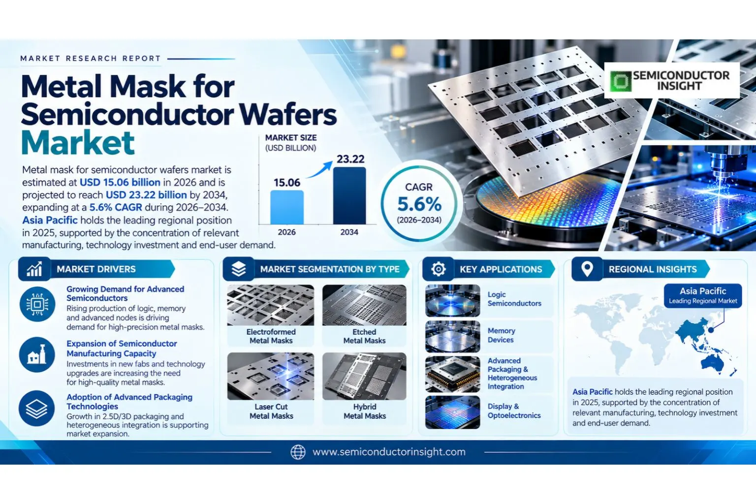
- Metal Mask for Semiconductor Wafers market is estimated at USD 15.06 billion in 2026 and is projected to reach USD 23.22 billion by 2034, representing a 5.6% CAGR over 2026–2034.
- Electroformed Metal Masks represents the largest type position, while Hybrid Metal Masks benefits most from the current shift toward higher-value and more integrated system architectures.
- Semiconductor Lithography is the largest application, while Wafer Level Packaging shows the strongest incremental opportunity as end users expand automation, precision control and data-rich monitoring.
- Asia Pacific holds the leading regional position in 2025 because its industrial base, customer concentration and technology ecosystem create the strongest commercial pull for suppliers.
- The main growth engine is growth in semiconductor and packaging output, whereas rising precision cost at fine geometries remains the most persistent constraint on broader adoption.
- Competitive advantage is shifting toward suppliers that combine core hardware performance with application software, qualification support, integration capability and regional service rather than competing on component specifications alone.
Metal Mask for Semiconductor Wafers Market Overview
Metal mask for semiconductor wafers market is estimated at USD 15.06 billion in 2026 and is projected to reach USD 23.22 billion by 2034, expanding at a 5.6% CAGR during 2026–2034. Asia Pacific holds the leading regional position in 2025, supported by the concentration of relevant manufacturing, technology investment and end-user demand.
Metal masks for semiconductor wafers are precision patterning and deposition tools used where apertures, openings or selective material transfer must be controlled across wafers, packages, MEMS structures, LEDs and display-related processes. The market includes electroformed, etched, laser-cut and hybrid masks, with performance governed by dimensional accuracy, flatness, material stability, defect control and usable lifetime. Demand is linked to semiconductor output but increasingly shaped by advanced packaging and heterogeneous integration, where tighter pitch and more complex package structures raise the value of high-precision masking and stencil technologies.
Mask economics are strongly influenced by yield rather than unit purchase price. A dimensionally unstable or contaminated mask can propagate defects across many wafers or panels, so advanced customers prioritize flatness, aperture uniformity, cleanability, lifetime and supplier process control. Electroforming supports fine, repeatable apertures, while etched and laser-cut designs remain attractive where cost, turnaround or geometry flexibility are more important. Hybrid structures can combine material and process advantages for demanding packaging or display applications.
The market should be understood as a system-level purchasing decision rather than a standalone component category. Buyers evaluate performance, qualification risk, integration time, service response and lifecycle cost together. This shifts value toward suppliers with proven application engineering and repeatable production capability. The result is a market in which technical differentiation can support pricing, but only when the supplier can translate specifications into measurable yield, uptime, safety, throughput or maintenance benefits for the end user.
Segment Analysis: By Type
By type, the Metal Mask for Semiconductor Wafers market is segmented into Electroformed Metal Masks, Etched Metal Masks, Laser Cut Metal Masks, Hybrid Metal Masks. Electroformed Metal Masks holds the leading position, while the fastest growth is concentrated in configurations that solve higher-value integration, reliability or performance requirements rather than purely price-driven use cases.
| Type | Market position and demand characteristics |
|---|---|
| Electroformed Metal Masks | Electroformed Metal Masks serves a distinct set of performance and cost requirements within the market. Its commercial position depends on application fit, technical qualification, integration complexity and the supplier’s ability to maintain repeatable performance across production environments. Largest type reflects the balance between installed-base demand and the rate at which customers are shifting toward more advanced configurations. |
| Etched Metal Masks | Etched Metal Masks serves a distinct set of performance and cost requirements within the market. Its commercial position depends on application fit, technical qualification, integration complexity and the supplier’s ability to maintain repeatable performance across production environments. Established segment reflects the balance between installed-base demand and the rate at which customers are shifting toward more advanced configurations. |
| Laser Cut Metal Masks | Laser Cut Metal Masks serves a distinct set of performance and cost requirements within the market. Its commercial position depends on application fit, technical qualification, integration complexity and the supplier’s ability to maintain repeatable performance across production environments. Established segment reflects the balance between installed-base demand and the rate at which customers are shifting toward more advanced configurations. |
| Hybrid Metal Masks | Hybrid Metal Masks serves a distinct set of performance and cost requirements within the market. Its commercial position depends on application fit, technical qualification, integration complexity and the supplier’s ability to maintain repeatable performance across production environments. Fastest-growing type reflects the balance between installed-base demand and the rate at which customers are shifting toward more advanced configurations. |
Type selection is increasingly driven by total system economics
Customers increasingly compare metal mask for semiconductor wafers configurations on total installed value rather than purchase price alone. A higher-cost solution can be preferred when it reduces calibration time, improves yield, eliminates auxiliary hardware or provides better diagnostic information. This favors products that simplify integration and support consistent operation at scale. Commodity configurations remain important for cost-sensitive applications, but margin and strategic differentiation are concentrated in products that solve a difficult measurement, automation or reliability problem.
Segment Analysis: By Application
By application, demand spans Wafer Level Packaging, Thin Film Deposition, Surface Mount Technology (SMT), Semiconductor Lithography, LED Packaging, OLED Display Manufacturing, Microelectromechanical Systems (MEMS), Others. Semiconductor Lithography forms the largest application base, while Wafer Level Packaging is positioned for the strongest incremental growth as customers increase investment in automation, precision and connected operations.
| Application | Demand characteristics |
|---|---|
| Wafer Level Packaging | Fastest-growing application. Purchasing is driven by the requirement to improve process control, reliability, safety or throughput in this application. Buyers typically qualify suppliers on performance under real operating conditions, integration with existing equipment and the economic cost of failure. Growth therefore depends on the pace of capital deployment and the degree to which the technology becomes embedded in standard equipment architectures. |
| Thin Film Deposition | Relevant demand segment. Purchasing is driven by the requirement to improve process control, reliability, safety or throughput in this application. Buyers typically qualify suppliers on performance under real operating conditions, integration with existing equipment and the economic cost of failure. Growth therefore depends on the pace of capital deployment and the degree to which the technology becomes embedded in standard equipment architectures. |
| Surface Mount Technology (SMT) | Relevant demand segment. Purchasing is driven by the requirement to improve process control, reliability, safety or throughput in this application. Buyers typically qualify suppliers on performance under real operating conditions, integration with existing equipment and the economic cost of failure. Growth therefore depends on the pace of capital deployment and the degree to which the technology becomes embedded in standard equipment architectures. |
| Semiconductor Lithography | Largest application. Purchasing is driven by the requirement to improve process control, reliability, safety or throughput in this application. Buyers typically qualify suppliers on performance under real operating conditions, integration with existing equipment and the economic cost of failure. Growth therefore depends on the pace of capital deployment and the degree to which the technology becomes embedded in standard equipment architectures. |
| LED Packaging | Relevant demand segment. Purchasing is driven by the requirement to improve process control, reliability, safety or throughput in this application. Buyers typically qualify suppliers on performance under real operating conditions, integration with existing equipment and the economic cost of failure. Growth therefore depends on the pace of capital deployment and the degree to which the technology becomes embedded in standard equipment architectures. |
| OLED Display Manufacturing | Relevant demand segment. Purchasing is driven by the requirement to improve process control, reliability, safety or throughput in this application. Buyers typically qualify suppliers on performance under real operating conditions, integration with existing equipment and the economic cost of failure. Growth therefore depends on the pace of capital deployment and the degree to which the technology becomes embedded in standard equipment architectures. |
| Microelectromechanical Systems (MEMS) | Relevant demand segment. Purchasing is driven by the requirement to improve process control, reliability, safety or throughput in this application. Buyers typically qualify suppliers on performance under real operating conditions, integration with existing equipment and the economic cost of failure. Growth therefore depends on the pace of capital deployment and the degree to which the technology becomes embedded in standard equipment architectures. |
| Others | Relevant demand segment. Purchasing is driven by the requirement to improve process control, reliability, safety or throughput in this application. Buyers typically qualify suppliers on performance under real operating conditions, integration with existing equipment and the economic cost of failure. Growth therefore depends on the pace of capital deployment and the degree to which the technology becomes embedded in standard equipment architectures. |
Additional Segment Analysis: By Size
| Size | Commercial relevance |
|---|---|
| 550×636 mm | This segment represents a distinct commercial configuration within the metal mask for semiconductor wafers market. Adoption depends on performance requirements, cost, compatibility with the host system and the level of qualification demanded by the target industry. Suppliers that can offer multiple configurations across the same platform improve cross-selling opportunities and reduce the customer’s engineering burden when moving between applications. |
| 550×550 mm | This segment represents a distinct commercial configuration within the metal mask for semiconductor wafers market. Adoption depends on performance requirements, cost, compatibility with the host system and the level of qualification demanded by the target industry. Suppliers that can offer multiple configurations across the same platform improve cross-selling opportunities and reduce the customer’s engineering burden when moving between applications. |
Additional Segment Analysis: By End User
| End User | Commercial relevance |
|---|---|
| Semiconductor Manufacturers | This segment represents a distinct commercial configuration within the metal mask for semiconductor wafers market. Adoption depends on performance requirements, cost, compatibility with the host system and the level of qualification demanded by the target industry. Suppliers that can offer multiple configurations across the same platform improve cross-selling opportunities and reduce the customer’s engineering burden when moving between applications. |
| Electronics Manufacturers | This segment represents a distinct commercial configuration within the metal mask for semiconductor wafers market. Adoption depends on performance requirements, cost, compatibility with the host system and the level of qualification demanded by the target industry. Suppliers that can offer multiple configurations across the same platform improve cross-selling opportunities and reduce the customer’s engineering burden when moving between applications. |
| Display Manufacturers | This segment represents a distinct commercial configuration within the metal mask for semiconductor wafers market. Adoption depends on performance requirements, cost, compatibility with the host system and the level of qualification demanded by the target industry. Suppliers that can offer multiple configurations across the same platform improve cross-selling opportunities and reduce the customer’s engineering burden when moving between applications. |
| MEMS Manufacturers | This segment represents a distinct commercial configuration within the metal mask for semiconductor wafers market. Adoption depends on performance requirements, cost, compatibility with the host system and the level of qualification demanded by the target industry. Suppliers that can offer multiple configurations across the same platform improve cross-selling opportunities and reduce the customer’s engineering burden when moving between applications. |
| Research and Development Institutes | This segment represents a distinct commercial configuration within the metal mask for semiconductor wafers market. Adoption depends on performance requirements, cost, compatibility with the host system and the level of qualification demanded by the target industry. Suppliers that can offer multiple configurations across the same platform improve cross-selling opportunities and reduce the customer’s engineering burden when moving between applications. |
Regional Analysis
Asia Pacific leads the Metal Mask for Semiconductor Wafers market in 2025, while regional growth rates differ according to manufacturing concentration, technology adoption, end-user investment and local supply-chain maturity. The market is not simply a set of geographic revenue pools; each region has a different purchasing logic and supplier-selection process.
How does regional demand differ across the Metal Mask for Semiconductor Wafers market?
Regional demand is shaped by where the relevant equipment is built, where end users deploy it, and how quickly local customers adopt advanced technologies. Mature regions tend to place greater weight on qualification, software and service, while high-growth manufacturing regions generate more unit demand and new design-in opportunities. Project-led regions can still be commercially attractive when applications are high value. Suppliers therefore need regional product positioning rather than a single global sales approach.
| Region | Position | Growth outlook | Demand profile | Supplier-selection gate |
|---|---|---|---|---|
| Asia Pacific | Largest | High | Manufacturing and technology-led | Local service, qualification and supply reliability |
| North America | High-value established | Moderate-high | Innovation and replacement-led | Local service, qualification and supply reliability |
| Europe | High-value established | Moderate-high | Engineering and regulation-led | Local service, qualification and supply reliability |
| South America | Emerging / project-led | Selective | Project-led | Local service, qualification and supply reliability |
| Middle East & Africa | Emerging / project-led | Selective | Project-led | Local service, qualification and supply reliability |
Key Metal Mask for Semiconductor Wafers Manufacturers and Competitive Landscape
Competition in the Metal Mask for Semiconductor Wafers market is shaped by application expertise, product reliability, integration capability and global support. The market includes established multinational suppliers, specialist technology companies and regional competitors, with customer qualification creating meaningful switching costs in demanding applications.
Leading suppliers compete by building platforms that can be adapted across multiple customer requirements without forcing a complete redesign. This lowers development time for the customer and creates cross-selling opportunities for the vendor. Brand reputation matters most in high-cost or safety-critical applications, where the financial impact of unreliable measurement or control can exceed the purchase price of the hardware by a wide margin.
Specialist companies remain important because many applications require niche performance, custom packaging or proprietary algorithms. These firms can win against larger suppliers when they solve a difficult technical problem faster or provide more responsive engineering support. However, scaling from prototype to volume production requires quality systems, manufacturing repeatability and a service model that can support customers in multiple regions.
Regional competitors often enter through cost-sensitive applications and then move upward as product quality improves. Their strongest advantage is usually local access, shorter lead time and willingness to customize. Global suppliers respond by broadening product families and adding software, diagnostics and support services that make direct price comparison more difficult. The result is a tiered market rather than a single winner-takes-all structure.
| Competitive tier | Representative companies | Typical advantage |
|---|---|---|
| Global technology leaders | Toppan, Dai Nippon Printing (DNP), Maxell, Athene, HOYA | Broad portfolios, strong qualification history, global support and premium applications |
| Established specialists | SK-Electronics, ShenZheng QingVi, Nippon Filcon, Newway Photomask, PHOTOMASK PORTAL | Focused technical niches, application depth and regional strengths |
| Emerging / niche suppliers | Customization, local access and targeted product differentiation |
Companies profiled
The profiled supplier set includes Toppan, Dai Nippon Printing (DNP), Maxell, Athene, HOYA, SK-Electronics, ShenZheng QingVi, Nippon Filcon, Newway Photomask, PHOTOMASK PORTAL. The competitive relevance of each company varies by geography, product architecture and target application, so customer shortlists are usually narrower than the complete profiled universe.
Metal Mask for Semiconductor Wafers Production Capacity Analysis
Production capacity for Metal Mask for Semiconductor Wafers products is concentrated where the enabling components, precision manufacturing skills and end-user industries are already established. Capacity expansion therefore follows both customer proximity and access to specialized process know-how.
The production footprint is constrained by more than factory floor space. Critical inputs can include precision materials, semiconductor or optical components, calibration equipment, clean manufacturing, specialized test systems and engineering labor. Capacity that lacks validated quality systems is not interchangeable with qualified capacity, particularly in semiconductor, automotive, medical or aerospace applications. As a result, suppliers often scale through phased line additions and customer qualification rather than by building large speculative capacity.
Asia Pacific has the strongest manufacturing density for many electronic and precision components, while North America and Europe retain substantial high-value engineering and specialty production. Regional diversification is increasing as customers seek supply resilience, but duplicating advanced production requires process transfer, trained staff and long qualification cycles. The practical supply risk is therefore concentrated in specialized subcomponents and manufacturing know-how rather than in basic assembly alone.
Metal Mask for Semiconductor Wafers Market Dynamics: Drivers, Restraints and Opportunities
The market outlook combines structural growth from growth in semiconductor and packaging output with persistent constraints from rising precision cost at fine geometries. The strongest suppliers will be those that convert technical performance into lower total cost, better uptime, improved yield or new end-user functionality.
MARKET DRIVERS
| Driver | Impact | Commercial mechanism |
|---|---|---|
| Growth in semiconductor and packaging output | High | More wafer starts and packaging steps directly increase demand for precision masks used in deposition, pattern transfer and assembly. SEMI reported record semiconductor materials r… |
| Advanced packaging complexity | High | Chiplets, fan-out packaging, wafer-level packaging and high-density interconnects increase the number of fine-pitch material-deposition and patterning operations. As bump and inter… |
| Higher lithography and patterning precision | Medium-High | Semiconductor scaling and more complex device structures create tighter tolerance requirements across multiple process steps. Even where optical photomasks dominate front-end litho… |
| Regional expansion of wafer fabs | Medium | SEMI reported a geographically diverse pipeline of new fabs and continued 300 mm capacity expansion. New production lines create demand for supporting patterning, deposition and pa… |
Growth in semiconductor and packaging output
More wafer starts and packaging steps directly increase demand for precision masks used in deposition, pattern transfer and assembly. SEMI reported record semiconductor materials revenue of $73.2 billion in 2025, with both wafer-fab and packaging materials growing. The same increase in process activity supports consumables and tooling such as masks, especially where each product generation requires new patterns and tighter dimensional control.
Advanced packaging complexity
Chiplets, fan-out packaging, wafer-level packaging and high-density interconnects increase the number of fine-pitch material-deposition and patterning operations. As bump and interconnect dimensions shrink, mask flatness and aperture repeatability become more important to paste, metal or film transfer. Advanced packaging therefore raises both the volume and value of mask requirements relative to mature, lower-density assembly.
Higher lithography and patterning precision
Semiconductor scaling and more complex device structures create tighter tolerance requirements across multiple process steps. Even where optical photomasks dominate front-end lithography, metal masks remain relevant in specialty deposition, MEMS, packaging and display processes. Suppliers capable of finer features, lower distortion and better defect control can participate in higher-value applications as customers reduce allowable process variation.
Regional expansion of wafer fabs
SEMI reported a geographically diverse pipeline of new fabs and continued 300 mm capacity expansion. New production lines create demand for supporting patterning, deposition and packaging tooling, while local supply-chain resilience becomes more important. Mask suppliers with manufacturing or service close to Asian and emerging regional semiconductor clusters can reduce lead times for custom designs and replacements.
MARKET RESTRAINTS
| Restraint | Impact | Commercial mechanism |
|---|---|---|
| Rising precision cost at fine geometries | High | Producing fine apertures with tight dimensional control raises tooling, inspection and process-control cost. Yield losses during mask fabrication can be significant because a small… |
| Competition from alternative patterning methods | Medium-High | Direct-write lithography, photoresist-based processes, alternative stencil materials and other deposition techniques can replace metal masks in selected process flows. Customers co… |
| Mask wear, cleaning and distortion | Medium | Masks are consumable tools exposed to repeated handling, cleaning, temperature cycles and deposited material. Aperture clogging, mechanical damage or loss of tension can degrade tr… |
| Long qualification cycles | Medium | A mask design is tied to a specific process recipe, material stack and product geometry. Changes can require new dimensional qualification, pilot production and defect validation b… |
Rising precision cost at fine geometries
Producing fine apertures with tight dimensional control raises tooling, inspection and process-control cost. Yield losses during mask fabrication can be significant because a small defect may make an entire high-value mask unusable. As feature requirements tighten, suppliers must invest in cleaner production, better inspection and more stable materials, increasing capital intensity and limiting the number of vendors able to serve advanced applications.
Competition from alternative patterning methods
Direct-write lithography, photoresist-based processes, alternative stencil materials and other deposition techniques can replace metal masks in selected process flows. Customers compare total process cost, resolution, throughput and contamination risk. Metal masks remain attractive where they provide simple, repeatable transfer, but the addressable market is constrained when a non-contact or maskless approach offers better scaling.
Mask wear, cleaning and distortion
Masks are consumable tools exposed to repeated handling, cleaning, temperature cycles and deposited material. Aperture clogging, mechanical damage or loss of tension can degrade transfer quality and force replacement. End users therefore evaluate lifetime and cleanability carefully, and suppliers must design for both dimensional precision and robust maintenance. Frequent replacement can raise ownership cost and slow adoption in cost-sensitive applications.
Long qualification cycles
A mask design is tied to a specific process recipe, material stack and product geometry. Changes can require new dimensional qualification, pilot production and defect validation before high-volume use. This creates switching costs that protect qualified incumbents but can also lengthen the sales cycle for new suppliers and reduce the pace at which innovative mask designs move into mass production.
MARKET OPPORTUNITIES
Advanced packaging and chiplets
Wafer-level packaging, fan-out structures and chiplet integration increase demand for high-precision deposition and interconnect formation. Mask suppliers can create specialized products for fine-pitch bumps, redistribution layers and package-level material transfer. The opportunity is strongest where the supplier can co-develop mask geometry with process engineers and shorten iteration cycles during package qualification.
Display, microLED and specialty electronics
Fine metal masks have established roles in OLED and can support other specialty deposition processes where patterned material transfer is required. Emerging microLED, sensor and photonics applications can create additional custom mask demand. These markets favor suppliers that can handle larger formats, tight tension control and frequent design changes rather than only standardized semiconductor geometries.
Southeast Asian manufacturing expansion
Malaysia, Vietnam and other Southeast Asian locations are attracting semiconductor packaging, testing and electronics investments. A growing local customer base creates opportunities for regional mask production, repair and rapid-turn engineering support. Because custom masks are time-sensitive tools, local service can be a meaningful differentiator against long international lead times.
Materials and surface engineering
New nickel alloys, molybdenum-based structures, coatings and hybrid mask constructions can improve lifetime, thermal stability or release behavior. Suppliers that combine precision fabrication with materials engineering can reduce defect rates and extend cleaning cycles, giving customers a measurable cost-per-wafer benefit and supporting premium pricing.
Metal Mask for Semiconductor Wafers Supply Chain Analysis
Raw materials & enabling components
Core manufacturing
Integration & distribution
End-use operation
Raw materials & enabling components
Specialized materials, semiconductor devices, optics, mechanics, RF parts or precision substrates depending on architecture. Value capture rises when a supplier controls a difficult-to-replicate capability such as proprietary design, precision calibration, qualification data or software integration. Bottlenecks become commercially important when they lengthen lead times or limit the ability to qualify alternative suppliers, which is why customers increasingly evaluate resilience as part of sourcing decisions.
Core manufacturing
Fabrication, assembly, calibration, software loading and quality control that establish product performance and repeatability. Value capture rises when a supplier controls a difficult-to-replicate capability such as proprietary design, precision calibration, qualification data or software integration. Bottlenecks become commercially important when they lengthen lead times or limit the ability to qualify alternative suppliers, which is why customers increasingly evaluate resilience as part of sourcing decisions.
Integration & distribution
OEM design-in, distributors, system integrators and applications teams that adapt the product to customer equipment. Value capture rises when a supplier controls a difficult-to-replicate capability such as proprietary design, precision calibration, qualification data or software integration. Bottlenecks become commercially important when they lengthen lead times or limit the ability to qualify alternative suppliers, which is why customers increasingly evaluate resilience as part of sourcing decisions.
End-use operation
Factories, vehicles, research laboratories, infrastructure or industrial assets where recurring replacement and service demand is created. Value capture rises when a supplier controls a difficult-to-replicate capability such as proprietary design, precision calibration, qualification data or software integration. Bottlenecks become commercially important when they lengthen lead times or limit the ability to qualify alternative suppliers, which is why customers increasingly evaluate resilience as part of sourcing decisions.
Recent Developments in the Metal Mask for Semiconductor Wafers Market
SEMI reported that semiconductor materials revenue reached a record $73.2 billion in 2025, including $45.8 billion in wafer-fabrication materials and $27.4 billion in packaging materials. The result indicates higher process activity in both front-end and packaging operations, supporting demand for precision masks, stencils and related pattern-transfer consumables used in advanced manufacturing.
SEMI’s latest photomask characterization framework continues to track merchant and captive photomask demand across North America, Japan, Europe, Taiwan, Korea, China and the rest of the world, including technology trends beyond 3 nm. The regional and technology coverage underscores the importance of supplier capability, geometry scaling and local manufacturing relationships in the broader mask ecosystem.
SEMI identified 18 semiconductor fab construction projects expected to start in 2025, including fifteen 300 mm facilities. New fabs increase the downstream need for qualified process tooling and consumables while broadening demand geographically, particularly in regions seeking more resilient local semiconductor supply chains.
REPORT SCOPE & SEGMENTATION
| Attribute | Coverage |
|---|---|
| Base Year | 2025 |
| Estimated Year | 2026 |
| Forecast Period | 2026–2034 |
| 2025 Market Size | USD 14.26 billion |
| 2026 Market Size | USD 15.06 billion |
| 2034 Projected Market Size | USD 23.22 billion |
| CAGR (2026–2034) | 5.6% |
| Largest Market in 2025 | Asia Pacific |
| By Type | Electroformed Metal Masks, Etched Metal Masks, Laser Cut Metal Masks, Hybrid Metal Masks |
| By Application | Wafer Level Packaging, Thin Film Deposition, Surface Mount Technology (SMT), Semiconductor Lithography, LED Packaging, OLED Display Manufacturing, Microelectromechanical Systems (MEMS), Others |
| By Size | 550×636 mm, 550×550 mm |
| By End User | Semiconductor Manufacturers, Electronics Manufacturers, Display Manufacturers, MEMS Manufacturers, Research and Development Institutes |
| Regions | North America; Europe; Asia Pacific; South America; Middle East & Africa |
| Companies Profiled | Toppan, Dai Nippon Printing (DNP), Maxell, Athene, HOYA, SK-Electronics, ShenZheng QingVi, Nippon Filcon, Newway Photomask, PHOTOMASK PORTAL |
Frequently Asked Questions
What is the current size of the Metal Mask for Semiconductor Wafers market?
The global Metal Mask for Semiconductor Wafers market is estimated at USD 15.06 billion in 2026 and is projected to reach USD 23.22 billion by 2034, representing a 5.6% CAGR during 2026–2034. The 2025 base-year market size is USD 14.26 billion. Growth is supported by higher end-user technology intensity, automation and the need for more reliable or precise system performance.
Which region leads the Metal Mask for Semiconductor Wafers market?
Asia Pacific holds the leading regional position in 2025. Its advantage reflects the concentration of relevant manufacturing, technology investment and end-user activity. Other regions remain commercially important for premium applications, research, regulation-driven adoption or project demand, so suppliers typically use different channel and service strategies by geography.
Which type leads the Metal Mask for Semiconductor Wafers market?
Electroformed Metal Masks holds the strongest current type position. Its leadership is tied to broad application coverage, installed-base demand and a favorable balance between performance and cost. Growth within the type segment increasingly depends on automation, digital integration and the ability to reduce total system cost rather than on standalone hardware specifications.
Which application is the largest for Metal Mask for Semiconductor Wafers?
Semiconductor Lithography forms the largest application base, reflecting the technology’s established role in processes where accuracy, control, reliability or sensing quality directly affects output. Wafer Level Packaging offers a strong incremental opportunity as investment shifts toward more automated, data-rich and performance-sensitive operating environments.
What are the main growth drivers?
The main growth drivers are growth in semiconductor and packaging output, advanced packaging complexity, higher lithography and patterning precision and regional expansion of wafer fabs. Together they increase either the number of addressable system installations or the value of technology required per installation, supporting both unit demand and higher-value product configurations.
What are the main restraints on market growth?
Growth is constrained by rising precision cost at fine geometries, competition from alternative patterning methods, mask wear, cleaning and distortion and long qualification cycles. These factors affect adoption economics, qualification timing or competitive substitution. Suppliers mitigate them through integration, automation, software, service and more application-specific product design.
Who are the key companies in the Metal Mask for Semiconductor Wafers market?
Key companies profiled include Toppan, Dai Nippon Printing (DNP), Maxell, Athene, HOYA, SK-Electronics, ShenZheng QingVi, Nippon Filcon, together with additional specialist and regional suppliers. Competitive position varies by product architecture, geography and application. Customers usually shortlist suppliers based on qualification history, performance, integration capability and local support rather than company size alone.
Which technology trends are shaping the market?
The most important technology trends are greater automation, digital connectivity, embedded diagnostics, software-assisted analysis and tighter integration with the host system. These changes move the product from a passive hardware component toward a more intelligent subsystem. Suppliers that can verify performance under production conditions are better positioned to defend pricing and secure long-term design wins.
Where are the strongest new opportunities?
New opportunities are concentrated in advanced packaging and chiplets, display, microled and specialty electronics, southeast asian manufacturing expansion and materials and surface engineering. The common theme is that customers are willing to adopt higher-value technology when it enables a new function, reduces maintenance or improves operating economics in a measurable way.
What is the outlook for the Metal Mask for Semiconductor Wafers market through 2034?
The market is projected to reach USD 23.22 billion by 2034 from USD 15.06 billion in 2026, a 5.6% CAGR. Growth should remain uneven by segment and region, with the best performance coming from applications where the technology becomes embedded in new equipment architectures, automation programs or high-value measurement and control workflows.
Research Sources & Evidence Base
View research sources used for this overview.
- SEMI. Photomask Market Characterization Report. Supporting evidence for industry activity, technology development, regional demand or competitive context.
- SEMI. Global Semiconductor Materials Market Revenue Reaches Record $73.2 Billion in 2025. Supporting evidence for industry activity, technology development, regional demand or competitive context.
- SEMI. Eighteen New Semiconductor Fabs to Start Construction in 2025. Supporting evidence for industry activity, technology development, regional demand or competitive context.
- SEMI. 300mm Fab Outlook. Supporting evidence for industry activity, technology development, regional demand or competitive context.
Get Sample Report PDF for Exclusive Insights
Report Sample Includes
- Table of Contents
- List of Tables & Figures
- Charts, Research Methodology, and more...
 Download Sample Report PDF