Photomask Market, Emerging Trends, Technological Advancements, and Business Strategies 2025-2032

Photomask Market size was valued at USD 5.53 billion in 2024 to USD 7.68 billion by 2032, exhibiting a CAGR of 4.9% during the forecast period

PDF Icon Download Sample Report PDF
  • Quick Dispatch

    All Orders

  • Secure Payment

    100% Secure Payment

Price range: $1,500.00 through $4,250.00

Clear

MARKET INSIGHTS

Global Photomask Market size was valued at USD 5.53 billion in 2024 to USD 7.68 billion by 2032, exhibiting a CAGR of 4.9% during the forecast period.

Photomasks are high-precision quartz or glass plates containing microscopic patterns of integrated circuits (ICs). They are fundamental components in the photolithography process, acting as a stencil to transfer complex circuit designs onto semiconductor wafers.

The market growth is primarily driven by the relentless demand for advanced electronics and the continuous miniaturization of semiconductor components. The transition to Extreme Ultraviolet (EUV) lithography represents a major driver, as EUV masks enable the creation of significantly smaller features on chips. Furthermore, the expansion of memory technologies like 3D NAND, which requires a high volume of photomasks, further propels the industry forward. Key players are actively investing in new technologies and forming strategic collaborations to meet evolving demands; for instance, industry leaders are expanding production capacity for EUV masks to support next-generation chip manufacturing. Photronics Inc., Toppan Printing Co., Ltd., and DNP are some of the key players that operate in the market with a wide range of portfolios.
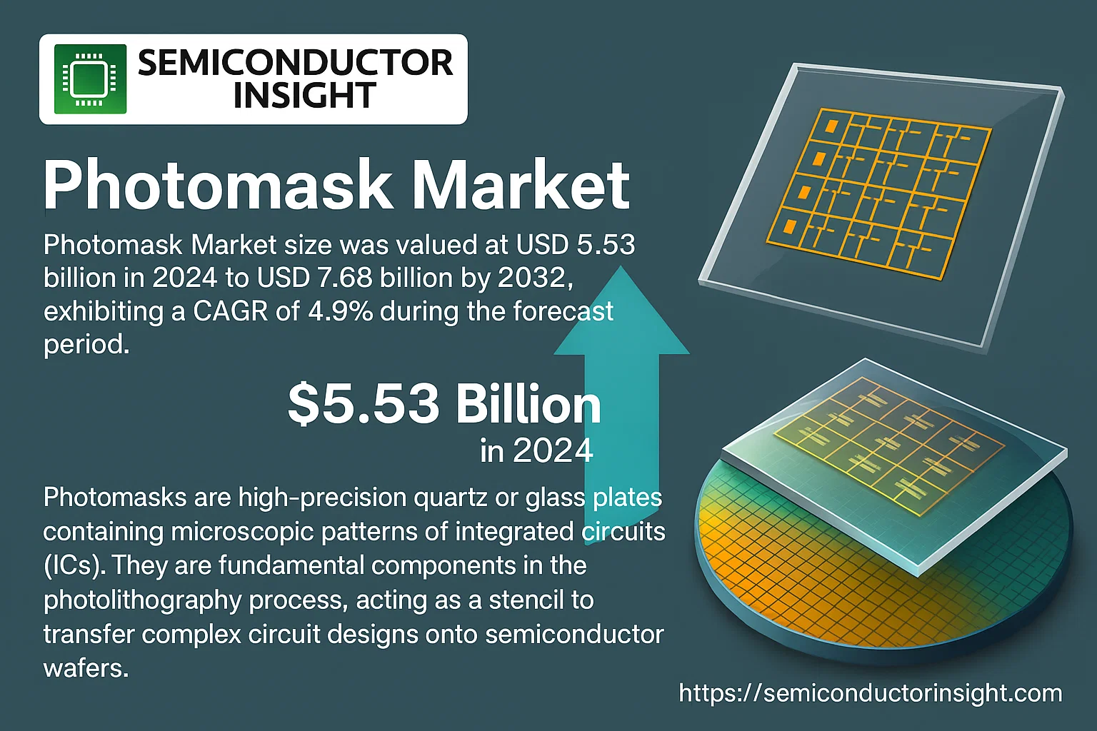
Photomask Market Share-semiconductorinsight

MARKET DRIVERS

Proliferation of Advanced Semiconductor Nodes

The relentless demand for smaller, faster, and more power-efficient electronic devices is a primary driver. This fuels the transition to advanced technology nodes below 7nm and 5nm, which require extremely sophisticated and precise photomasks. The need for multi-patterning techniques like EUV lithography has significantly increased the volume and complexity of photomasks used per chip design.

Expansion of the Consumer Electronics and Automotive Sectors

Growth in markets such as smartphones, high-performance computing, and the integration of advanced electronics in automotive applications, including electric vehicles and ADAS, creates sustained demand for the semiconductors that depend on photomasks. The increasing semiconductor content per vehicle and the rollout of 5G infrastructure are providing robust, long-term demand signals for the photomask industry.

Global push for digital transformation across industries is accelerating the adoption of ICs, directly impacting photomask consumption.

Furthermore, investments in new semiconductor fabrication facilities (fabs) worldwide, particularly for leading-edge logic and memory chips, ensure a steady pipeline of demand for high-quality photomasks from specialized merchant mask shops and captive mask operations.

MARKET CHALLENGES

Exponentially Rising Costs and Complexity

As feature sizes shrink to atomic levels, the cost and technical complexity of photomask manufacturing skyrocket. The shift to EUV lithography requires entirely new mask infrastructure, including defect-free multilayer blanks and highly specialized pellicles. The capital expenditure for an advanced mask shop can exceed hundreds of millions of dollars, creating a high barrier to entry.

Other Challenges

Cycle Time and Turnaround Pressure
The increasing design complexity of integrated circuits extends the data preparation and mask writing time. Meeting the aggressive time-to-market demands of semiconductor companies while ensuring zero-defect masks presents a significant operational challenge for mask manufacturers.

Supply Chain and Material Availability
The industry faces challenges related to the supply of critical raw materials, such as high-purity quartz substrates and specialized chemicals. Geopolitical tensions and trade restrictions can disrupt the supply chain for these essential components, impacting production schedules.

MARKET RESTRAINTS

High Capital Investment and Consolidation

The immense capital required for R&D and next-generation manufacturing equipment acts as a major restraint. This has led to significant consolidation within the merchant Photomask Market, with only a handful of large, globally capable players able to afford the investments needed for leading-edge technology. This limits competition and can concentrate pricing power.

Technical Limitations and Yield Management

Pushing the boundaries of physics introduces formidable technical restraints, particularly in defect control. A single, minute defect on a photomask can ruin an entire wafer, leading to substantial financial losses. Maintaining high yields for increasingly complex masks, especially for EUV, remains a persistent challenge that restrains rapid scalability.

MARKET OPPORTUNITIES

Adoption of Extreme Ultraviolet (EUV) Lithography

The mainstream adoption of EUV lithography for high-volume manufacturing at nodes of 7nm and below represents the single largest opportunity. This creates demand for a new generation of EUV masks, along with associated services like mask blank production, inspection, repair, and pellicle integration, opening new revenue streams for technology leaders.

Emerging Applications in Advanced Packaging

Beyond traditional front-end scaling, advanced packaging technologies like Fan-Out Wafer-Level Packaging (FOWLP) and 3D IC stacking require specialized photomasks. The growth in heterogeneous integration provides a significant opportunity for mask makers to serve a diversifying market that is less dependent on the most aggressive lithography nodes.

AI and Machine Learning for Mask Optimization

The application of artificial intelligence and machine learning in computational lithography and mask data preparation offers substantial opportunities to improve design accuracy, reduce turnaround times, and enhance defect prediction. Companies that develop and integrate these smart manufacturing solutions can gain a competitive advantage.

Photomask Market Trends
Advanced Lithography and Material Innovations Dominate

Global Photomask Market is propelled by the demand for smaller, more powerful semiconductor devices. Valued at USD 5.53 billion in 2024, the market is projected to grow at a CAGR of 4.9% to reach USD 7.68 billion by 2032. A primary driver is the critical transition to Extreme Ultraviolet (EUV) lithography. As semiconductor nodes shrink to 5nm and beyond, EUV lithography’s extremely short wavelength is essential for patterning features that are impossible with traditional methods. This shift necessitates the development of specialized EUV photomasks, which are constructed with new materials and manufacturing techniques to handle the high-energy light source, representing a significant technological and market trend.

Other Trends

Multiple Patterning Techniques

To overcome the limitations of optical lithography at advanced nodes, multiple patterning techniques like double and quadruple patterning have become standard. These processes require multiple, highly precise photomasks to create a single circuit layer, thereby increasing the volume and complexity of masks needed per wafer. This trend directly supports market growth by escalating the demand for advanced photomasks, even as feature sizes become smaller than the wavelength of light used to print them.

Supply Chain and Market Consolidation

The Photomask Market is characterized by a concentrated competitive landscape, with the top 10 players accounting for approximately 52% of global revenue. High development costs for next-generation masks, such as those for EUV, are driving collaboration between manufacturers, semiconductor companies, and equipment suppliers. There is a parallel trend toward strengthening Global supply chain to mitigate risks from trade tensions and demand spikes, ensuring a stable supply of these critical components for semiconductor fabs worldwide.

Inspection and Automation Advancements

As photomask features shrink to the nanometer scale, the impact of even the smallest defect becomes catastrophic for chip yields. This has spurred the development of highly advanced inspection technologies capable of detecting sub-nanometer imperfections. Concurrently, the industry is increasingly adopting automation and sophisticated software for design, simulation, and process control. These tools optimize the mask-making workflow, reduce time-to-market for new semiconductor products, and enhance overall manufacturing yield, making them essential for remaining competitive in this high-stakes market.

COMPETITIVE LANDSCAPE

Key Industry Players

A Market Characterized by a Consolidated Top Tier and Specialized Niche Participants

Global Photomask Market exhibits a moderately consolidated structure, dominated by a handful of established global leaders. In 2023, the top 10 players collectively held approximately 52% of the market revenue, underscoring the significant market share concentration among key manufacturers. Companies like Photronics, Toppan Printing (Toppan), and Dai Nippon Printing (DNP) are the market frontrunners, leveraging their extensive technological expertise, global manufacturing footprints, and long-standing relationships with major semiconductor foundries and integrated device manufacturers (IDMs). This leadership is reinforced by their capacity to produce advanced photomasks, including those required for extreme ultraviolet (EUV) lithography and complex multiple patterning techniques, which are critical for manufacturing the most advanced semiconductor nodes. The high R&D and capital expenditure required to keep pace with semiconductor miniaturization trends act as significant barriers to entry, thereby solidifying the position of these incumbent leaders.

Beyond the dominant players, the market includes several other significant manufacturers that compete effectively in specific segments or geographic regions. Companies such as Hoya Corporation, a major supplier of photomask blanks, and SK-Electronics hold important positions in the supply chain. Regional specialists like Taiwan Mask Corporation (TMC) and Nippon Filcon serve crucial roles in key semiconductor manufacturing hubs in Asia. Furthermore, players like LG Innotek, ShenZheng QingVi, and Compugraphics International cater to diverse applications including flat panel displays (FPDs), touch panels, and printed circuit boards (PCBs), representing the market’s fragmentation in applications outside of the most advanced logic and memory chips. This dual structure of global giants and specialized regional or application-focused suppliers creates a dynamic competitive environment.

List of Key Photomask Companies Profiled

Segment Analysis:

Segment Category Sub-Segments Key Insights
By Type
  • Quartz Base Photomask
  • Soda Lime Base Photomask
  • Others
Quartz Base Photomask is the leading segment due to its superior performance characteristics essential for advanced semiconductor manufacturing. Its high thermal stability and optical transparency make it the preferred substrate for producing complex integrated circuits at leading-edge process nodes. The demand for quartz masks is strongly driven by the transition to Extreme Ultraviolet (EUV) lithography, which requires exceptionally durable and precise materials. As semiconductor features continue to shrink, the technical requirements for defect-free patterns intensify, further cementing the dominance of quartz-based solutions over alternatives like soda lime, which are typically reserved for less demanding applications.
By Application
  • Semiconductor Chip
  • Flat Panel Display
  • Touch Industry
  • Circuit Board
Semiconductor Chip manufacturing stands as the dominant application segment, consuming the most advanced and highest-value photomasks. This leadership is underpinned by the relentless demand for more powerful and energy-efficient microprocessors, memory chips, and sensors. The complexity of modern chip designs, which utilize multiple patterning and EUV lithography techniques, requires a significant number of sophisticated photomasks per wafer. While other applications like flat panel displays and circuit boards represent substantial markets, the technical challenges and innovation pace within semiconductor fabrication create a continuous, high-value demand that drives the overall Photomask Market forward.
By End User
  • Integrated Device Manufacturers (IDMs)
  • Foundries
  • Fabless Semiconductor Companies
Foundries represent the leading end-user segment, acting as the primary volume drivers for advanced photomask production. These specialized semiconductor manufacturing facilities serve a wide array of fabless companies and other clients, necessitating a diverse and extensive inventory of masks for various process technologies. The competitive nature of the foundry business, where technological leadership and production capacity are key differentiators, fuels continuous investment in the latest lithography equipment and the corresponding photomasks. This dynamic creates a highly demanding and innovation-focused customer base that consistently pushes the boundaries of photomask technology.
By Technology Node
  • Advanced Nodes (e.g., sub-10nm, EUV)
  • Mature Nodes (e.g., 28nm and above)
  • Legacy Nodes
Advanced Nodes are the primary growth engine for the Photomask Market, despite representing a smaller volume compared to mature nodes. The development and production of masks for sub-10nmprocess nodes and EUV lithography involve extreme technical complexity, requiring advanced materials like phase-shift masks and sophisticated inspection tools to detect nanometer-scale defects. This segment commands significantly higher prices per mask due to the intensive R&D, specialized equipment, and lower yields involved. The demand is driven by high-performance computing, AI accelerators, and leading-edge smartphone processors, creating a critical and high-value segment that defines the technological frontier of the industry.
By Mask Operation
  • Master Masks
  • Reticles
  • Multi-layer/Multi-patterning Sets
Multi-layer/Multi-patterning Sets have emerged as the leading segment in terms of strategic importance and complexity. As semiconductor manufacturing moves beyond the physical limits of single-exposure lithography, techniques like double and quadruple patterning have become standard for advanced nodes. This shift drastically increases the number of photomasks required to produce a single chip layer, creating demand for coordinated sets of masks. This trend elevates the importance of precision and defect control across an entire mask set, making the segment highly demanding and driving advancements in design-for-manufacturing software and automated inspection to ensure yield.

Regional Analysis: Photomask Market

Asia-Pacific

Asia-Pacific stands as the undisputed leader in Global Photomask Market, driven by its position as the world’s semiconductor manufacturing hub. The region benefits from an unparalleled concentration of major foundries, integrated device manufacturers, and display panel producers, which creates consistent and high-volume demand for advanced photomasks. Countries like Taiwan, South Korea, Japan, and China are at the forefront, with substantial investments in new fabrication facilities and research into next-generation nodes. The strong supporting ecosystem includes leading photomask manufacturers and material suppliers located in close proximity to their customers, facilitating tight collaboration essential for developing complex mask solutions for cutting-edge logic and memory chips. Government initiatives aimed at achieving technological self-sufficiency, particularly in China, are further accelerating the adoption of domestic semiconductor supply chains, thereby fueling the regional photomask industry. This symbiotic relationship between semiconductor production and photomask supply ensures the Asia-Pacific region’s continued dominance, supported by a highly skilled technical workforce and robust infrastructure for high-volume manufacturing.

Semiconductor Manufacturing Hub
The region’s dominance is rooted in its concentration of the world’s leading semiconductor foundries and memory chip makers. This creates a captive, high-demand market for photomasks required for advanced process nodes below 10nm. The proximity of mask shops to fabs enables rapid iteration and close technical collaboration, which is critical for yield enhancement and time-to-market for new chip designs, securing the region’s leadership.
Display Industry Strength
Beyond semiconductors, Asia-Pacific is Global center for display panel production, including LCD and advanced OLED technologies. This sector requires a significant volume of large-format photomasks for transistor array and color filter patterning. The continuous innovation and capacity expansion in displays, particularly for high-resolution screens and flexible panels, provides a substantial and stable secondary demand driver for the regional Photomask Market.
Government and Investment Support
Substantial government-backed initiatives and incentives, especially in China, South Korea, and Taiwan, are aggressively promoting domestic semiconductor and display industries. These policies aim to reduce dependency on foreign technology and build self-sufficient supply chains. This results in massive capital expenditure for new fabs and R&D centers, directly increasing the need for sophisticated, locally sourced photomasks and stimulating the entire regional market ecosystem.
Advanced Technology Adoption
Asia-Pacific leads the adoption of the most advanced patterning technologies, such as Extreme Ultraviolet (EUV) lithography, which requires highly complex and expensive EUV masks. The region’s major players are consistently first to deploy these next-generation tools, driving demand for the highest-value segment of the Photomask Market. This early and aggressive adoption cements the region’s role as the innovation and volume leader for cutting-edge photomask solutions.

North America
North America maintains a strong presence in the Photomask Market, characterized by a focus on high-value, leading-edge research, design, and low-volume, high-complexity production. The region is home to major fabless semiconductor companies and integrated device manufacturers that design the world’s most advanced chips. This drives demand for highly sophisticated photomasks, particularly for prototype development and specialized applications. While large-scale manufacturing has shifted to Asia, North America retains critical expertise in developing masks for emerging technologies, such as those for advanced microprocessors, AI accelerators, and specialized memory architectures. The market is supported by a robust ecosystem of specialized photomask vendors and strong R&D collaborations with national laboratories and universities, focusing on next-generation lithography and mask technologies.

Europe
Europe’s Photomask Market is defined by its specialization in niche, high-reliability applications, particularly for the automotive, industrial, and aerospace sectors. The region has a strong base of manufacturers requiring photomasks for specialized microcontrollers, power semiconductors, and sensors that demand extreme quality and longevity. While not a volume leader, Europe excels in producing masks for technologies like MEMS and power electronics, where precision and reliability are paramount. Collaborative research initiatives, such as those supported by the European Union, foster innovation in advanced packaging and More-than-Moore technologies, creating demand for specialized mask solutions. The presence of leading equipment suppliers for lithography tools also creates a synergistic environment for developing advanced mask-making processes.

South America
The Photomask Market in South America is relatively nascent and limited in scale compared to other regions. It is primarily driven by domestic demand for electronics assembly and a small but growing local semiconductor design industry, mainly in countries like Brazil. The market largely depends on imports for advanced photomasks, with local capabilities focused on supporting simpler, mature technology nodes for consumer electronics and industrial applications. There is limited indigenous manufacturing of high-end semiconductors, which constrains the growth of a sophisticated local photomask industry. However, initiatives to develop local technology hubs and increase regional technological independence could potentially stimulate future demand for basic photomask services.

Middle East & Africa
The Photomask Market in the Middle East & Africa region is the smallest globally, with very limited local semiconductor or display fabrication. Demand is almost entirely import-driven, serving small-scale electronics assembly and maintenance. A few initiatives, particularly in the Gulf Cooperation Council (GCC) countries, aim to diversify their economies into technology, but these are in early stages and have not yet translated into significant photomask demand. The market is characterized by a reliance on foreign suppliers for any advanced technology needs, with no substantial local photomask production infrastructure. Growth is expected to remain slow, tied to the broader and gradual development of the regional electronics manufacturing base.

Report Scope

This market research report provides a comprehensive analysis of the Photomask Market , covering the forecast period 2025–2032. It offers detailed insights into market dynamics, technological advancements, competitive landscape, and key trends shaping the industry.

Key focus areas of the report include:

  • Market Overview: The report begins with an overview outlining its current market scenario, key growth indicators, and industry transformation drivers. It discusses macroeconomic factors, demand–supply balance, regulatory landscape, and the strategic role of semiconductors in powering advancements across industries such as automotive, telecommunications, consumer electronics, and industrial automation.
  • Market Size & Forecast: Historical data and future projections for revenue, unit shipments, and market value across major regions and segments.
  • Segmentation Analysis: Detailed breakdown by product type, technology, application, and end-user industry to identify high-growth segments and investment opportunities.
  • Regional Insights: Insights into market performance across North America, Europe, Asia-Pacific, Latin America, and the Middle East & Africa, including country-level analysis where relevant.
  • Competitive Landscape: Profiles of leading market participants, including their product offerings, R&D focus, manufacturing capacity, pricing strategies, and recent developments such as mergers, acquisitions, and partnerships.
  • Technology Trends & Innovation: Assessment of emerging technologies, integration of AI/IoT, semiconductor design trends, fabrication techniques, and evolving industry standards.
  • Market Drivers & Restraints: Evaluation of factors driving market growth along with challenges, supply chain constraints, regulatory issues, and market-entry barriers.
  • Stakeholder Insights: Insights for component suppliers, OEMs, system integrators, investors, and policymakers regarding the evolving ecosystem and strategic opportunities.

Primary and secondary research methods are employed, including interviews with industry experts, data from verified sources, and real-time market intelligence to ensure the accuracy and reliability of the insights presented.

FREQUENTLY ASKED QUESTIONS:

What is the current market size of Photomask Market?

-> Photomask Market size was valued at USD 5.53 billion in 2024 to USD 7.68 billion by 2032, exhibiting a CAGR of 4.9% during the forecast period.

Which key companies operate in Photomask Market?

-> Key players include Photronics, Toppan, DNP, Hoya, SK-Electronics, LG Innotek, ShenZheng QingVi, Taiwan Mask, Nippon Filcon, and Compugraphics, among others. In 2023, Global top 10 players held approximately 52.0% market share in terms of revenue.

What are the key growth drivers?

-> Key growth drivers include advancements in semiconductor manufacturing, rising demand for integrated circuits (ICs), increased adoption of Extreme Ultraviolet (EUV) lithography, and the expansion of 3D NAND memory production.

Which region dominates the market?

-> Asia is a key region for the Photomask Market, driven by major semiconductor manufacturing hubs in countries such as China, Japan, South Korea, and Taiwan.

What are the emerging trends?

-> Emerging trends include Extreme Ultraviolet (EUV) Lithography, multiple patterning techniques, development of advanced mask materials, improved mask inspection technologies, and increased automation and software integration in photomask production.

Photomask Market, Emerging Trends, Technological Advancements, and Business Strategies 2025-2032

Get Sample Report PDF for Exclusive Insights

Report Sample Includes

  • Table of Contents
  • List of Tables & Figures
  • Charts, Research Methodology, and more...

PDF Icon Download Sample Report PDF

Download Sample Report

Table of Content

1 Introduction to Research & Analysis Reports
1.1 Semiconductor Photomask Market Definition
1.2 Market Segments
1.2.1 Segment by Type
1.2.2 Segment by Application
1.3 Global Semiconductor Photomask Market Overview
1.4 Features & Benefits of This Report
1.5 Methodology & Sources of Information
1.5.1 Research Methodology
1.5.2 Research Process
1.5.3 Base Year
1.5.4 Report Assumptions & Caveats
2 Global Semiconductor Photomask Overall Market Size
2.1 Global Semiconductor Photomask Market Size: 2024 VS 2031
2.2 Global Semiconductor Photomask Market Size, Prospects & Forecasts: 2020-2031
2.3 Global Semiconductor Photomask Sales: 2020-2031
3 Company Landscape
3.1 Top Semiconductor Photomask Players in Global Market
3.2 Top Global Semiconductor Photomask Companies Ranked by Revenue
3.3 Global Semiconductor Photomask Revenue by Companies
3.4 Global Semiconductor Photomask Sales by Companies
3.5 Global Semiconductor Photomask Price by Manufacturer (2020-2025)
3.6 Top 3 and Top 5 Semiconductor Photomask Companies in Global Market, by Revenue in 2024
3.7 Global Manufacturers Semiconductor Photomask Product Type
3.8 Tier 1, Tier 2, and Tier 3 Semiconductor Photomask Players in Global Market
3.8.1 List of Global Tier 1 Semiconductor Photomask Companies
3.8.2 List of Global Tier 2 and Tier 3 Semiconductor Photomask Companies
4 Sights by Product
4.1 Overview
4.1.1 Segment by Type – Global Semiconductor Photomask Market Size Markets, 2024 & 2031
4.1.2 Quartz Base Photomask
4.1.3 Soda Lime Base Photomask
4.1.4 Others
4.2 Segment by Type – Global Semiconductor Photomask Revenue & Forecasts
4.2.1 Segment by Type – Global Semiconductor Photomask Revenue, 2020-2025
4.2.2 Segment by Type – Global Semiconductor Photomask Revenue, 2026-2031
4.2.3 Segment by Type – Global Semiconductor Photomask Revenue Market Share, 2020-2031
4.3 Segment by Type – Global Semiconductor Photomask Sales & Forecasts
4.3.1 Segment by Type – Global Semiconductor Photomask Sales, 2020-2025
4.3.2 Segment by Type – Global Semiconductor Photomask Sales, 2026-2031
4.3.3 Segment by Type – Global Semiconductor Photomask Sales Market Share, 2020-2031
4.4 Segment by Type – Global Semiconductor Photomask Price (Manufacturers Selling Prices), 2020-2031
5 Sights by Application
5.1 Overview
5.1.1 Segment by Application – Global Semiconductor Photomask Market Size, 2024 & 2031
5.1.2 Semiconductor Chip
5.1.3 Flat Panel Display
5.1.4 Touch Industry
5.1.5 Circuit Board
5.2 Segment by Application – Global Semiconductor Photomask Revenue & Forecasts
5.2.1 Segment by Application – Global Semiconductor Photomask Revenue, 2020-2025
5.2.2 Segment by Application – Global Semiconductor Photomask Revenue, 2026-2031
5.2.3 Segment by Application – Global Semiconductor Photomask Revenue Market Share, 2020-2031
5.3 Segment by Application – Global Semiconductor Photomask Sales & Forecasts
5.3.1 Segment by Application – Global Semiconductor Photomask Sales, 2020-2025
5.3.2 Segment by Application – Global Semiconductor Photomask Sales, 2026-2031
5.3.3 Segment by Application – Global Semiconductor Photomask Sales Market Share, 2020-2031
5.4 Segment by Application – Global Semiconductor Photomask Price (Manufacturers Selling Prices), 2020-2031
6 Sights by Region
6.1 By Region – Global Semiconductor Photomask Market Size, 2024 & 2031
6.2 By Region – Global Semiconductor Photomask Revenue & Forecasts
6.2.1 By Region – Global Semiconductor Photomask Revenue, 2020-2025
6.2.2 By Region – Global Semiconductor Photomask Revenue, 2026-2031
6.2.3 By Region – Global Semiconductor Photomask Revenue Market Share, 2020-2031
6.3 By Region – Global Semiconductor Photomask Sales & Forecasts
6.3.1 By Region – Global Semiconductor Photomask Sales, 2020-2025
6.3.2 By Region – Global Semiconductor Photomask Sales, 2026-2031
6.3.3 By Region – Global Semiconductor Photomask Sales Market Share, 2020-2031
6.4 North America
6.4.1 By Country – North America Semiconductor Photomask Revenue, 2020-2031
6.4.2 By Country – North America Semiconductor Photomask Sales, 2020-2031
6.4.3 United States Semiconductor Photomask Market Size, 2020-2031
6.4.4 Canada Semiconductor Photomask Market Size, 2020-2031
6.4.5 Mexico Semiconductor Photomask Market Size, 2020-2031
6.5 Europe
6.5.1 By Country – Europe Semiconductor Photomask Revenue, 2020-2031
6.5.2 By Country – Europe Semiconductor Photomask Sales, 2020-2031
6.5.3 Germany Semiconductor Photomask Market Size, 2020-2031
6.5.4 France Semiconductor Photomask Market Size, 2020-2031
6.5.5 U.K. Semiconductor Photomask Market Size, 2020-2031
6.5.6 Italy Semiconductor Photomask Market Size, 2020-2031
6.5.7 Russia Semiconductor Photomask Market Size, 2020-2031
6.5.8 Nordic Countries Semiconductor Photomask Market Size, 2020-2031
6.5.9 Benelux Semiconductor Photomask Market Size, 2020-2031
6.6 Asia
6.6.1 By Region – Asia Semiconductor Photomask Revenue, 2020-2031
6.6.2 By Region – Asia Semiconductor Photomask Sales, 2020-2031
6.6.3 China Semiconductor Photomask Market Size, 2020-2031
6.6.4 Japan Semiconductor Photomask Market Size, 2020-2031
6.6.5 South Korea Semiconductor Photomask Market Size, 2020-2031
6.6.6 Southeast Asia Semiconductor Photomask Market Size, 2020-2031
6.6.7 India Semiconductor Photomask Market Size, 2020-2031
6.7 South America
6.7.1 By Country – South America Semiconductor Photomask Revenue, 2020-2031
6.7.2 By Country – South America Semiconductor Photomask Sales, 2020-2031
6.7.3 Brazil Semiconductor Photomask Market Size, 2020-2031
6.7.4 Argentina Semiconductor Photomask Market Size, 2020-2031
6.8 Middle East & Africa
6.8.1 By Country – Middle East & Africa Semiconductor Photomask Revenue, 2020-2031
6.8.2 By Country – Middle East & Africa Semiconductor Photomask Sales, 2020-2031
6.8.3 Turkey Semiconductor Photomask Market Size, 2020-2031
6.8.4 Israel Semiconductor Photomask Market Size, 2020-2031
6.8.5 Saudi Arabia Semiconductor Photomask Market Size, 2020-2031
6.8.6 UAE Semiconductor Photomask Market Size, 2020-2031
7 Manufacturers & Brands Profiles
7.1 Photronics
7.1.1 Photronics Company Summary
7.1.2 Photronics Business Overview
7.1.3 Photronics Semiconductor Photomask Major Product Offerings
7.1.4 Photronics Semiconductor Photomask Sales and Revenue in Global (2020-2025)
7.1.5 Photronics Key News & Latest Developments
7.2 Toppan
7.2.1 Toppan Company Summary
7.2.2 Toppan Business Overview
7.2.3 Toppan Semiconductor Photomask Major Product Offerings
7.2.4 Toppan Semiconductor Photomask Sales and Revenue in Global (2020-2025)
7.2.5 Toppan Key News & Latest Developments
7.3 DNP
7.3.1 DNP Company Summary
7.3.2 DNP Business Overview
7.3.3 DNP Semiconductor Photomask Major Product Offerings
7.3.4 DNP Semiconductor Photomask Sales and Revenue in Global (2020-2025)
7.3.5 DNP Key News & Latest Developments
7.4 Hoya
7.4.1 Hoya Company Summary
7.4.2 Hoya Business Overview
7.4.3 Hoya Semiconductor Photomask Major Product Offerings
7.4.4 Hoya Semiconductor Photomask Sales and Revenue in Global (2020-2025)
7.4.5 Hoya Key News & Latest Developments
7.5 SK-Electronics
7.5.1 SK-Electronics Company Summary
7.5.2 SK-Electronics Business Overview
7.5.3 SK-Electronics Semiconductor Photomask Major Product Offerings
7.5.4 SK-Electronics Semiconductor Photomask Sales and Revenue in Global (2020-2025)
7.5.5 SK-Electronics Key News & Latest Developments
7.6 LG Innotek
7.6.1 LG Innotek Company Summary
7.6.2 LG Innotek Business Overview
7.6.3 LG Innotek Semiconductor Photomask Major Product Offerings
7.6.4 LG Innotek Semiconductor Photomask Sales and Revenue in Global (2020-2025)
7.6.5 LG Innotek Key News & Latest Developments
7.7 ShenZheng QingVi
7.7.1 ShenZheng QingVi Company Summary
7.7.2 ShenZheng QingVi Business Overview
7.7.3 ShenZheng QingVi Semiconductor Photomask Major Product Offerings
7.7.4 ShenZheng QingVi Semiconductor Photomask Sales and Revenue in Global (2020-2025)
7.7.5 ShenZheng QingVi Key News & Latest Developments
7.8 Taiwan Mask
7.8.1 Taiwan Mask Company Summary
7.8.2 Taiwan Mask Business Overview
7.8.3 Taiwan Mask Semiconductor Photomask Major Product Offerings
7.8.4 Taiwan Mask Semiconductor Photomask Sales and Revenue in Global (2020-2025)
7.8.5 Taiwan Mask Key News & Latest Developments
7.9 Nippon Filcon
7.9.1 Nippon Filcon Company Summary
7.9.2 Nippon Filcon Business Overview
7.9.3 Nippon Filcon Semiconductor Photomask Major Product Offerings
7.9.4 Nippon Filcon Semiconductor Photomask Sales and Revenue in Global (2020-2025)
7.9.5 Nippon Filcon Key News & Latest Developments
7.10 Compugraphics
7.10.1 Compugraphics Company Summary
7.10.2 Compugraphics Business Overview
7.10.3 Compugraphics Semiconductor Photomask Major Product Offerings
7.10.4 Compugraphics Semiconductor Photomask Sales and Revenue in Global (2020-2025)
7.10.5 Compugraphics Key News & Latest Developments
7.11 Newway Photomask
7.11.1 Newway Photomask Company Summary
7.11.2 Newway Photomask Business Overview
7.11.3 Newway Photomask Semiconductor Photomask Major Product Offerings
7.11.4 Newway Photomask Semiconductor Photomask Sales and Revenue in Global (2020-2025)
7.11.5 Newway Photomask Key News & Latest Developments
8 Global Semiconductor Photomask Production Capacity, Analysis
8.1 Global Semiconductor Photomask Production Capacity, 2020-2031
8.2 Semiconductor Photomask Production Capacity of Key Manufacturers in Global Market
8.3 Global Semiconductor Photomask Production by Region
9 Key Market Trends, Opportunity, Drivers and Restraints
9.1 Market Opportunities & Trends
9.2 Market Drivers
9.3 Market Restraints
10 Semiconductor Photomask Supply Chain Analysis
10.1 Semiconductor Photomask Industry Value Chain
10.2 Semiconductor Photomask Upstream Market
10.3 Semiconductor Photomask Downstream and Clients
10.4 Marketing Channels Analysis
10.4.1 Marketing Channels
10.4.2 Semiconductor Photomask Distributors and Sales Agents in Global
11 Conclusion
12 Appendix
12.1 Note
12.2 Examples of Clients
12.3 DisclaimerList of Tables
Table 1. Key Players of Semiconductor Photomask in Global Market
Table 2. Top Semiconductor Photomask Players in Global Market, Ranking by Revenue (2024)
Table 3. Global Semiconductor Photomask Revenue by Companies, (US$, Mn), 2020-2025
Table 4. Global Semiconductor Photomask Revenue Share by Companies, 2020-2025
Table 5. Global Semiconductor Photomask Sales by Companies, (K Sq.m), 2020-2025
Table 6. Global Semiconductor Photomask Sales Share by Companies, 2020-2025
Table 7. Key Manufacturers Semiconductor Photomask Price (2020-2025) & (US$/Sq.m)
Table 8. Global Manufacturers Semiconductor Photomask Product Type
Table 9. List of Global Tier 1 Semiconductor Photomask Companies, Revenue (US$, Mn) in 2024 and Market Share
Table 10. List of Global Tier 2 and Tier 3 Semiconductor Photomask Companies, Revenue (US$, Mn) in 2024 and Market Share
Table 11. Segment by Type – Global Semiconductor Photomask Revenue, (US$, Mn), 2024 & 2031
Table 12. Segment by Type – Global Semiconductor Photomask Revenue (US$, Mn), 2020-2025
Table 13. Segment by Type – Global Semiconductor Photomask Revenue (US$, Mn), 2026-2031
Table 14. Segment by Type – Global Semiconductor Photomask Sales (K Sq.m), 2020-2025
Table 15. Segment by Type – Global Semiconductor Photomask Sales (K Sq.m), 2026-2031
Table 16. Segment by Application – Global Semiconductor Photomask Revenue, (US$, Mn), 2024 & 2031
Table 17. Segment by Application – Global Semiconductor Photomask Revenue, (US$, Mn), 2020-2025
Table 18. Segment by Application – Global Semiconductor Photomask Revenue, (US$, Mn), 2026-2031
Table 19. Segment by Application – Global Semiconductor Photomask Sales, (K Sq.m), 2020-2025
Table 20. Segment by Application – Global Semiconductor Photomask Sales, (K Sq.m), 2026-2031
Table 21. By Region – Global Semiconductor Photomask Revenue, (US$, Mn), 2025-2031
Table 22. By Region – Global Semiconductor Photomask Revenue, (US$, Mn), 2020-2025
Table 23. By Region – Global Semiconductor Photomask Revenue, (US$, Mn), 2026-2031
Table 24. By Region – Global Semiconductor Photomask Sales, (K Sq.m), 2020-2025
Table 25. By Region – Global Semiconductor Photomask Sales, (K Sq.m), 2026-2031
Table 26. By Country – North America Semiconductor Photomask Revenue, (US$, Mn), 2020-2025
Table 27. By Country – North America Semiconductor Photomask Revenue, (US$, Mn), 2026-2031
Table 28. By Country – North America Semiconductor Photomask Sales, (K Sq.m), 2020-2025
Table 29. By Country – North America Semiconductor Photomask Sales, (K Sq.m), 2026-2031
Table 30. By Country – Europe Semiconductor Photomask Revenue, (US$, Mn), 2020-2025
Table 31. By Country – Europe Semiconductor Photomask Revenue, (US$, Mn), 2026-2031
Table 32. By Country – Europe Semiconductor Photomask Sales, (K Sq.m), 2020-2025
Table 33. By Country – Europe Semiconductor Photomask Sales, (K Sq.m), 2026-2031
Table 34. By Region – Asia Semiconductor Photomask Revenue, (US$, Mn), 2020-2025
Table 35. By Region – Asia Semiconductor Photomask Revenue, (US$, Mn), 2026-2031
Table 36. By Region – Asia Semiconductor Photomask Sales, (K Sq.m), 2020-2025
Table 37. By Region – Asia Semiconductor Photomask Sales, (K Sq.m), 2026-2031
Table 38. By Country – South America Semiconductor Photomask Revenue, (US$, Mn), 2020-2025
Table 39. By Country – South America Semiconductor Photomask Revenue, (US$, Mn), 2026-2031
Table 40. By Country – South America Semiconductor Photomask Sales, (K Sq.m), 2020-2025
Table 41. By Country – South America Semiconductor Photomask Sales, (K Sq.m), 2026-2031
Table 42. By Country – Middle East & Africa Semiconductor Photomask Revenue, (US$, Mn), 2020-2025
Table 43. By Country – Middle East & Africa Semiconductor Photomask Revenue, (US$, Mn), 2026-2031
Table 44. By Country – Middle East & Africa Semiconductor Photomask Sales, (K Sq.m), 2020-2025
Table 45. By Country – Middle East & Africa Semiconductor Photomask Sales, (K Sq.m), 2026-2031
Table 46. Photronics Company Summary
Table 47. Photronics Semiconductor Photomask Product Offerings
Table 48. Photronics Semiconductor Photomask Sales (K Sq.m), Revenue (US$, Mn) and Average Price (US$/Sq.m) & (2020-2025)
Table 49. Photronics Key News & Latest Developments
Table 50. Toppan Company Summary
Table 51. Toppan Semiconductor Photomask Product Offerings
Table 52. Toppan Semiconductor Photomask Sales (K Sq.m), Revenue (US$, Mn) and Average Price (US$/Sq.m) & (2020-2025)
Table 53. Toppan Key News & Latest Developments
Table 54. DNP Company Summary
Table 55. DNP Semiconductor Photomask Product Offerings
Table 56. DNP Semiconductor Photomask Sales (K Sq.m), Revenue (US$, Mn) and Average Price (US$/Sq.m) & (2020-2025)
Table 57. DNP Key News & Latest Developments
Table 58. Hoya Company Summary
Table 59. Hoya Semiconductor Photomask Product Offerings
Table 60. Hoya Semiconductor Photomask Sales (K Sq.m), Revenue (US$, Mn) and Average Price (US$/Sq.m) & (2020-2025)
Table 61. Hoya Key News & Latest Developments
Table 62. SK-Electronics Company Summary
Table 63. SK-Electronics Semiconductor Photomask Product Offerings
Table 64. SK-Electronics Semiconductor Photomask Sales (K Sq.m), Revenue (US$, Mn) and Average Price (US$/Sq.m) & (2020-2025)
Table 65. SK-Electronics Key News & Latest Developments
Table 66. LG Innotek Company Summary
Table 67. LG Innotek Semiconductor Photomask Product Offerings
Table 68. LG Innotek Semiconductor Photomask Sales (K Sq.m), Revenue (US$, Mn) and Average Price (US$/Sq.m) & (2020-2025)
Table 69. LG Innotek Key News & Latest Developments
Table 70. ShenZheng QingVi Company Summary
Table 71. ShenZheng QingVi Semiconductor Photomask Product Offerings
Table 72. ShenZheng QingVi Semiconductor Photomask Sales (K Sq.m), Revenue (US$, Mn) and Average Price (US$/Sq.m) & (2020-2025)
Table 73. ShenZheng QingVi Key News & Latest Developments
Table 74. Taiwan Mask Company Summary
Table 75. Taiwan Mask Semiconductor Photomask Product Offerings
Table 76. Taiwan Mask Semiconductor Photomask Sales (K Sq.m), Revenue (US$, Mn) and Average Price (US$/Sq.m) & (2020-2025)
Table 77. Taiwan Mask Key News & Latest Developments
Table 78. Nippon Filcon Company Summary
Table 79. Nippon Filcon Semiconductor Photomask Product Offerings
Table 80. Nippon Filcon Semiconductor Photomask Sales (K Sq.m), Revenue (US$, Mn) and Average Price (US$/Sq.m) & (2020-2025)
Table 81. Nippon Filcon Key News & Latest Developments
Table 82. Compugraphics Company Summary
Table 83. Compugraphics Semiconductor Photomask Product Offerings
Table 84. Compugraphics Semiconductor Photomask Sales (K Sq.m), Revenue (US$, Mn) and Average Price (US$/Sq.m) & (2020-2025)
Table 85. Compugraphics Key News & Latest Developments
Table 86. Newway Photomask Company Summary
Table 87. Newway Photomask Semiconductor Photomask Product Offerings
Table 88. Newway Photomask Semiconductor Photomask Sales (K Sq.m), Revenue (US$, Mn) and Average Price (US$/Sq.m) & (2020-2025)
Table 89. Newway Photomask Key News & Latest Developments
Table 90. Semiconductor Photomask Capacity of Key Manufacturers in Global Market, 2023-2025 (K Sq.m)
Table 91. Global Semiconductor Photomask Capacity Market Share of Key Manufacturers, 2023-2025
Table 92. Global Semiconductor Photomask Production by Region, 2020-2025 (K Sq.m)
Table 93. Global Semiconductor Photomask Production by Region, 2026-2031 (K Sq.m)
Table 94. Semiconductor Photomask Market Opportunities & Trends in Global Market
Table 95. Semiconductor Photomask Market Drivers in Global Market
Table 96. Semiconductor Photomask Market Restraints in Global Market
Table 97. Semiconductor Photomask Raw Materials
Table 98. Semiconductor Photomask Raw Materials Suppliers in Global Market
Table 99. Typical Semiconductor Photomask Downstream
Table 100. Semiconductor Photomask Downstream Clients in Global Market
Table 101. Semiconductor Photomask Distributors and Sales Agents in Global Market

List of Figures
Figure 1. Semiconductor Photomask Product Picture
Figure 2. Semiconductor Photomask Segment by Type in 2024
Figure 3. Semiconductor Photomask Segment by Application in 2024
Figure 4. Global Semiconductor Photomask Market Overview: 2024
Figure 5. Key Caveats
Figure 6. Global Semiconductor Photomask Market Size: 2024 VS 2031 (US$, Mn)
Figure 7. Global Semiconductor Photomask Revenue: 2020-2031 (US$, Mn)
Figure 8. Semiconductor Photomask Sales in Global Market: 2020-2031 (K Sq.m)
Figure 9. The Top 3 and 5 Players Market Share by Semiconductor Photomask Revenue in 2024
Figure 10. Segment by Type – Global Semiconductor Photomask Revenue, (US$, Mn), 2024 & 2031
Figure 11. Segment by Type – Global Semiconductor Photomask Revenue Market Share, 2020-2031
Figure 12. Segment by Type – Global Semiconductor Photomask Sales Market Share, 2020-2031
Figure 13. Segment by Type – Global Semiconductor Photomask Price (US$/Sq.m), 2020-2031
Figure 14. Segment by Application – Global Semiconductor Photomask Revenue, (US$, Mn), 2024 & 2031
Figure 15. Segment by Application – Global Semiconductor Photomask Revenue Market Share, 2020-2031
Figure 16. Segment by Application – Global Semiconductor Photomask Sales Market Share, 2020-2031
Figure 17. Segment by Application -Global Semiconductor Photomask Price (US$/Sq.m), 2020-2031
Figure 18. By Region – Global Semiconductor Photomask Revenue, (US$, Mn), 2025 & 2031
Figure 19. By Region – Global Semiconductor Photomask Revenue Market Share, 2020 VS 2024 VS 2031
Figure 20. By Region – Global Semiconductor Photomask Revenue Market Share, 2020-2031
Figure 21. By Region – Global Semiconductor Photomask Sales Market Share, 2020-2031
Figure 22. By Country – North America Semiconductor Photomask Revenue Market Share, 2020-2031
Figure 23. By Country – North America Semiconductor Photomask Sales Market Share, 2020-2031
Figure 24. United States Semiconductor Photomask Revenue, (US$, Mn), 2020-2031
Figure 25. Canada Semiconductor Photomask Revenue, (US$, Mn), 2020-2031
Figure 26. Mexico Semiconductor Photomask Revenue, (US$, Mn), 2020-2031
Figure 27. By Country – Europe Semiconductor Photomask Revenue Market Share, 2020-2031
Figure 28. By Country – Europe Semiconductor Photomask Sales Market Share, 2020-2031
Figure 29. Germany Semiconductor Photomask Revenue, (US$, Mn), 2020-2031
Figure 30. France Semiconductor Photomask Revenue, (US$, Mn), 2020-2031
Figure 31. U.K. Semiconductor Photomask Revenue, (US$, Mn), 2020-2031
Figure 32. Italy Semiconductor Photomask Revenue, (US$, Mn), 2020-2031
Figure 33. Russia Semiconductor Photomask Revenue, (US$, Mn), 2020-2031
Figure 34. Nordic Countries Semiconductor Photomask Revenue, (US$, Mn), 2020-2031
Figure 35. Benelux Semiconductor Photomask Revenue, (US$, Mn), 2020-2031
Figure 36. By Region – Asia Semiconductor Photomask Revenue Market Share, 2020-2031
Figure 37. By Region – Asia Semiconductor Photomask Sales Market Share, 2020-2031
Figure 38. China Semiconductor Photomask Revenue, (US$, Mn), 2020-2031
Figure 39. Japan Semiconductor Photomask Revenue, (US$, Mn), 2020-2031
Figure 40. South Korea Semiconductor Photomask Revenue, (US$, Mn), 2020-2031
Figure 41. Southeast Asia Semiconductor Photomask Revenue, (US$, Mn), 2020-2031
Figure 42. India Semiconductor Photomask Revenue, (US$, Mn), 2020-2031
Figure 43. By Country – South America Semiconductor Photomask Revenue Market Share, 2020-2031
Figure 44. By Country – South America Semiconductor Photomask Sales, Market Share, 2020-2031
Figure 45. Brazil Semiconductor Photomask Revenue, (US$, Mn), 2020-2031
Figure 46. Argentina Semiconductor Photomask Revenue, (US$, Mn), 2020-2031
Figure 47. By Country – Middle East & Africa Semiconductor Photomask Revenue, Market Share, 2020-2031
Figure 48. By Country – Middle East & Africa Semiconductor Photomask Sales, Market Share, 2020-2031
Figure 49. Turkey Semiconductor Photomask Revenue, (US$, Mn), 2020-2031
Figure 50. Israel Semiconductor Photomask Revenue, (US$, Mn), 2020-2031
Figure 51. Saudi Arabia Semiconductor Photomask Revenue, (US$, Mn), 2020-2031
Figure 52. UAE Semiconductor Photomask Revenue, (US$, Mn), 2020-2031
Figure 53. Global Semiconductor Photomask Production Capacity (K Sq.m), 2020-2031
Figure 54. The Percentage of Production Semiconductor Photomask by Region, 2024 VS 2031
Figure 55. Semiconductor Photomask Industry Value Chain
Figure 56. Marketing Channels