
Compound Semiconductor Wafers Market Insights
Compound Semiconductor Wafers market size was valued at USD 1.45 billion in 2025. The market is projected to grow from USD 1.55 billion in 2026 to USD 2.30 billion by 2034, exhibiting a CAGR of 5.2% during the forecast period.
Compound semiconductor wafers are substrates manufactured from wide‑bandgap materials such as silicon carbide (SiC) and gallium nitride (GaN). These wafers enable high‑efficiency power conversion, high‑frequency RF performance, and reliable operation under extreme temperature or radiation conditions, making them indispensable for electric‑vehicle power modules, five‑G wireless infrastructure, and aerospace electronics.
The market is gaining momentum because automotive electrification and renewable‑energy converters demand higher voltage handling and lower losses, while telecom operators expand mmWave networks that rely on GaN devices. Simultaneously, supply‑chain pressures on silicon drive manufacturers toward alternative materials; leading players such as Wolfspeed and SK Siltron have announced capacity expansions through new epitaxy lines and strategic partnerships.
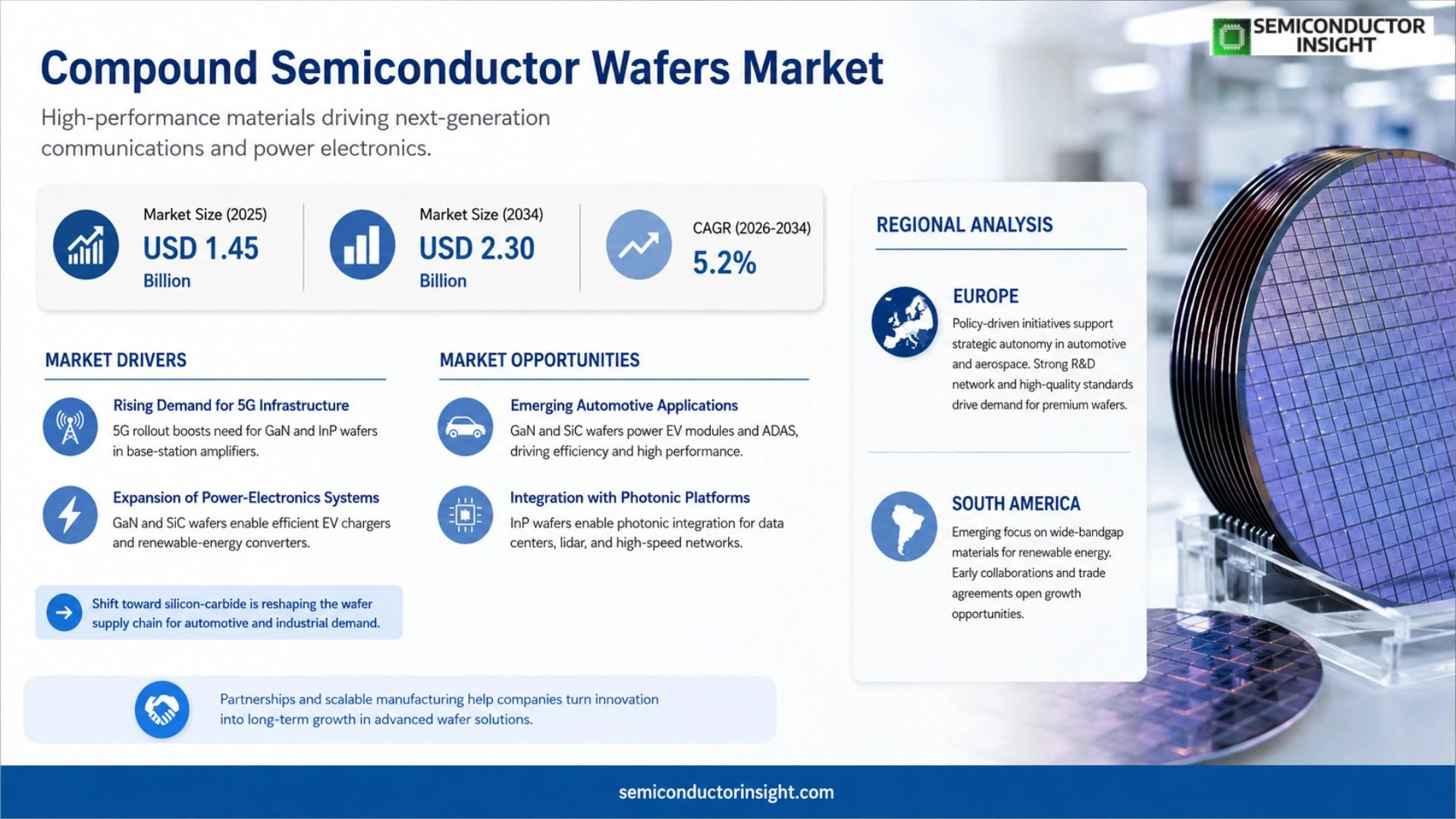
MARKET DRIVERS
Rising Demand for 5G Infrastructure
The rollout of 5G networks accelerates the need for high‑frequency components, and compound semiconductor wafers,especially gallium nitride (GaN) and indium phosphide (InP),deliver the power density and linearity required for base‑station amplifiers. Operators are committing billions to dense urban deployments, compelling wafer suppliers to scale capacity and diversify product lines.
Expansion of Power‑Electronics Systems
Electrification of transport and renewable‑energy converters drives a surge in devices that must operate at higher voltages and temperatures. GaN and silicon‑carbide (SiC) wafers enable lightweight converters for electric‑vehicle chargers and grid‑inverters, prompting OEMs to source larger wafer volumes to meet performance targets while reducing system size.
➤ The shift toward silicon‑carbide is reshaping the wafer supply chain, creating new fulfillment models for high‑volume automotive customers.
Both 5G and power‑electronics trends converge on a common requirement: faster time‑to‑market for advanced devices. This pressure fosters strategic partnerships between fab houses and design firms, aligning capacity planning with product roadmaps and reinforcing the growth trajectory of the Compound Semiconductor Wafers Market.
MARKET CHALLENGES
Manufacturing Complexity and Yield Management
Producing compound semiconductor wafers involves epitaxial growth on substrates that differ from conventional silicon, leading to tighter process windows and higher defect sensitivity. Yield optimization therefore becomes a critical cost factor, as even minor variations can erode profitability for both manufacturers and downstream device makers.
Other Challenges
Supply Chain Volatility
Raw material shortages,particularly high‑purity gallium and indium,have intermittently constrained output. Coupled with geopolitical tensions affecting trade routes, firms must negotiate longer-term contracts and diversify sourcing to mitigate disruptions.
MARKET RESTRAINTS
High Capital Expenditure Requirements
Establishing a mature compound‑semiconductor fab demands multi‑billion‑dollar investments in specialized reactors, metrology tools, and cleanroom infrastructure. Smaller players often lack the financial bandwidth to fund such projects, leading to a market dominated by a few large incumbents and limiting competitive pricing.
Limited Lithography Compatibility
Current photolithography equipment is optimized for silicon wafers; adapting it for wider band‑gap materials incurs additional tooling costs and process development time. This incompatibility slows the transition from prototype to high‑volume production, restraining the overall pace of market expansion.
MARKET OPPORTUNITIES
Emerging Automotive Applications
Electric‑vehicle power modules and advanced driver‑assistance systems (ADAS) increasingly rely on high‑efficiency power amplifiers and sensors built on GaN and SiC substrates. As OEMs pursue higher range and faster charging, Compound Semiconductor Wafers Market participants that can assure consistent quality at scale stand to capture a lucrative vertical.
Integration with Photonic Platforms
Data‑center interconnects and lidar solutions demand integrated photonic circuits, where InP wafers provide superior optical gain. Companies investing in heterogeneous integration,combining silicon photonics with compound wafers,are positioned to create differentiated products that address bandwidth‑intensive workloads.
Strategic focus on collaborative R&D and flexible manufacturing footprints will enable firms to respond swiftly to these emerging niches, translating technical advantage into measurable revenue streams within the Compound Semiconductor Wafers Market.
Compound Semiconductor Wafers Market Trends
Accelerated Adoption of SiC and GaN for High‑Efficiency Power Conversion
The power‑electronics segment is witnessing a clear shift from silicon toward wide‑bandgap materials, principally silicon carbide (SiC) and gallium nitride (GaN). This transition is driven by the need for higher voltage handling, lower conduction losses, and faster switching,attributes that directly support the efficiency targets of electric‑vehicle drivetrains, data‑center power supplies, and renewable‑energy inverters. As manufacturers integrate SiC and GaN wafers into their designs, procurement volumes are expanding beyond niche applications, prompting suppliers to scale capacity and streamline yields. The ripple effect includes tighter price competition, faster product‑introduction cycles, and a reallocation of R&D budgets toward substrate engineering and thermal‑management solutions. For end‑users, the material shift translates into reduced total‑cost‑of‑ownership, which accelerates adoption across both original‑equipment manufacturers (OEMs) and contract manufacturers.
Other Trends
Emergence of Sub‑8‑Inch Wafer Platforms for Cost‑Sensitive Applications
While the majority of high‑performance power devices remain anchored to 8‑inch and larger substrates, a parallel movement is gaining traction among automotive‑grade sensor and analog IC producers. Sub‑8‑inch wafers offer a lower entry barrier for firms targeting volume‑price points below $10 per unit, especially in regions where fab infrastructure favors smaller diameters. This diversification eases capacity constraints on larger fabs, allowing them to focus on premium GaN and SiC runs. Consequently, the supply chain is witnessing a bifurcation: dedicated low‑cost lines for mass‑market analog components and premium high‑throughput lines for wide‑bandgap power devices.
Regional Concentration of Investment in Advanced Packaging and Integration
Asia‑Pacific remains the epicenter of capital deployment, with China and South Korea announcing multi‑billion‑dollar programs to pair SiC/GaN wafers with advanced packaging technologies such as system‑in‑package (SiP) and flip‑chip bonding. Europe’s push toward automotive electrification is prompting Germany and France to subsidize joint‑venture fabs that co‑locate wafer processing and packaging. In North America, the United States is leveraging defense‑related funding to secure a domestic supply of high‑reliability SiC wafers for aerospace applications. These geographically distinct investment patterns are reshaping the competitive landscape, incentivizing incumbent players like Wolfspeed and II‑VI Advanced Materials to form strategic alliances with regional specialists, while newcomers such as TankeBlue focus on niche high‑frequency GaN offerings.
COMPETITIVE LANDSCAPE
Key Industry Players
Compound Semiconductor Wafers – Competitive Overview
Wolfspeed dominates the SiC and GaN wafer segment, leveraging vertically integrated manufacturing and a robust IP portfolio that underpins its ability to service high‑power automotive and industrial customers. Its strategic focus on expanding capacity in the United States and Taiwan has tightened supply chains and forced rivals to reassess their own production footprints. The company’s pricing power stems from a combination of superior material quality and a well‑established customer base that values long‑term reliability, which translates into a decisive advantage in a market where yield differentials can dictate profitability.
Beyond the incumbent, a cluster of specialized firms injects diversity into the competitive set. SK Siltron and II‑VI Advanced Materials have amplified their GaN wafer lines to capture emerging 5G infrastructure demand, while Showa Denko and Norstel concentrate on niche silicon‑carbide applications for power converters. Smaller but technically agile players such as TankeBlue, SICC, Hebei Synlight Crystal, and CETC are carving out regional footholds in Asia, often partnering with local OEMs to tailor wafer thicknesses and doping profiles. This mosaic of scale and specialization creates a landscape where collaboration, joint‑development agreements, and selective acquisitions are common pathways to broaden market reach.
List of Key Compound Semiconductor Wafers Companies Profiled
- Wolfspeed
- SK Siltron
- II-VI Advanced Materials
- Showa Denko
- Norstel
- TankeBlue
- SICC
- Hebei Synlight Crystal
- CETC
- SiCrystal
- Rogers Corporation
- Qorvo
Segment Analysis:
| Segment Category | Sub-Segments | Key Insights |
| By Type |
|
GaN Wafers are emerging as the leading segment due to their high electron mobility and efficiency in power‑dense applications. – They enable compact power converters that meet the stringent thermal management needs of modern data‑center and automotive systems. – The material’s ability to operate at higher frequencies supports advanced RF and 5G infrastructure, driving strong design interest from OEMs. – Industry experts note that GaN’s scalability aligns with evolving IoT device architectures, fostering ecosystem growth. |
| By Application |
|
8‑inch and larger wafers dominate the application landscape because they facilitate higher throughput and lower cost per unit for volume manufacturers. – They are preferred for power‑electronics modules in electric‑vehicle drivetrains where reliability and consistency are paramount. – Larger wafers also support the integration of heterogeneous components, enabling compact RF front‑ends for telecommunications. – Design teams appreciate the flexibility to combine GaN and SiC layers on a single substrate, expanding functional possibilities. |
| By End User |
|
Automotive electronics are a pivotal end‑user segment as manufacturers pursue higher efficiency power‑trains and advanced driver‑assistance systems. – The robustness of SiC wafers aligns with the high‑temperature, high‑stress environment of vehicle power modules. – GaN enables compact on‑board chargers and fast‑charging infrastructure that meet consumer expectations for convenience. – OEMs increasingly view compound semiconductor wafers as strategic enablers for future electrified mobility platforms. |
| By Innovation Trend |
|
Heterogeneous integration is reshaping the market by allowing GaN and SiC devices to be combined with silicon logic on a single platform. – This approach reduces interconnect latency and improves overall system efficiency, a key demand from high‑performance computing and edge‑AI applications. – Researchers emphasize that substrate engineering advances are unlocking new defect‑free crystal growth, enhancing yield and reliability across multiple wafer sizes. |
| By Sustainability Focus |
|
Energy‑efficient manufacturing is gaining traction as manufacturers align with corporate ESG goals. – Process innovations such as low‑temperature epitaxy lower overall power consumption and shrink the carbon footprint of wafer production. – The industry is also exploring recyclable substrate concepts that allow material recovery at end‑of‑life, supporting circular‑economy initiatives. – Stakeholders note that sustainability considerations are increasingly influencing supplier selection and partnership decisions. |
Regional Analysis: Compound Semiconductor Wafers Market
Asia‑Pacific
Universities and corporate labs in the region collaborate on lattice‑matched substrates, delivering wafer recipes that address thermal‑management challenges in power electronics, thereby enhancing device reliability for end‑users.
Multi‑project wafer services have expanded, offering flexible volumes that match the iterative design cycles of chip makers, and reducing time‑to‑market for emerging applications.
Close ties between wafer suppliers and equipment vendors enable coordinated upgrades, ensuring that process tooling evolves in step with material advances.
The region’s push into autonomous transportation and 5G infrastructure creates demand for high‑frequency and high‑power wafers, prompting vendors to tailor offerings to these growth vectors.
North America
North America remains a strong contender in the Compound Semiconductor Wafers Market thanks to its mature ecosystem of design houses and venture capital that fuels early‑stage startups. The emphasis on high‑performance computing and defense electronics drives a focus on gallium arsenide and indium phosphide wafers, where performance margins are critical. Collaboration between academia and industry is reinforced by collaborative research consortia that de‑risk long‑term material development. While the region does not match the sheer volume of production in Asia‑Pacific, its value‑add capabilities and design leadership continue to attract multinational investments seeking differentiated technologies.
Europe
Europe’s approach to the Compound Semiconductor Wafers Market is anchored in policy‑driven initiatives that prioritize strategic autonomy, especially in automotive and aerospace sectors. The region benefits from a dense network of specialized equipment manufacturers, which supports niche wafer processes needed for mixed‑signal and photonic applications. Cross‑border research programs create a shared knowledge base that mitigates fragmentation among national funding bodies. Although the manufacturing footprint is modest compared with Asia‑Pacific, Europe’s emphasis on sustainability and high‑reliability standards positions it as a preferred supplier for premium‑grade wafers.
South America
South America is still defining its role in the Compound Semiconductor Wafers Market, yet nascent clusters are emerging around university research hubs that explore wide‑bandgap materials for renewable‑energy converters. Governments are beginning to recognize the strategic importance of localizing wafer production to reduce dependence on imported components. Early‑stage collaborations with Asian partners provide technology transfer pathways, while regional trade agreements open channels for export of specialized wafer services to neighboring markets.
Middle East & Africa
The Middle East & Africa region is gradually entering the conversation on compound semiconductor wafers, driven primarily by sovereign wealth funds allocating capital to high‑tech ventures. Pilot projects focused on satellite communications and defense illustrate a willingness to invest in advanced wafer technologies. Partnerships with established global fabs are being forged to bypass the steep capital requirements of building full‑scale production. While the market share remains limited, the strategic intent signals a longer‑term ambition to develop a self‑sustaining supply chain for critical applications.
Report Scope
This market research report provides a comprehensive analysis of the Compound Semiconductor Wafers Market , covering the forecast period 2026–2034. It offers detailed insights into market dynamics, technological advancements, competitive landscape, and key trends shaping the industry.
Key focus areas of the report include:
- Market Overview: The report begins with an overview outlining its current market scenario, key growth indicators, and industry transformation drivers. It discusses macroeconomic factors, demand–supply balance, regulatory landscape, and the strategic role of semiconductors in powering advancements across industries such as automotive, telecommunications, consumer electronics, and industrial automation.
- Market Size & Forecast: Historical data and future projections for revenue, unit shipments, and market value across major regions and segments.
- Segmentation Analysis: Detailed breakdown by product type, technology, application, and end-user industry to identify high-growth segments and investment opportunities.
- Regional Insights: Insights into market performance across North America, Europe, Asia-Pacific, Latin America, and the Middle East & Africa, including country-level analysis where relevant.
- Competitive Landscape: Profiles of leading market participants, including their product offerings, R&D focus, manufacturing capacity, pricing strategies, and recent developments such as mergers, acquisitions, and partnerships.
- Technology Trends & Innovation: Assessment of emerging technologies, integration of AI/IoT, semiconductor design trends, fabrication techniques, and evolving industry standards.
- Market Drivers & Restraints: Evaluation of factors driving market growth along with challenges, supply chain constraints, regulatory issues, and market-entry barriers.
- Stakeholder Insights: Insights for component suppliers, OEMs, system integrators, investors, and policymakers regarding the evolving ecosystem and strategic opportunities.
Primary and secondary research methods are employed, including interviews with industry experts, data from verified sources, and real-time market intelligence to ensure the accuracy and reliability of the insights presented.
FREQUENTLY ASKED QUESTIONS:
What is the current market size of Compound Semiconductor Wafers Market?
-> Compound Semiconductor Wafers market is projected to grow from USD 1.55 billion in 2026 to USD 2.30 billion by 2034, exhibiting a CAGR of 5.2%
Which key companies operate in Compound Semiconductor Wafers Market?
-> Key players include Wolfspeed, SK Siltron, SiCrystal, II-VI Advanced Materials, Showa Denko, Norstel, TankeBlue, SICC, Hebei Synlight Crystal, CETC, among others.
What are the key growth drivers?
-> Key growth drivers include rising demand for high‑efficiency power devices, expansion of automotive electrification, and increasing adoption of IoT and 5G technologies.
Which region dominates the market?
-> Asia remains the largest and fastest‑growing region, driven by strong manufacturing capacity and adoption of SiC and GaN technologies.
What are the emerging trends?
-> Emerging trends include greater integration of SiC and GaN in power‑electronics, miniaturization of wafer formats, and the development of advanced packaging solutions.

Get Sample Report PDF for Exclusive Insights
Report Sample Includes
- Table of Contents
- List of Tables & Figures
- Charts, Research Methodology, and more...
 Download Sample Report PDF



