Key Statistics
Key Takeaways
- HBM3E is the leading source-page type segment because the page explicitly describes it as the preferred current generation for cutting-edge AI accelerators and high-performance GPUs. HBM4 is transitioning from development into commercial production in 2026, while HBM3 remains relevant for established systems and cost-sensitive deployments.
- Artificial Intelligence & Machine Learning Accelerators dominate the source-page application landscape because training and inference systems require extremely high memory bandwidth and capacity per compute package. Hyperscale Cloud Service Providers are separately identified as the dominant end-user segment, anchoring recurring procurement through large AI-cluster buildouts.
- Asia Pacific leads the market because South Korea hosts the three-way HBM supply contest among SK hynix and Samsung alongside Micron’s global competition, Taiwan provides critical advanced-packaging infrastructure, and Japan supplies key materials and equipment. North America remains the most influential demand-side design region.
- HBM4 commercialization accelerated materially in 2026. Samsung announced commercial HBM4 shipment in February, Micron began high-volume HBM4 shipments in the first calendar quarter, and SK hynix said HBM4 mass shipments began while also sampling HBM4E to major customers.
- The source-page 2025 and 2034 endpoints do not reconcile with its printed 2026 value or CAGR. USD 4.21 billion in 2025 and USD 51.24 billion in 2034 imply approximately 32.0% CAGR and a mathematically consistent 2026 value of about USD 5.56 billion, rather than the printed USD 5.38 billion and 28.4% CAGR.
High Bandwidth Memory (HBM3, HBM3E, HBM4) Market Overview
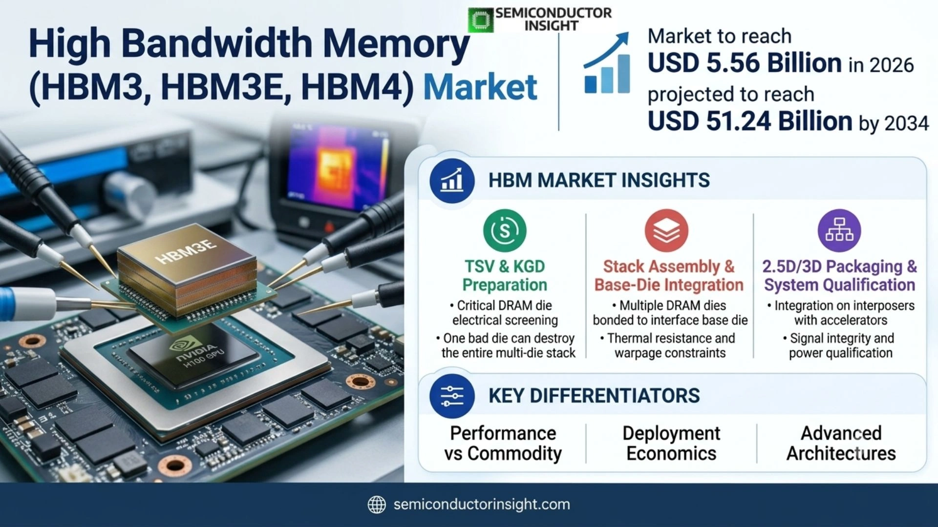
High Bandwidth Memory (HBM3, HBM3E, HBM4) market is valued at USD 4.21 billion in 2025, increases to an estimated USD 5.56 billion in 2026, and is projected to reach USD 51.24 billion by 2034. The selected source-page size anchors imply a 32.0% CAGR during 2026–2034. Asia Pacific is the largest market in 2025 because the source-page regional analysis explicitly calls Asia-Pacific the dominant force and its FAQ also identifies the region as a leading HBM market, while current demand is being reshaped by AI accelerator deployment, HBM4 and HBM4E qualification, 2.5D and hybrid-bonding packaging, higher memory bandwidth per accelerator, sovereign AI infrastructure, advanced packaging expansion and long-term supply agreements between memory vendors and compute-platform customers.
High Bandwidth Memory is a vertically stacked DRAM architecture that connects multiple memory dies through through-silicon vias and very wide interfaces to deliver far more bandwidth per package than conventional DDR or GDDR. HBM3, HBM3E and HBM4 progressively increase bandwidth, capacity and power efficiency while reducing the energy spent moving data between processor and memory. The architecture is therefore central to modern GPUs, AI accelerators and scientific-computing systems where arithmetic throughput would otherwise be underutilized because memory cannot feed data fast enough.
The 2026 commercialization cycle is substantially more advanced than the older source-page narrative implies. Samsung announced mass production and commercial shipment of HBM4 in February 2026, Micron began volume shipment of 36GB 12-high HBM4 in the first quarter, and SK hynix stated in July that HBM4 mass shipments had begun. All three suppliers are already discussing or sampling HBM4E, indicating that the market is transitioning generations faster than the original HBM3E-centered source text suggests while still preserving HBM3E as the leading current source-page segment.
Demand is structurally linked to accelerator architecture and package availability. HBM cannot be deployed independently of logic-die integration, silicon interposers, advanced substrates, thermal design and package yield. That makes TSMC, ASE, Amkor and other packaging participants strategically important even though SK hynix, Samsung and Micron control the DRAM supply. Hyperscale cloud providers and AI chip designers increasingly negotiate supply and co-development arrangements several years ahead because HBM availability can constrain the number of complete AI accelerators that reach the market.
Segment Analysis: By Type
The source page segments the market into HBM3, HBM3E and HBM4. HBM3E is explicitly identified as the leading current segment because of rapid adoption in AI accelerators, while HBM4 is positioned as the next dominant generation as bandwidth, interface width and capacity requirements rise. The 2026 market now includes commercial HBM4 shipments, so current external evidence is used to update commercialization status without changing the source segmentation.
| Type | Technical / commercial role | Market position |
|---|---|---|
| HBM3 | HBM3 widened the memory interface and raised per-stack bandwidth for accelerators, HPC systems and GPUs compared with HBM2E. It remains deployed in existing systems and provides a cost/performance bridge where the newest HBM3E or HBM4 generation is not essential. Product economics depend on stack height, known-good-die yield, TSV integrity and advanced package compatibility. | Transitional but durable source-page segment. Installed AI and HPC platforms keep HBM3 demand active, but new flagship accelerator roadmaps are moving toward HBM3E and HBM4. Suppliers therefore manage HBM3 capacity alongside faster-generation ramps rather than treating it as the long-term premium growth engine. |
| HBM3E | HBM3E extends HBM3 with higher pin speed, capacity and power efficiency and is widely used in current AI accelerators. It requires mature TSV stacking, thermal management and package co-design because higher throughput increases heat flux and signal-integrity sensitivity. The generation became the commercial workhorse for large AI-training systems before HBM4 volume availability broadened. | Leading source-page type. The page explicitly identifies HBM3E as the current market leader. Even with HBM4 ramping in 2026, HBM3E remains important for existing accelerator platforms and large installed procurement programs whose qualification cycles predate HBM4. |
| HBM4 | HBM4 doubles the interface width to 2,048 bits and raises per-stack bandwidth beyond HBM3E while allowing larger capacity and deeper compute-memory co-design. Commercial 2026 products from Samsung and Micron exceed 11 Gb/s per pin, and HBM4 roadmaps increasingly use advanced logic base dies and next-generation bonding to manage bandwidth, power and thermal density. | Fastest strategic transition. Samsung announced commercial shipment in February 2026, Micron entered high-volume production in the first calendar quarter, and SK hynix reported mass shipments beginning by July. HBM4 is therefore no longer merely an anticipated source-page technology but an active production market. |
Secondary segmentation: By End User
The source page identifies Hyperscale Cloud Service Providers, AI Hardware Manufacturers & Semiconductor Companies, Research & Academic Institutions / HPC Centers and Telecommunications & Networking Companies. Hyperscale cloud providers are explicitly described as the dominant end-user segment because they finance large accelerator clusters and recurring capacity additions. For HBM suppliers, the commercial consequence is that DRAM yield, stack height, thermal resistance, base-die integration and advanced-package availability determine revenue quality much more directly than headline AI accelerator shipments.
| End user | Commercial characteristics |
|---|---|
| Hyperscale Cloud Service Providers | Cloud and AI infrastructure operators buy accelerators at enormous scale and increasingly secure long-term memory supply indirectly through GPU and custom-silicon roadmaps. Their purchasing decisions determine which HBM generation ramps fastest and whether capacity is reserved several years ahead. |
| AI Hardware Manufacturers & Semiconductor Companies | GPU, accelerator and custom-ASIC designers co-design memory interfaces, package geometry, power delivery and thermal systems with HBM suppliers. NVIDIA and AMD are named on the source page as major demand drivers, while memory suppliers increasingly align HBM4/HBM4E roadmaps directly with accelerator platforms. |
| Research & Academic Institutions / HPC Centers | National laboratories and supercomputing centers use HBM-equipped accelerators for scientific simulation, climate, genomics and AI research. Procurement volumes are smaller than hyperscalers but system lifecycles are long and performance requirements can help validate new memory generations. |
| Telecommunications & Networking Companies | High-radix switches, packet-processing ASICs and AI-enabled network systems can use HBM where packet tables, buffering or real-time analytics require exceptional bandwidth. The source page lists networking as an expanding application beyond the core AI accelerator market. |
Secondary segmentation: By Technology Architecture
The source page divides HBM integration into 2.5D Integration (Interposer-Based), 3D Stacking with Through-Silicon Via (TSV), and Hybrid Bonding & Advanced Packaging. It identifies 2.5D silicon-interposer integration as the current leading deployment architecture while hybrid bonding gains importance for HBM4 and future generations. This distinction matters because HBM3, HBM3E and HBM4 require different interface, power and package designs, so capacity cannot be shifted instantly between generations after a customer platform is qualified.
| Technology architecture | Market implication |
|---|---|
| 2.5D Integration (Interposer-Based) | Silicon interposers place logic and HBM stacks side by side with very wide, short electrical paths. The architecture is proven in leading GPUs and AI accelerators and supports dense routing that conventional organic substrates cannot easily provide. Package size, interposer yield and advanced packaging capacity are major cost drivers. |
| 3D Stacking with Through-Silicon Via (TSV) | TSVs vertically connect multiple DRAM dies inside each HBM stack and are foundational to every HBM generation. Yield depends on die thinning, via quality, thermal stress and stacking precision, making the memory package far more complex than conventional planar DRAM. |
| Hybrid Bonding & Advanced Packaging | Hybrid copper bonding and other fine-pitch interconnect technologies can reduce thermal and electrical resistance while enabling more layers and denser logic-memory integration. Samsung’s 2026 HBM roadmap explicitly highlights hybrid copper bonding for 16-layer-plus future HBM, showing how packaging becomes a product-generation enabler. |
Secondary segmentation: By Supply Chain Tier
The source page separates HBM DRAM Manufacturers, Advanced Packaging & Assembly Providers, and System Integrators & OEM Partners. Tier 1 memory producers have the greatest direct control over HBM availability, but advanced packaging is a co-equal practical bottleneck because a memory stack has no market value until it is integrated successfully with compute silicon.
| Supply-chain tier | Commercial role |
|---|---|
| HBM DRAM Manufacturers (Tier 1) | SK hynix, Samsung and Micron design and manufacture the DRAM dies, stack them and qualify each HBM generation. Their fab, TSV, bonding and yield roadmaps determine the volume of saleable HBM and the timing of HBM3E, HBM4 and HBM4E transitions. |
| Advanced Packaging & Assembly Providers (Tier 2) | TSMC, ASE, Amkor and related substrate/package suppliers integrate HBM stacks with accelerator dies using interposers, advanced substrates and thermal structures. Capacity constraints at this stage can cap accelerator output even if raw HBM stack availability improves. |
| System Integrators & OEM Partners (Tier 3) | NVIDIA, AMD, server OEMs and cloud operators specify final platform requirements and validate thermal, signal and reliability behavior. Their architecture choices create the demand signal that memory suppliers use when allocating multiyear capacity. |
Segment Analysis: By Application
By application, the source page segments demand into Artificial Intelligence & Machine Learning Accelerators, High-Performance Computing (HPC), Graphics Processing Units (GPUs), Network Switching & Routing, and Others. AI & Machine Learning Accelerators are explicitly identified as the dominant application because model training and inference create the most severe bandwidth and capacity requirements.
| Application | Demand characteristics |
|---|---|
| Artificial Intelligence & Machine Learning Accelerators | Frontier training and inference accelerators pair very high compute throughput with multiple HBM stacks to keep matrix engines fed with data. The size of models, context windows and batch processing increases both bandwidth and capacity demand, making memory architecture a direct limiter of accelerator utilization. HBM4 products are already designed around next-generation AI platforms. |
| High-Performance Computing (HPC) | Scientific simulation, climate modeling, genomics and national supercomputing use HBM to sustain memory-intensive workloads across GPU or accelerator clusters. The segment values deterministic sustained bandwidth and system reliability and can adopt new HBM generations where time-to-solution justifies premium cost. |
| Graphics Processing Units (GPUs) | Professional graphics, visualization and GPU compute use HBM where wide memory interfaces improve throughput. The application increasingly overlaps with AI because modern GPUs serve both graphics and tensor workloads, so HBM demand is often driven by the same compute platforms across different end uses. |
| Network Switching & Routing | High-capacity networking ASICs can use HBM for large tables, buffering and real-time packet analytics. AI fabrics also increase switch bandwidth and may create memory-intensive processing functions at the network edge, broadening HBM’s role beyond accelerator packages. |
| Others | Other uses include defense computing, automotive AI and specialized edge systems. These applications remain smaller because HBM cost and packaging complexity are difficult to justify unless bandwidth is a first-order system bottleneck. |
Regional Analysis
The source page explicitly says Asia-Pacific firmly anchors itself as the dominant force in HBM, with South Korea as the innovation core, Taiwan as the advanced-packaging powerhouse, Japan as a materials/equipment supplier and China as an emerging localization market. North America is described separately as the most influential demand-side region.
Why are HBM production leadership and demand-side architecture leadership concentrated in different regions?
HBM requires both advanced DRAM fabrication and complex packaging. South Korea hosts major memory suppliers, Taiwan hosts leading logic and advanced packaging, and Japan supplies critical materials and equipment, giving Asia Pacific the strongest production ecosystem. North America contains NVIDIA, AMD and hyperscale cloud companies that define accelerator roadmaps and therefore strongly influence memory specifications. Europe, South America and MEA are primarily end-demand and research markets whose HBM consumption arrives through imported accelerator systems.
| Region | Position | Growth outlook | Demand profile | What decides supplier selection |
|---|---|---|---|---|
| Asia Pacific | Largest production market | Very high | HBM manufacturing, advanced packaging and AI infrastructure-led | Yield, stack technology, packaging capacity and customer qualification |
| North America | Most influential demand-side region | Very high | AI accelerator, cloud and custom silicon-led | Platform co-design, supply agreements and performance per watt |
| Europe | Strategic HPC and sovereign-AI market | High | HPC, research and advanced integration-led | System qualification, imported accelerator availability and packaging research |
| South America | Emerging end market | Moderate from small base | Cloud and enterprise AI adoption-led | Access to accelerator systems, data-center scale and import economics |
| Middle East & Africa | Rapid sovereign-AI demand market | High from small base | Gulf AI factories and sovereign compute-led | Accelerator availability, power infrastructure and long-term supply |
Competitive Landscape
The source page profiles fifteen ecosystem participants: SK Hynix, Samsung Electronics, Micron Technology, NVIDIA, AMD, TSMC, ASE Technology, Rambus, Cadence, Synopsys, Intel, Amkor Technology, JEDEC, Graphcore and Cerebras Systems. The list intentionally extends beyond HBM DRAM manufacturers to packaging, accelerator, IP and standards participants; JEDEC is an industry standards association rather than a commercial company, and that source-page distinction is preserved.
SK hynix, Samsung and Micron form the core HBM memory-manufacturing tier and control the direct supply of HBM stacks. Competition is increasingly based on HBM4/HBM4E speed, power efficiency, stack height, thermal resistance, logic-base-die design and yield. Supplier qualification with NVIDIA, AMD and hyperscale customers is strategically important because a leading specification has limited commercial value until it is accepted on a high-volume accelerator platform.
NVIDIA, AMD, Intel, Graphcore and Cerebras are demand-side compute companies whose memory architectures define bandwidth and capacity requirements. NVIDIA and AMD have particularly strong influence because their accelerator roadmaps absorb large HBM volumes and can trigger multiyear supplier allocations. Intel’s role varies by accelerator roadmap, while Graphcore and Cerebras represent alternative AI architectures and are preserved because the source page includes them.
TSMC, ASE and Amkor supply advanced packaging and assembly capabilities, while Rambus, Cadence and Synopsys contribute interface IP, PHY/verification and design-tool support. JEDEC defines industry standards and is therefore not a supplier in the same commercial sense. This broader ecosystem view is appropriate because HBM performance and shipment volume depend on memory, packaging, logic and standards evolving together.
| Competitive tier | Companies | Why they matter |
|---|---|---|
| HBM memory manufacturers | SK Hynix Inc.; Samsung Electronics Co., Ltd.; Micron Technology, Inc. | These three suppliers control commercially available leading HBM production and determine stack supply, generation timing, manufacturing yield and direct customer qualification. |
| Compute and system demand drivers | NVIDIA Corporation; Advanced Micro Devices, Inc. (AMD); Intel Corporation; Graphcore Limited; Cerebras Systems | These companies integrate or influence high-bandwidth-memory architectures in AI and HPC compute. Their platform roadmaps determine HBM speed, capacity, interface and packaging requirements. |
| Packaging, IP, EDA and standards ecosystem | TSMC; ASE Technology; Amkor Technology; Rambus; Cadence Design Systems; Synopsys; JEDEC Solid State Technology Association | These participants enable physical integration, interface design, verification and standardization. JEDEC is a standards association rather than a commercial semiconductor vendor but is retained because it appears in the source profile list. |
Companies profiled in the report
The source page profiles SK Hynix Inc.; Samsung Electronics Co., Ltd.; Micron Technology, Inc.; NVIDIA Corporation; Advanced Micro Devices, Inc. (AMD); Taiwan Semiconductor Manufacturing Company (TSMC); ASE Technology Holding Co., Ltd.; Rambus Inc.; Cadence Design Systems, Inc.; Synopsys, Inc.; Intel Corporation; Amkor Technology, Inc.; JEDEC Solid State Technology Association; Graphcore Limited; and Cerebras Systems.
Production Capacity Analysis
HBM production capacity is constrained by DRAM wafer output, known-good-die yield, TSV formation, wafer thinning, stacking, molding or bonding, logic-base-die supply and final advanced-package capacity. Increasing wafer starts alone does not create saleable HBM if stacking or package yield is insufficient. The 2026 cycle shows all three major memory suppliers ramping HBM4 while advanced packaging remains a strategic co-bottleneck.
SK hynix reported HBM4 mass shipment in 2026 and long-term agreements with around ten key customers, demonstrating capacity being allocated against multiyear demand visibility. The company is also sampling HBM4E and using advanced MR-MUF packaging to reduce thermal resistance. This means effective output depends on both DRAM fab capacity and proprietary stacking/packaging process capability.
Samsung began mass production and commercial shipment of HBM4 in February 2026 using 1c DRAM and a 4 nm logic base die, then shipped HBM4E samples in May. The company’s roadmap also includes hybrid copper bonding for higher stack counts, showing that base-die and bonding capacity must scale together as HBM generations become more integrated.
Micron entered high-volume HBM4 production in the first quarter of 2026 and sampled 48GB 16-high products. Its current HBM4 specification provides more than 2.8 TB/s per stack. Production economics therefore depend on maintaining high yields across many thin DRAM dies and integrating them reliably with a wide 2,048-bit interface and downstream accelerator package.
Market Dynamics
The market is driven by AI compute, higher model size, HPC and sovereign infrastructure, but it is restrained by concentrated supply, advanced packaging bottlenecks, thermal density, cost and generation-ramp yield. HBM is strategically valuable because it can increase accelerator utilization, yet its unusually complex manufacturing flow makes supply much less elastic than conventional commodity DRAM.
Market Drivers
| Driver | Directional impact* | Commercial mechanism |
|---|---|---|
| AI accelerator scaling | High | More compute units and larger models require greater bandwidth and capacity per accelerator package, making HBM a core architectural component. |
| HBM4 generation transition | High | A wider interface and higher per-pin speed materially increase bandwidth, creating replacement and premium-product demand. |
| Hyperscale & sovereign AI investment | High | Large AI factories and cloud clusters buy accelerators in multiyear programs, sustaining HBM demand and encouraging supplier capacity commitments. |
| Advanced packaging expansion | High | More interposer, hybrid-bonding and substrate capacity allows a larger number of HBM-equipped accelerators to reach market. |
AI compute throughput is increasingly memory constrained
Adding tensor and matrix units to an accelerator creates limited value if model weights and activations cannot be delivered quickly enough. HBM provides extremely wide interfaces and high bandwidth per watt, allowing processor arithmetic units to remain better utilized. This makes memory a performance feature of the accelerator rather than a secondary commodity component.
Model capacity raises both bandwidth and memory-capacity requirements
Large language and multimodal models need enormous parameter and KV-cache capacity while sustaining rapid token throughput. HBM4 and HBM4E increase stack capacity and bandwidth, allowing more model state to remain close to compute. As context windows grow, the commercial value of additional memory capacity per accelerator also rises. For HBM suppliers, the commercial consequence is that DRAM yield, stack height, thermal resistance, base-die integration and advanced-package availability determine revenue quality much more directly than headline AI accelerator shipments.
Sovereign AI creates new large procurement programs
Saudi Arabia and other governments are funding AI factories with tens of thousands of accelerators. These programs add demand outside the traditional U.S. hyperscaler base and create multi-year visibility for HBM suppliers, provided memory and package capacity can be synchronized with accelerator delivery. This distinction matters because HBM3, HBM3E and HBM4 require different interface, power and package designs, so capacity cannot be shifted instantly between generations after a customer platform is qualified.
Advanced packaging unlocks saleable HBM systems
A complete AI processor depends on HBM stacks, logic dies, interposers, substrates and thermal management. Expanding CoWoS-equivalent and hybrid-bonding capacity therefore increases the number of HBM-enabled systems that can ship, turning packaging investment into a direct market-growth enabler. Buyers therefore evaluate bandwidth, capacity, power efficiency, package thermals, multiyear supply assurance and accelerator qualification rather than treating HBM as interchangeable commodity DRAM.
Market Restraints
| Restraint | Directional impact* | Commercial mechanism |
|---|---|---|
| Supply concentration | High | Three memory suppliers control leading commercial HBM, limiting short-term substitution when yield or qualification issues occur. |
| Advanced packaging bottlenecks | High | Interposer, substrate and assembly capacity can constrain accelerator output independently of HBM die availability. |
| Thermal density | High | More layers, wider interfaces and higher bandwidth create heat-removal challenges inside dense accelerator packages. |
| Manufacturing cost & yield | High | TSV stacking, die thinning, base-die integration and tight known-good-die requirements make HBM structurally more expensive than conventional DRAM. |
The supplier base is exceptionally concentrated
SK hynix, Samsung and Micron represent the primary commercial HBM memory suppliers. Customers cannot switch instantly because each generation must be qualified for speed, thermals and package behavior. This gives suppliers pricing power but also creates systemic risk if one vendor experiences a yield or production problem. Through 2034, suppliers that synchronize wafer fabrication with TSV stacking and advanced packaging can capture more value as HBM4E and higher-layer architectures increase memory content per accelerator.
Advanced packaging can become the actual shipment bottleneck
HBM stacks are valuable only when integrated with compute silicon. Silicon interposers, substrates, bonding, assembly and final package yield can therefore cap accelerator shipments even if DRAM wafer supply rises. Memory and packaging capacity must be planned as one coordinated system. The market implication is that announced wafer or stack capacity becomes saleable only after known-good-die yield, package integration and customer-platform validation are stable enough for high-volume AI deployments.
Thermal management becomes harder with every generation
Higher bandwidth and taller stacks concentrate more power close to hot accelerator logic. Suppliers are reducing thermal resistance through packaging innovations, but data-center operators also need better cooling. A design that meets electrical performance but cannot sustain temperature under AI workloads will not achieve broad deployment. For HBM suppliers, the commercial consequence is that DRAM yield, stack height, thermal resistance, base-die integration and advanced-package availability determine revenue quality much more directly than headline AI accelerator shipments.
HBM economics remain premium
Stacking many known-good DRAM dies, using TSVs and integrating wide interfaces creates a structural cost premium relative to conventional memory. HBM therefore remains concentrated in workloads where bandwidth has high economic value, limiting rapid adoption in cost-sensitive edge or mainstream consumer devices. This distinction matters because HBM3, HBM3E and HBM4 require different interface, power and package designs, so capacity cannot be shifted instantly between generations after a customer platform is qualified.
Market Opportunities
HBM4E and customized base dies
Samsung and SK hynix are already sampling HBM4E, while Micron has discussed HBM4E customization. Logic base dies can become more tightly co-designed with accelerator platforms, creating higher-value differentiated memory products rather than one standardized commodity stack. Buyers therefore evaluate bandwidth, capacity, power efficiency, package thermals, multiyear supply assurance and accelerator qualification rather than treating HBM as interchangeable commodity DRAM.
Hybrid bonding and 16-layer stacks
Hybrid copper bonding can reduce interconnect and thermal resistance and support higher layer counts. This creates an opportunity to raise capacity per HBM placement without increasing package footprint proportionally. Through 2034, suppliers that synchronize wafer fabrication with TSV stacking and advanced packaging can capture more value as HBM4E and higher-layer architectures increase memory content per accelerator.
Networking and edge AI
The source page identifies network switching, routing and automotive/edge AI as expansion opportunities. If bandwidth requirements exceed conventional DRAM capability, HBM can broaden beyond GPU-centric deployments into specialized high-performance ASICs. The market implication is that announced wafer or stack capacity becomes saleable only after known-good-die yield, package integration and customer-platform validation are stable enough for high-volume AI deployments.
Regional packaging resilience
New advanced-package capacity in the United States, Japan, Korea and Europe can diversify integration risk. Memory suppliers and accelerator designers can use multiple package sites once processes are qualified, reducing dependence on a single geographic bottleneck. For HBM suppliers, the commercial consequence is that DRAM yield, stack height, thermal resistance, base-die integration and advanced-package availability determine revenue quality much more directly than headline AI accelerator shipments.
Supply Chain Analysis
Advanced DRAM wafer fabrication
TSV, thinning & known-good-die preparation
Stack assembly & base-die integration
2.5D/3D accelerator packaging & system qualification
Advanced DRAM wafer fabrication
HBM DRAM dies are fabricated on advanced DRAM nodes with strict yield and power requirements. Wafer capacity and process maturity determine the pool of candidate dies available for stacking. This distinction matters because HBM3, HBM3E and HBM4 require different interface, power and package designs, so capacity cannot be shifted instantly between generations after a customer platform is qualified.
TSV, thinning & known-good-die preparation
DRAM dies are thinned and connected using through-silicon vias. Electrical screening is critical because one bad die can destroy the value of an entire multi-die stack. Buyers therefore evaluate bandwidth, capacity, power efficiency, package thermals, multiyear supply assurance and accelerator qualification rather than treating HBM as interchangeable commodity DRAM. This makes deployment economics directly dependent on application-specific qualification and sustained production support.
Stack assembly & base-die integration
Multiple DRAM dies are bonded or molded into an HBM stack and connected to a logic or interface base die. Thermal resistance, warpage and interconnect yield are key production constraints. Through 2034, suppliers that synchronize wafer fabrication with TSV stacking and advanced packaging can capture more value as HBM4E and higher-layer architectures increase memory content per accelerator.
2.5D/3D accelerator packaging & system qualification
HBM stacks are integrated beside accelerator logic on interposers and advanced substrates, then qualified for signal integrity, power, thermals and reliability. This final stage determines whether the memory can ship inside high-volume AI systems. The market implication is that announced wafer or stack capacity becomes saleable only after known-good-die yield, package integration and customer-platform validation are stable enough for high-volume AI deployments.
Recent Developments
Recent primary-source developments show HBM4 moving into volume production while HBM4E and new three-dimensional memory concepts are already entering the roadmap. The developments below are official supplier announcements and are listed newest first. For HBM suppliers, the commercial consequence is that DRAM yield, stack height, thermal resistance, base-die integration and advanced-package availability determine revenue quality much more directly than headline AI accelerator shipments.
August 4, 2026 – Samsung unveiled zHBM and its next-generation AI-memory roadmap
Samsung introduced a zHBM concept that vertically stacks HBM above AI accelerators and said a next-generation interface could deliver about eight times HBM5 performance while increasing density and improving thermal behavior. The announcement shows the industry already exploring architectures beyond conventional side-by-side HBM packages. This distinction matters because HBM3, HBM3E and HBM4 require different interface, power and package designs, so capacity cannot be shifted instantly between generations after a customer platform is qualified.
July 29, 2026 – SK hynix reported HBM4 mass shipments and multiyear customer agreements
SK hynix said HBM4 mass shipments had begun and highlighted long-term agreements with around ten key customers amid record AI-memory demand. The update provides direct evidence that HBM4 has moved beyond sampling into commercial shipment and that capacity is increasingly secured through multiyear agreements. Buyers therefore evaluate bandwidth, capacity, power efficiency, package thermals, multiyear supply assurance and accelerator qualification rather than treating HBM as interchangeable commodity DRAM.
June 18, 2026 – SK hynix shipped 12-layer HBM4E samples to major customers
SK hynix announced shipment of HBM4E samples with maximum speed of 16 Gb/s per pin, more than 20% higher power efficiency and Advanced MR-MUF packaging that reduces thermal resistance. The product extends the supplier race immediately beyond the first HBM4 generation. Through 2034, suppliers that synchronize wafer fabrication with TSV stacking and advanced packaging can capture more value as HBM4E and higher-layer architectures increase memory content per accelerator.
May 29, 2026 – Samsung began shipping HBM4E samples
Samsung announced shipment of 12-layer HBM4E samples to major global customers with speed up to 16 Gb/s per pin and improved thermal and energy performance. The announcement followed commercial HBM4 production only months earlier, illustrating the rapid cadence of the AI-memory roadmap. The market implication is that announced wafer or stack capacity becomes saleable only after known-good-die yield, package integration and customer-platform validation are stable enough for high-volume AI deployments.
March 18, 2026 – Samsung and AMD expanded collaboration on HBM4
Samsung and AMD announced an MOU covering HBM4 supply for AMD Instinct MI455X GPUs and broader next-generation AI memory and computing collaboration. The agreement directly links HBM4 production with a high-volume accelerator roadmap and reinforces customer-specific co-development. For HBM suppliers, the commercial consequence is that DRAM yield, stack height, thermal resistance, base-die integration and advanced-package availability determine revenue quality much more directly than headline AI accelerator shipments.
March 16, 2026 – Micron entered high-volume production of HBM4 for NVIDIA Vera Rubin
Micron announced that 36GB 12-high HBM4 was in high-volume production and volume shipment for NVIDIA Vera Rubin, delivering more than 2.8 TB/s bandwidth and over 20% better power efficiency than its HBM3E comparison. Micron also sampled 48GB 16-high HBM4 products. This distinction matters because HBM3, HBM3E and HBM4 require different interface, power and package designs, so capacity cannot be shifted instantly between generations after a customer platform is qualified.
February 12, 2026 – Samsung began commercial HBM4 shipment
Samsung announced mass production and commercial shipment of HBM4 using sixth-generation 10 nm-class DRAM and a 4 nm logic base die. The product delivered 11.7 Gb/s consistent speed with headroom to 13 Gb/s, marking one of the first major commercial transitions from HBM3E to HBM4. Buyers therefore evaluate bandwidth, capacity, power efficiency, package thermals, multiyear supply assurance and accelerator qualification rather than treating HBM as interchangeable commodity DRAM.
Report Scope & Segmentation
| Attribute | Coverage |
|---|---|
| Market | High Bandwidth Memory (HBM3, HBM3E, HBM4) |
| Base Year | 2025 |
| Estimated Year | 2026 |
| Forecast Period | 2026–2034 |
| 2025 Market Size | USD 4.21 billion |
| 2034 Forecast Size | USD 51.24 billion |
| CAGR | 32.0% (2026–2034) |
| Largest Market in 2025 | Asia Pacific |
| By Type | HBM3; HBM3E; HBM4 |
| By Application | Artificial Intelligence & Machine Learning Accelerators; High-Performance Computing (HPC); Graphics Processing Units (GPUs); Network Switching & Routing; Others |
| By End User | Hyperscale Cloud Service Providers; AI Hardware Manufacturers & Semiconductor Companies; Research & Academic Institutions / HPC Centers; Telecommunications & Networking Companies |
| By Technology Architecture | 2.5D Integration (Interposer-Based); 3D Stacking with Through-Silicon Via (TSV); Hybrid Bonding & Advanced Packaging |
| By Supply Chain Tier | HBM DRAM Manufacturers (Tier 1 Suppliers); Advanced Packaging & Assembly Providers (Tier 2); System Integrators & OEM Partners (Tier 3) |
| Regions | Asia Pacific; North America; Europe; South America; Middle East & Africa |
| Companies Profiled | SK Hynix Inc.; Samsung Electronics Co., Ltd.; Micron Technology, Inc.; NVIDIA Corporation; Advanced Micro Devices, Inc. (AMD); Taiwan Semiconductor Manufacturing Company (TSMC); ASE Technology Holding Co., Ltd.; Rambus Inc.; Cadence Design Systems, Inc.; Synopsys, Inc.; Intel Corporation; Amkor Technology, Inc.; JEDEC Solid State Technology Association; Graphcore Limited; Cerebras Systems |
Frequently Asked Questions
What is the High Bandwidth Memory market size in 2025?
The source page publishes a 2025 market size of USD 4.21 billion. Using the same source page’s USD 51.24 billion 2034 endpoint implies a mathematically consistent 2026 estimate of approximately USD 5.56 billion and an annual compound growth rate of about 32.0%. Through 2034, suppliers that synchronize wafer fabrication with TSV stacking and advanced packaging can capture more value as HBM4E and higher-layer architectures increase memory content per accelerator.
What is the projected HBM market size by 2034?
The source-page 2034 endpoint is USD 51.24 billion. Because both 2025 and 2034 values are published directly, those two size anchors control the article’s forecast arithmetic rather than an external market estimate. The market implication is that announced wafer or stack capacity becomes saleable only after known-good-die yield, package integration and customer-platform validation are stable enough for high-volume AI deployments.
Why is the CAGR 32.0% instead of the page’s 28.4%?
USD 4.21 billion in 2025 and USD 51.24 billion in 2034 imply approximately 32.01% compound annual growth over nine years. The page’s printed 28.4% CAGR and USD 5.38 billion 2026 value do not reconcile with those endpoints, so the endpoint-derived series is used. For HBM suppliers, the commercial consequence is that DRAM yield, stack height, thermal resistance, base-die integration and advanced-package availability determine revenue quality much more directly than headline AI accelerator shipments.
Which HBM generation currently leads?
The source page identifies HBM3E as the leading current type because it has been adopted across advanced AI accelerators and GPUs. HBM4 entered commercial production in 2026 and is rapidly becoming the next premium generation, while HBM3 remains important in installed platforms. This distinction matters because HBM3, HBM3E and HBM4 require different interface, power and package designs, so capacity cannot be shifted instantly between generations after a customer platform is qualified.
Which application is the largest?
Artificial Intelligence & Machine Learning Accelerators dominate the source-page application landscape. Large AI models require exceptionally high memory bandwidth and capacity close to compute, making HBM a foundational architectural component rather than a general-purpose memory substitute. Buyers therefore evaluate bandwidth, capacity, power efficiency, package thermals, multiyear supply assurance and accelerator qualification rather than treating HBM as interchangeable commodity DRAM.
Which region dominates the HBM market?
Asia Pacific is the source-defined leading region because South Korea contains major HBM memory producers, Taiwan provides advanced packaging and foundry integration, Japan supplies critical materials and equipment, and China is investing in localization. North America remains the most influential demand-side architecture market. Through 2034, suppliers that synchronize wafer fabrication with TSV stacking and advanced packaging can capture more value as HBM4E and higher-layer architectures increase memory content per accelerator.
Why is advanced packaging important to HBM growth?
HBM stacks must be integrated with accelerator logic using interposers, advanced substrates, bonding and thermal-management technologies. A shortage of advanced-package capacity can limit complete accelerator output even when DRAM stack supply is available, so packaging expansion is a direct market-growth condition. The market implication is that announced wafer or stack capacity becomes saleable only after known-good-die yield, package integration and customer-platform validation are stable enough for high-volume AI deployments.
What changed in HBM4 during 2026?
Samsung entered commercial HBM4 shipment in February, Micron began high-volume HBM4 shipments in the first calendar quarter, and SK hynix said mass shipments had begun by July. HBM4E samples were also shipped by Samsung and SK hynix during 2026. For HBM suppliers, the commercial consequence is that DRAM yield, stack height, thermal resistance, base-die integration and advanced-package availability determine revenue quality much more directly than headline AI accelerator shipments.
Who are the companies and organizations profiled on the source page?
The source page profiles SK hynix, Samsung, Micron, NVIDIA, AMD, TSMC, ASE, Rambus, Cadence, Synopsys, Intel, Amkor, JEDEC, Graphcore and Cerebras. JEDEC is a standards association rather than a commercial memory supplier and is retained because it appears in the source list. This distinction matters because HBM3, HBM3E and HBM4 require different interface, power and package designs, so capacity cannot be shifted instantly between generations after a customer platform is qualified.
What is the main strategic risk through 2034?
The main risk is synchronized supply failure across memory and advanced packaging. HBM requires high DRAM yield, multi-die stacking, base-die integration and complex accelerator packaging. Capacity added at one stage cannot solve shortages if another stage remains constrained or customer qualification is delayed. Buyers therefore evaluate bandwidth, capacity, power efficiency, package thermals, multiyear supply assurance and accelerator qualification rather than treating HBM as interchangeable commodity DRAM.

Get Sample Report PDF for Exclusive Insights
Report Sample Includes
- Table of Contents
- List of Tables & Figures
- Charts, Research Methodology, and more...