Wafer Test Probe Cards Market Insights
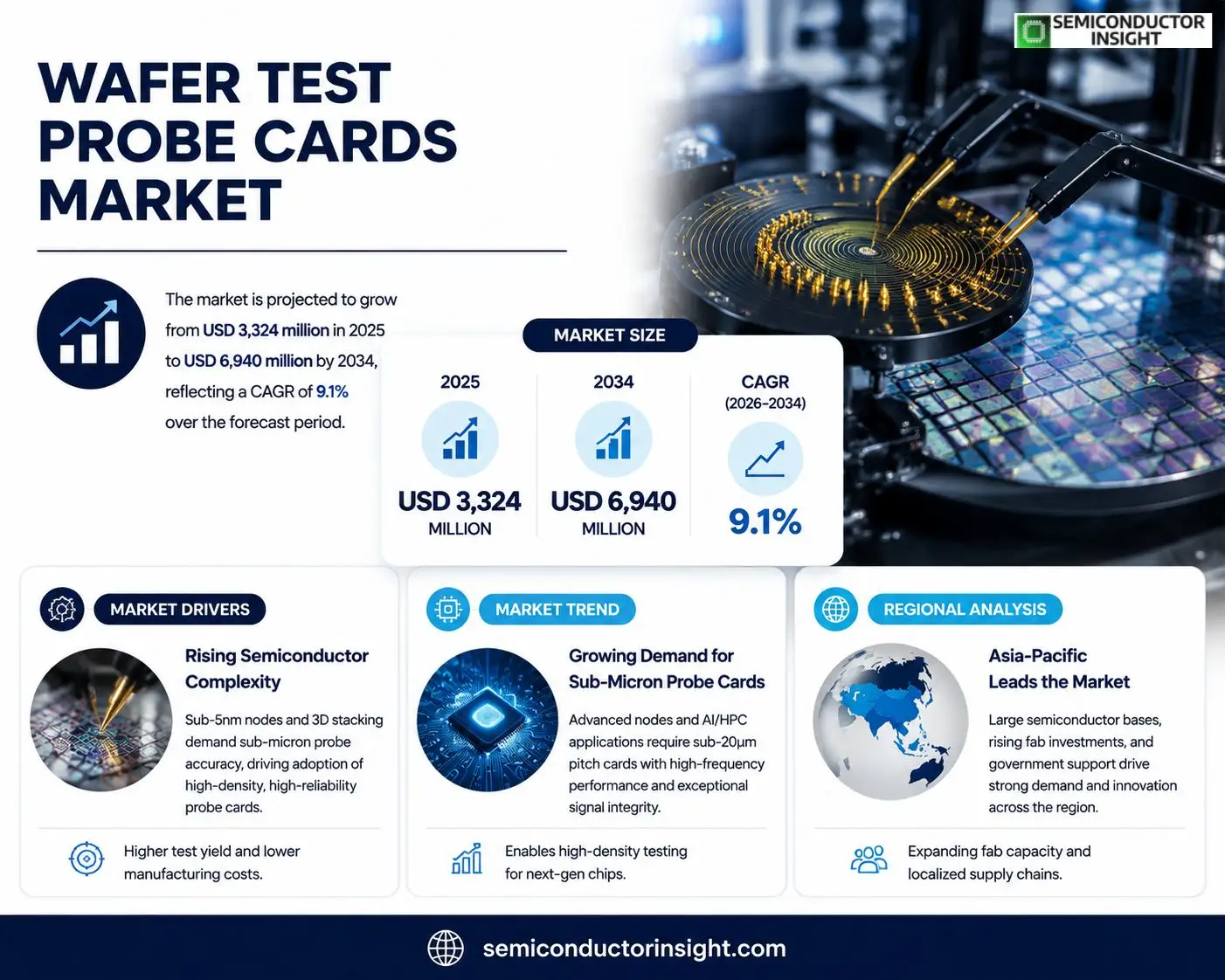
Wafer Test Probe Cards market was valued at USD 3,324 million in 2025 and is expected to climb to USD 6,940 million by 2034, reflecting a compound annual growth rate of 9.1% over the period.
Semiconductor probe cards serve as the essential interface linking test equipment with wafers during chip‑on‑wafer (COW) testing. By contacting each die’s solder pads or bumps through precision probescommonly fabricated from tungsten, rhenium‑tungsten or beryllium copperthe cards convey electrical signals that enable functional and parametric verification before packaging. This screening removes defective dies early, reducing downstream expenses and boosting overall manufacturing yield.
MARKET DRIVERS
Rising Semiconductor Complexity
Designers are embedding more than 10 billion transistors per wafer, forcing test engineers to adopt finer probe tip pitches. Wafer Test Probe Cards Market participants that can deliver sub‑micron contact accuracy gain immediate preference because they reduce false‑fail rates and shorten debug cycles.
Cost‑Efficiency Demands
Manufacturers are squeezing every dollar from the fab floor. A probe card that can handle three test cycles per wafer without re‑qualification cuts tooling expense by roughly 12 %. Vendors that integrate high‑density routing on a single substrate therefore see stronger order volumes.
➤ “Innovators that streamline the probe‑card change‑over process are capturing the upside of tighter production schedules.”
Beyond pure economics, the shift toward heterogeneous integration (e.g., silicon‑photonic and power‑device modules) generates a need for multi‑material probe solutions. Companies that broaden material compatibilitysilicon, gallium nitride, and indium phosphideposition themselves to serve the next wave of mixed‑technology wafers.
MARKET CHALLENGES
Manufacturing Yield Sensitivity
The slightest misalignment of a probe tip can trigger a cascade of yield losses, especially for advanced node wafers under 5 nm. Wafer Test Probe Cards Market firms must invest in sub‑nanometer alignment rigs, a capital outlay that strains smaller players and narrows the competitive field.
Other Challenges
Supply‑Chain Volatility
The semiconductor ecosystem still feels the aftershocks of recent material shortages. Limited access to high‑purity copper and specialty ceramics inflates bill‑of‑materials costs, compelling test‑card manufacturers to renegotiate long‑term contracts or explore alternative alloys.In addition, the escalating regulatory scrutiny on hazardous substances in probe‑card fabrication adds compliance overhead, forcing companies to redesign legacy products to meet evolving standards.
MARKET RESTRAINTS
Regulatory Compliance Overhead
directives such as RoHS and REACH now mandate strict limits on lead, cadmium, and certain flame‑retardants in probe‑card assemblies. Adapting existing lines to satisfy these limits often requires re‑tooling, which can extend time‑to‑market by several months. Smaller manufacturers, lacking the scale to amortize such costs, may lose contracts to larger, compliance‑ready competitors.Furthermore, the growing emphasis on data‑security standards for test‑equipment software introduces another layer of certification. Companies that cannot demonstrate robust cybersecurity controls risk exclusion from OEM supply chains.
MARKET OPPORTUNITIES
Emergence of Advanced Test Architectures
Three‑dimensional (3D) stacked die and fan‑in wafer concepts are creating a fresh demand for probe cards that can access multiple layers without damaging underlying structures. Vendors that engineer flexible interposers and retractable tip arrays stand to capture a sizable share of this nascent segment.Parallel to this, the rise of AI‑driven defect detection tools requires higher‑resolution test data. Probe‑card suppliers that embed on‑board analytics, delivering real‑time signal integrity metrics, will differentiate themselves and command premium pricing.Lastly, emerging markets in Southeast Asia are investing heavily in advanced fabs. Early partnerships with local foundries can lock in long‑term probe‑card supply agreements, expanding Wafer Test Probe Cards Market footprint beyond traditional hubs.
Wafer Test Probe Cards Market Trends
Growing Demand for Sub‑Micron Probe Cards
The shift toward logic nodes below 5 nm and the expansion of 3D‑stacked architectures have forced test engineers to adopt probe cards with sub‑micron pitch. Such cards enable access to increasingly dense bump arrays, allowing manufacturers to separate marginal dies before assembly. Because testing represents a sizable portion of total wafer‑cost, any improvement in pass‑rate translates directly into bottom‑line benefits. Suppliers that can guarantee sub‑20 µm alignment while maintaining signal integrity at high frequencies are seeing stronger order books from foundries focused on AI accelerators and high‑performance compute. The trend is further reinforced by the need to validate thermal‑mechanical‑electrical (TME) reliability in automotive‑grade silicon, where failure‑once‑in‑a‑million is unacceptable.
Other Trends
Material Substitution and Cost Leverage
Historically, probe tips have relied on tungsten or rhenium‑tungsten alloys, which dominate the cost structure. Recent moves toward beryllium‑copper and advanced ceramic substrates are reshaping the supply chain. Domestic production of these alloys reduces exposure to volatile import tariffs and cushions manufacturers against raw‑material price swings. Moreover, the adoption of alumina‑based ceramics improves thermal stability, extending card life in high‑temperature test chambers. Companies that secure in‑house capabilities for alloy casting or partner with local ceramic producers gain bargaining power and can offer more predictable pricing to end‑users, a decisive factor when large‑volume customers negotiate long‑term contracts.
Integration of Test Systems with Advanced Packaging
Modern test stations are no longer stand‑alone platforms; they are engineered alongside probe cards to meet the bandwidth and latency requirements of emerging applications such as 5G/6G front‑ends and edge‑AI modules. Co‑design initiatives focus on matching impedance, minimizing parasitic inductance, and supporting multi‑channel parallel probing that can handle thousands of signals simultaneously. This integration shortens test cycles, reduces equipment footprints, and opens opportunities for vendors that provide both probe hardware and software analytics. For players that fail to align their roadmaps with the evolving packaging ecosystem, the risk is marginalization as customers gravitate toward turnkey solutions that promise faster time‑to‑market and lower total cost of ownership.
COMPETITIVE LANDSCAPEKey Industry Players
Competitive Overview of the Wafer Test Probe Cards Market
The wafer test probe‑card arena is shaped by a handful of multinational OEMs that command the bulk of revenue and pin volume. FormFactor, Technoprobe S.p.A., and Micronics Japan (MJC) together account for more than half of worldwide sales, leveraging deep R&D pipelines and integrated test‑system offerings to satisfy high‑density, sub‑20 µm pitch requirements in advanced logic and HPC applications. Their dominance is reinforced by strategic acquisitions that broaden material portfoliosparticularly in tungsten and beryllium‑copper probe alloysand by long‑term contracts with leading foundries. The market hierarchy therefore resembles a tiered structure: a top tier of vertically integrated giants, a mid‑tier of regional specialists, and a bottom tier of niche innovators that focus on single‑technology cards such as MEMS or vertical probe solutions. Pricing pressure originates from raw‑material volatility, prompting these leaders to pursue cost‑engineering through domestic alloy substitution and automated probe‑placement equipment.Beyond the primary tier, a diverse set of firms sustains competitive intensity by targeting specific segments or geographic corridors. MPI Corporation and MaxOne excel in vertical probe‑card designs for 5 nm and 3D‑IC testing, while SV Probe and CHPT concentrate on high‑frequency MEMS platforms required by 5G/6G and automotive radar. Korean players such as Korea Instrument and Will Technology benefit from proximity to major chip fabs, offering rapid design‑to‑delivery cycles that appeal to local customers. European outfits like Feinmetall and TIPS Messtechnik GmbH differentiate themselves through precision ceramic substrates and bespoke PCB integration. Meanwhile Chinese entrantsincluding Shenzhen DGT, Protec MEMS Technology, and Suzhou Silicon Test Systemare expanding market share by leveraging lower labor costs and aggressive pricing, albeit with varying degrees of quality assurance. This heterogeneous competitive fabric ensures that customers can source bespoke solutions without relying exclusively on the dominant OEMs.
List of Key Wafer Test Probe Cards Companies Profiled
- Technoprobe S.p.A.
- FormFactor
- Micronics Japan (MJC)
- MPI Corporation
- Japan Electronic Materials (JEM)
- MaxOne
- SV Probe
- CHPT
- TSE
- Will Technology
- Korea Instrument
- Feinmetall
- Shenzhen DGT
- Protec MEMS Technology
- Synergie Cad Probe
- Suzhou Silicon Test System
- STAr Technologies, Inc.
- TIPS Messtechnik GmbH
Segment Analysis:
| Segment Category | Sub-Segments | Key Insights |
| By Type |
|
MEMS Probe Card
|
| By Application |
|
Foundry & Logic
|
| By End User |
|
Chip Designers
|
| By Technology |
|
3D
|
| By Sales Channel |
|
Direct Sales
|
Regional Analysis: Wafer Test Probe Cards Market
Asia‑Pacific
Leading fabs are transitioning to sub‑5 nm processes, which impose tighter alignment tolerances on probe cards. This shift forces suppliers to refine micro‑fabrication techniques, creating a niche where only firms with sophisticated lithography capabilities can compete effectively.
National initiatives in China, South Korea, and Taiwan allocate significant funds toward semiconductor test infrastructure. These programs lower entry barriers for new entrants and incentivize existing players to co‑invest in next‑generation probe‑card designs.
The rise of 2.5‑D and 3‑D stacking technologies requires probe cards that can accommodate multiple die‑levels simultaneously. Vendors that pre‑empt this need by offering modular card solutions gain a tactical advantage with high‑volume assemblers.
To mitigate geopolitical risk, many manufacturers are reshoring component sourcing. This trend encourages regional partnerships, reinforcing Asia‑Pacific’s dominance as a hub for both production and innovation in probe‑card technology.
North America
North America remains a strategic market for the Wafer Test Probe Cards sector, primarily because several leading fabless designers operate large test facilities in the United States. The region’s emphasis on high‑performance computing and automotive electronics drives demand for probe cards that can sustain high‑frequency measurements. Moreover, strong intellectual‑property enforcement encourages OEMs to invest in proprietary test solutions, fostering a competitive environment where differentiation is achieved through bespoke engineering services rather than price alone. Companies that can integrate advanced analytics into their test workflows are likely to secure long‑term contracts with key chipset manufacturers.
Europe
European semiconductor hubs, notably in Germany and the Netherlands, prioritize precision manufacturing and low‑defect processes. This focus translates into a preference for probe cards with exceptional mechanical stability and repeatability. Environmental regulations also push vendors toward sustainable materials and energy‑efficient testing equipment. Collaborative consortia across the EU are exploring common standards for probe‑card interfaces, which could streamline cross‑border procurement and reduce time spent on qualification. Firms that align with these standards stand to benefit from a more unified market landscape.
South America
South America’s involvement in Wafer Test Probe Cards Market is currently anchored by a handful of emerging fabs looking to upgrade from legacy 150 mm lines. The region’s growth is constrained by limited capital expenditure, yet the recent influx of foreign direct investment hints at a gradual scaling of production capabilities. Local distributors play a pivotal role in bridging technology gaps, offering after‑sales support and calibration services that are critical for maintaining test accuracy. Suppliers that establish robust service networks can capture nascent demand as the market matures.
Middle East & Africa
The Middle East & Africa region is in the early stages of developing a semiconductor test ecosystem. While most activities are centered on import‑driven consumption, several governments are launching initiatives to build indigenous fab capacity. These programs create a niche for probe‑card vendors able to provide low‑volume, high‑customization solutions that cater to pilot production lines. Partnerships with academic institutions are also emerging, fostering a pipeline of skilled engineers who can support advanced testing methodologies. Early entrants who nurture these relationships may shape the region’s long‑term procurement preferences.
Report Scope
This market research report provides a comprehensive analysis of the Wafer Test Probe Cards Market , covering the forecast period 2026–2034. It offers detailed insights into market dynamics, technological advancements, competitive landscape, and key trends shaping the industry.
Key focus areas of the report include:
- Market Overview: The report begins with an overview outlining its current market scenario, key growth indicators, and industry transformation drivers. It discusses macroeconomic factors, demand–supply balance, regulatory landscape, and the strategic role of semiconductors in powering advancements across industries such as automotive, telecommunications, consumer electronics, and industrial automation.
- Market Size & Forecast: Historical data and future projections for revenue, unit shipments, and market value across major regions and segments.
- Segmentation Analysis: Detailed breakdown by product type, technology, application, and end-user industry to identify high-growth segments and investment opportunities.
- Regional Insights: Insights into market performance across North America, Europe, Asia-Pacific, Latin America, and the Middle East & Africa, including country-level analysis where relevant.
- Competitive Landscape: Profiles of leading market participants, including their product offerings, R&D focus, manufacturing capacity, pricing strategies, and recent developments such as mergers, acquisitions, and partnerships.
- Technology Trends & Innovation: Assessment of emerging technologies, integration of AI/IoT, semiconductor design trends, fabrication techniques, and evolving industry standards.
- Market Drivers & Restraints: Evaluation of factors driving market growth along with challenges, supply chain constraints, regulatory issues, and market-entry barriers.
- Stakeholder Insights: Insights for component suppliers, OEMs, system integrators, investors, and policymakers regarding the evolving ecosystem and strategic opportunities.
Primary and secondary research methods are employed, including interviews with industry experts, data from verified sources, and real-time market intelligence to ensure the accuracy and reliability of the insights presented.
FREQUENTLY ASKED QUESTIONS:
What is the current market size of Wafer Test Probe Cards Market?
-> Wafer Test Probe Cards Market was valued at USD 3324 million in 2025 and is expected to reach USD 6940 million by 2034.
Which key companies operate in Wafer Test Probe Cards Market?
-> Key players include Technoprobe S.p.A., FormFactor, Micronics Japan (MJC), MPI Corporation, Japan Electronic Materials (JEM), MaxOne, SV Probe, CHPT, TSE, Will Technology, Korea Instrument, Feinmetall, Shenzhen DGT, Protec MEMS Technology, Synergie Cad Probe, Suzhou Silicon Test System, STAr Technologies, Inc., TIPS Messtechnik GmbH.
What are the key growth drivers?
-> Key growth drivers include AI and high‑performance computing, automotive electronics, 5G/6G connectivity, Internet of Things proliferation, advanced sub‑5nm processes, 3D packaging, and the need for higher test yield and lower manufacturing costs.
Which region dominates the market?
-> Asia leads Wafer Test Probe Cards Market, driven by large semiconductor manufacturing bases in China, Japan, and South Korea, while Europe and North America remain significant contributors.
What are the emerging trends?
-> Emerging trends include high‑frequency, high‑density testing platforms, MEMS‑based probe cards, material substitution to reduce import dependency, integration of AI‑enabled test analytics, and enhanced reliability designs for automotive‑grade chips.
Get Sample Report PDF for Exclusive Insights
Report Sample Includes
- Table of Contents
- List of Tables & Figures
- Charts, Research Methodology, and more...
 Download Sample Report PDF