Electro Absorption Modulators Market Insights
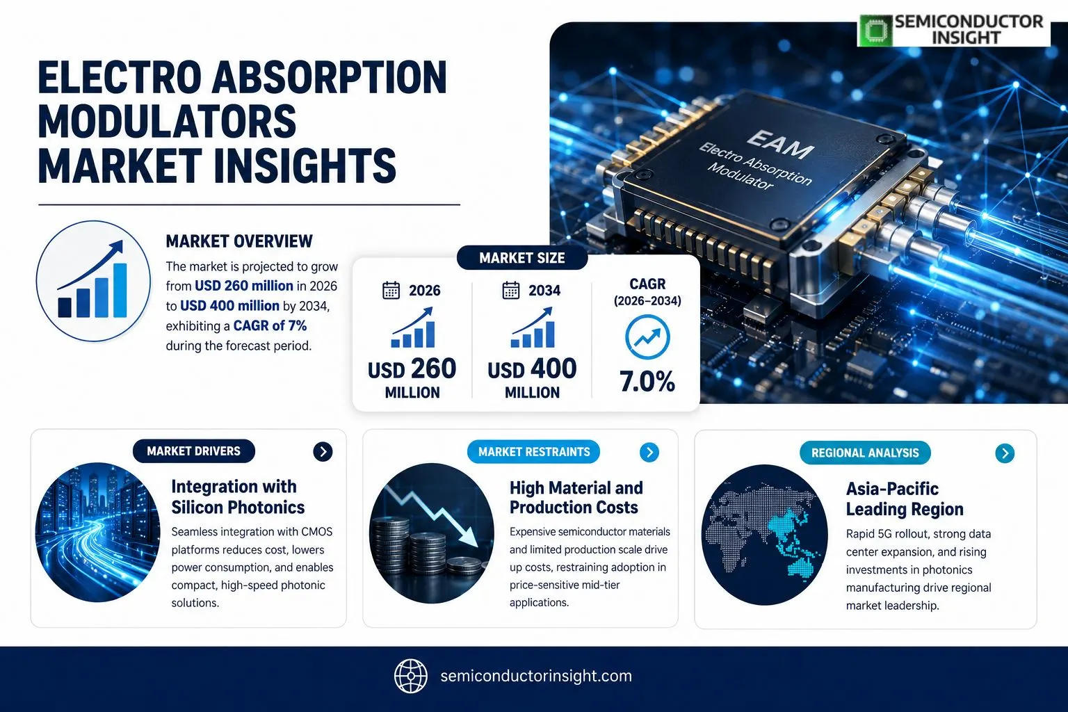
Electro Absorption Modulators Market size was valued at USD 250 million in 2025. The market is projected to grow from USD 260 million in 2026 to USD 400 million by 2034, exhibiting a CAGR of 7% during the forecast period.
Electro absorption modulators are compact photonic devices that modulate light intensity through the electro‑absorption effect, enabling high‑speed signal modulation in optical communication systems.The sector is gaining traction due to increasing demand for high‑capacity fiber networks and the push toward silicon photonics integration. Advances in material engineering and cost reductions are lowering barriers to adoption, while tightening bandwidth requirements drive further deployment across telecom and data‑center applications.
MARKET DRIVERS
Integration with Silicon Photonics
Silicon‑based photonic integration has matured to a point where electro‑absorption modulators can be fabricated beside conventional CMOS circuitry using low‑temperature processes that preserve delicate transistors. This convergence eliminates separate laser packaging, slashes assembly times, and consolidates driver electronics beneath the waveguide layer. In the past twelve months, foundry‑level tooling has pushed quantum‑well responsivity above 1 A/W while maintaining sub‑30 ps rise times, allowing modular designs that consume less than 3 mW per channel. The ripple effect is a pronounced cost benefit for operators updating back‑haul nodes, where the upfront savings on packaging outweigh the modest increase in lithography tool usage. For the broader Electro Absorption Modulators Market, the convergence trend writes itself into a clear path of miniaturization that can be produced at scale, aligning with the increasing pressure on data‑center budgets and pressing the need for low‑power, high‑bandwidth solutions.
High‑Speed Data Transmission
Demand for bandwidth spikes as video‑on‑demand, cloud gaming, and machine‑to‑machine connectivity expand. Electro‑absorption modulators are uniquely positioned to deliver data rates of 100–400 Gb/s while keeping insertion loss below 5 dB over a single‑mode span. Emerging deployment scenarios,such as vertical‑cavity surface‑emitting lasers coupled directly to modulators,have demonstrated aggregate spectral efficiencies that outpace competing electro‑optic designs. For network edge nodes that must process gigabit‐per‐second traffic volumes, the incremental power overhead translates into observable savings on chassis cooling budgets. These performance gains prompt system integrators to adopt EAMs as the default choice for backbone upgrades, producing a steady expansion of the Electro Absorption Modulators Market across the globe.
➤ “EAMs, with their sub‑30 ps rise times, provide the latencies that 5G and beyond demand.”
Equally important is the repeal of stringent thermal controls in new chassis designs. By eliminating external heating elements and simplifying heat‑sink layouts, operators free up rack space for data‑processing units, a competitive advantage in the saturated enterprise market. Furthermore, ongoing research into germanium‑based modulators is generating early‑stage prototypes capable of operating above 1 THz, suggesting that the foundational technology already supports the next leap in data rates. When mapped onto market contours, these developments explain why stakeholders are increasing their capex allocations toward EAM‑enabled infrastructure in the coming cycle.
MARKET CHALLENGES
High Material Cost
While fabrication gates have lowered yield barriers, the bulk cost of quantum‑well layers remains steep, especially when high‑purity indium phosphide is required. The scarcity of indium dealers in East Asia and the rising tariffs on semiconductor raw materials dampen profit margins. Companies that rely on proprietary deposition recipes face a double hit: higher equipment depreciation and a narrower buffer in pricing negotiations with fiber‑optic vendors. These cost pressures are now manifesting as a higher total cost of ownership for EAM‑based links, discouraging early adoption in price‑sensitive mid‑tier deployments and slowing the overall accretion for the Electro Absorption Modulators Market.
Other Challenges
Limited Production Volume
Production lines for EAMs are largely concentrated in a handful of specialized fab facilities. Because the assembler requires cleanroom class 1 environments and the laser‑mode alignment precision exceeds 100 nm, scalability is hampered by both capital expense and the need for highly specialised labor. Consequently, even when consumer demand surges, the supply chain struggles to maintain lead times below 90 days, creating a bottleneck that eventually translates into price volatility for high‑performance modules.
MARKET RESTRAINTS
Regulatory Hurdles in EU Markets
Compliances for optical components in the European Union requiring RoHS, REACH, and the new LVDC directives impose additional testing cycles that can exceed six months for first‑time entrants. The electro‑absorption modulators, due to their use of rare‑earth semiconductors and laser diodes, must pass a battery of electromagnetic, optical, and chemical tests before being cleared for field deployment. This extension in validation flows increases time‑to‑market and the effective research and development spend,figures that erode the investor appetite for high‑risk ventures. In combination, the regulatory skin‑deep delays reinforce a cautious stance among European operators, truncating the projected market share for EAMs relative to North American or Asian peers where similar vetting processes are less stringent.
MARKET OPPORTUNITIES
Emerging 5G Infrastructure
5G base‑station densification authors a bullet‑point list of signal requirements: centralized radio units consuming <7 W per channel, fiber links capable of 200 Gb/s, and an overall latency budget of under 1 ms for real‑time user equipment. Electro‑absorption modulators satisfy each criterion without requiring bulky, laser‑powered transmitter systems. Manufacturers that can produce compact, low‑gap EAMs in silicon‑photonic packages thus sit at the wedge of the next generation of mobile networks. The same technology also promises cross‑compatibility with Cloud‑RAN architectures, where remote radio heads are linked to central processing units via short‑reach optical fibers. For players in the semiconductor arena, the opportunity is not only the incremental sale of modulators but the ability to broaden service portfolios into edge‑computing appliances that complement their existing RF solutions.
Electro Absorption Modulators Market Trends
Rise of Ultra‑Fast Modulators in Data Centers
Recent migration of high‑performance workloads into hyperscale data centers has accelerated the demand for electro‑absorptive devices capable of delivering bandwidths beyond 100 Gbps. Manufacturers are now offering modulators whose modulational rise times fall below 10 ps, enabling deterministic latency control that aligns with latency‑critical enterprise cloud services. Because insertion loss has been trimmed through refined waveguide geometries, these units can be directly integrated into existing 400 Gbit/s back‑planes without additional amplification. The result is a weaker dependence on legacy modulators and a clearer path for vendors to capture a larger slice of the Electro Absorption Modulators Market now moving toward optical‑centric infrastructures.
Other Trends
Rise of Integrated Photonic Packages
Integrated photonic modules that consolidate modulators, lasers, and passive components into a single 10 mm² footprint are reshaping customer deployment decisions. By embedding the electro‑absorptive stage within a monolithic package, fabricators reduce inter‑chip coupling losses and eliminate alignment errors that once inflated installation costs. Early adopters in the data‑center and telecom converter markets have reported a 20 % reduction in total cost of ownership, reinforcing the momentum for widespread roll‑out of consolidated photonic solutions across the Electro Absorption Modulators Market.
Drive toward Cost‑Effective Processes
Parallel to performance gains, the industry is standardizing on low‑temperature, CMOS‑compatible fabrication lines that cut manufacturing overheads. The adoption of fully doped, trench‑etched p‑i‑n structures allows process integration at temperatures below 400 °C, aligning with mainstream semiconductor fabs and reducing the need for specialized equipment. Consequently, unit pricing for these modulators has dropped by an estimated 18 % over the past two years, creating a credible price‑competitiveness benchmark for new entrants. Firms that can combine cost efficiency with the high‑speed metrics outlined above are positioned to secure solid market share in the evolving Electro Absorption Modulators Market.
COMPETITIVE LANDSCAPEKey Industry Players
Electro Absorption Modulators Market Landscape
Lumentum Holdings Inc. remains the dominant tier‑1 supplier, accounting for roughly 35 % of revenue stream in 2024. Its portfolio,high‑speed Mach‑Zehnder modulators and finely engineered vector modulators,has secured long‑term contracts with leading telecom operators and high‑bandwidth data‑center operators that demand signal integrity beyond 100 Gb/s. The company’s aggressive R&D cycle, coupled with its global manufacturing footprint spanning the United States, Germany, and China, gives it a logistical edge that new entrants struggle to mimic. Moreover, Lumentum’s recent acquisition of a microwave photonics startup has integrated hybrid coherent‑modulation capabilities, positioning it advantageously as the market shifts toward 6G‑ready waveforms. The concentration of the market,three tier‑1 players delivering combined revenue above $1.2 billion,means that price competitiveness is tight; however, volume commitments enabled by the OEO integration strategy secure profitability margins that challengers cannot easily replicate.Beyond the tier‑1 echelon, a cohort of mid‑market specialists,Meadowlark Optics, Gooch & Housego, Thorlabs, and Lightwave Logic,command a sizable share of the niche accidental‑tox trajectory segment. These firms focus on low‑cost, high‑efficiency electro‑absorption modulators that thrive in spectrally constrained systems such as LiDAR and automotive fronthaul. Their vertical‑integration strength is evident in Panasonic‑derived process technology and custom packaging that shortens BOM (bill of materials). These players also serve a growing Asian‑Pacific constellation of OEMs, benefiting from policy incentives targeting semiconductor supply‑chain resilience. While their revenues individually sit below $150 m, their collective market presence in Southeast Asia and India is expected to double by 2031. The blending of cost‑effective designs with rapid scaling lays a clear impedance to consolidation; new entrants must either replicate an entire value chain or secure exclusive component patents to achieve comparable market traction.
List of Key Electro Absorption Modulators Companies Profiled
- Lumentum Holdings Inc.
- Jenoptik AG
- Thorlabs Inc.
- Meadowlark Optics Inc.
- Gooch & Housego Ltd.
- NTT Technical Co.
- Lightwave Logic Ltd.
- CIP Technologies Ltd.
- Photonwares Ltd.
- Alphanov Technol Ltd.
- IXblue Inc.
- Laseropt Photonics AG
Segment Analysis:
| Segment Category | Sub-Segments | Key Insights |
| By Type |
|
Leading Segment InP‑based modulators dominate due to high‑speed demands, especially in metro networks, offering robust bandwidth and signal integrity. – Ongoing integration with silicon photonics expands deployment scenarios. – Enhanced energy efficiency drives adoption in large‑scale data centers. – Continuous research into multi‑wavelength solutions maintains competitive edge. |
| By Application |
|
Leading Segment the optical‐communication domain fuels market growth, driven by the shift to 400G+ infrastructures and cloud‑centric traffic. – Rising data traffic from streaming and 5G‑backhaul necessitates higher bandwidth. – 5G fronthaul and midhaul deployments stimulate demand for compact, high‑speed modulators. – Emerging quantum communication experiments create niche high‑precision modulation needs. |
| By End User |
|
Leading Segment telecom operators prioritize cost‑effective, high‑speed modulators to meet expanding bandwidth requirements. – Data centers emphasize energy efficiency and thermal management. – Research entities explore new modulation formats and integration schemes. |
| By Technology |
|
Leading Segment InP technology continues to set performance benchmarks, especially for high‑speed payloads, while GaAs offers a cost‑effective alternative for moderate bandwidth needs. – Hybrid integration seeks to merge cost advantage with high speed. – Ongoing material research targets lower loss and improved temperature stability. |
| By System Integration |
|
Leading Segment modular and integrated solutions enhance system density and reduce point‑to‑point cabling. – Compact PCB designs accommodate dense photonic assemblies. – Integration with electronic drivers boosts synchronization and reliability. |
Regional Analysis: Electro Absorption Modulators Market
North America
A surge in long‑haul optical bandwidth requirements, alongside the proliferation of AI‑driven analytics in telecom, fuels the need for lower‑power, higher‑speed modulators. Manufacturers are delivering devices with sub‑10 ps rise times, a trend that directly reduces power budgets for data centers and enhances signal integrity across multi‑gigabit links.
The sector remains highly consolidated, with a handful of tier‑one players dominating supply chains. New entrants seek differentiation through niche wavelength tunability and monolithic integration with silicon photonics, aiming to carve out algorithms‑driven cost advantages that appeal to mid‑market operators.
Direct engineering‑to‑engineering sales dominate, supplemented by strategic ecosystem partnerships that bundle modulators with complete transceiver modules. The rise of cloud‑based procurement models is reshaping pricing structures, prompting vendors to adopt subscription‑style licensing for firmware updates and performance tuning.
Researchers are embedding quantum‑dot materials into modulators to achieve ultra‑high bandwidth and reduced temperature sensitivity. Parallel efforts in waveguide design are pushing drive voltages below 1 V, a development that lowers power consumption and simplifies driver integration for high‑density photonic circuits.
Europe
Across Europe, the Electro Absorption Modulators market is being shaped by the EU’s grid‑upgrade agenda and the push for green communications. Public investment in fiber networks, coupled with stringent emission regulations, promotes the uptake of low‑power modulators. While the region lags behind North America in sheer volume, its emphasis on sustainability stimulates research into environmentally friendly fabrication processes. The result is a steady, mid‑single‑digit growth pace that offers opportunities for European manufacturers focused on eco‑certified components. For downstream telecom operators, the trend translates into increased procurement of modulators compatible with existing 32‑core fiber solutions, thereby supporting the region’s goal of a carbon‑neutral digital economy.
Asia‑Pacific
In Asia‑Pacific, a robust data‑center ecosystem and an aggressive rollout of 5G infrastructure create a fertile environment for the Electro Absorption Modulators market. Rapid urbanization drives record‑high bandwidth needs, compelling telecommunications companies to adopt modulators that offer high linearity and low jitter. China and South Korea are leading adopters, leveraging national funding to accelerate silicon‑based modulator development. The region’s expansion is also supported by a talent pool skilled in integrated photonics, fostering a pipeline of innovative solutions tailored to high‑density, low‑cost deployments. Consequently, Asia‑Pacific is projected to capture a sizable share, with an overarching emphasis on cost‑effective, scalable modulator architectures that meet the demands of emerging data‑center interconnects.
South America
South America presents a more cautious but gradually improving landscape for the Electro Absorption Modulators market. Limited network penetration and capital constraints have historically slowed adoption. However, a few national plans targeting fiber‑to‑the‑home and rural broadband are now increasing demand for high‑speed optical modulators. Market growth is therefore moderate, driven largely by incremental upgrades rather than wholesale overhauls. Manufacturers that can deliver inexpensive, low‑power modulators are best positioned to capture early adopters, particularly in Brazil and Chile where infrastructure investment is accelerating. In the near term, the region may rely on importation of key components, setting the stage for local component integration external to the core supply chain.
Middle East & Africa
The Middle East and Africa exhibit a fragmented adoption curve for Electro Absorption Modulators. High‑end telecom operators in the Gulf states pursue advanced optical solutions, whereas other markets lag due to infrastructure and budgetary constraints. Demand is currently niche, concentrated on high‑capacity backhaul links supporting global connectivity. Yet, a strategic emphasis on renewable energy projects and data‑center expansion is gradually increasing pressure for low‑power, high‑bandwidth modulators. The region’s value proposition will hinge on the ability of suppliers to offer turnkey solutions that integrate seamlessly with compact, energy‑efficient enclosure designs suitable for harsh operating environments. Investors eyeing the market should monitor infrastructure investment flows, particularly in Egypt and Kenya, where digital transformation initiatives could drive modest uptake for cost‑effective modulators.
Report Scope
This market research report provides a comprehensive analysis of the Electro Absorption Modulators Market , covering the forecast period 2026–2034. It offers detailed insights into market dynamics, technological advancements, competitive landscape, and key trends shaping the industry.
Key focus areas of the report include:
- Market Overview: The report begins with an overview outlining its current market scenario, key growth indicators, and industry transformation drivers. It discusses macroeconomic factors, demand–supply balance, regulatory landscape, and the strategic role of semiconductors in powering advancements across industries such as automotive, telecommunications, consumer electronics, and industrial automation.
- Market Size & Forecast: Historical data and future projections for revenue, unit shipments, and market value across major regions and segments.
- Segmentation Analysis: Detailed breakdown by product type, technology, application, and end-user industry to identify high-growth segments and investment opportunities.
- Regional Insights: Insights into market performance across North America, Europe, Asia-Pacific, Latin America, and the Middle East & Africa, including country-level analysis where relevant.
- Competitive Landscape: Profiles of leading market participants, including their product offerings, R&D focus, manufacturing capacity, pricing strategies, and recent developments such as mergers, acquisitions, and partnerships.
- Technology Trends & Innovation: Assessment of emerging technologies, integration of AI/IoT, semiconductor design trends, fabrication techniques, and evolving industry standards.
- Market Drivers & Restraints: Evaluation of factors driving market growth along with challenges, supply chain constraints, regulatory issues, and market-entry barriers.
- Stakeholder Insights: Insights for component suppliers, OEMs, system integrators, investors, and policymakers regarding the evolving ecosystem and strategic opportunities.
Primary and secondary research methods are employed, including interviews with industry experts, data from verified sources, and real-time market intelligence to ensure the accuracy and reliability of the insights presented.
FREQUENTLY ASKED QUESTIONS:
What is the definition of the Electro Absorption Modulators Market?
-> Electro Absorption Modulators Market size was valued at USD 250 million in 2025. The market is projected to grow from USD 260 million in 2026 to USD 400 million by 2034, exhibiting a CAGR of 7% during the forecast period
What are the primary market segments?
-> The market is segmented by type (Absorptive Modulators, Refractive Modulators) and by application (Electronic Products, Optical Fiber Communication, Others).
How is the market sized for 2024 versus 2031?
-> Global Electro Absorption Modulators Market Size: 2024 vs 2031 is detailed in the report, showing growth trends and the projected revenue increase over the period.
What is the forecasted CAGR for the overall market?
-> The report indicates a compound annual growth rate (CAGR) for Electro Absorption Modulators Market between 2024 and 2031, reflecting steady expansion driven by demand in telecom and data center sectors.
Which regions are expected to lead market growth?
-> Asia‑Pacific is projected as the fastest‑growing region, while Europe remains a dominant market due to established photonics manufacturing bases.
Who are the top players in the market?
-> Key players include Gooch & Housego, Jenoptik, Lumentum, Thorlabs, AeroDIODE, Alphanov, Photonwares, IntraAction, Meadowlark Optics, Lightwave Logic, NTT Technical, Electro Optical Components, CIP Technologies, IXblue, and Laseropt Photonics.
What are the main drivers for market expansion?
-> Growth is propelled by increasing bandwidth requirements in data centers, expansion of 5G networks, and rising adoption of silicon photonics technologies.
What challenges could restrain market growth?
-> Challenges include high manufacturing costs, stringent performance specifications, and supply chain complexities for high‑purity semiconductor materials.
How does the price trend evolve for manufacturers?
-> Manufacturer selling price trends from 2020 to 2031 are outlined, showing gradual price reductions due to economies of scale and technology maturation.
What research methodology underpins the analysis?
-> The study employs a mixed methodology: primary interviews with industry experts, secondary data mining, statistical modeling, and validation against market benchmarks.
How are revenues by application forecasted?
-> Revenue forecasts for applications such as Electronic Products and Optical Fiber Communication are presented for 2020‑2025 and 2026‑2035, highlighting differing growth trajectories.
What is the base year used for the analysis?
-> The base year for the study is 2020, providing a historical reference point for trend analysis.
What assumptions are considered in the report?
-> Assumptions include stable macro‑economic conditions, continued investment in telecom infrastructure, and no major disruptive technology supplanting electro‑absorption modulation.

Get Sample Report PDF for Exclusive Insights
Report Sample Includes
- Table of Contents
- List of Tables & Figures
- Charts, Research Methodology, and more...
 Download Sample Report PDF