
Key Statistics
Key Takeaways
- 6-inch substrates are the leading size segment in the source page because larger wafers can increase device output per process cycle and lower unit processing cost, although maintaining crystal quality and yield at large diameters remains technically difficult.
- Optical module devices are the largest application because InP’s direct bandgap and high electron mobility support lasers, photodetectors and modulators operating at telecom wavelengths used in high-speed fiber networks and AI data-center interconnects.
- Asia Pacific is the largest regional market, supported by major substrate producers in Japan and China and by semiconductor and optical-module manufacturing across Japan, China and South Korea.
- Capacity investment accelerated in 2026: JX Advanced Metals announced a policy for up to JPY 120 billion of InP substrate investment over four years, while AXT raised capital to expand InP capacity and signed a long-term supply and capacity-reservation agreement with Lumentum.
- Indium availability remains a strategic supply issue. USGS reported no U.S. mine recovery of indium in 2025 and estimated refined-indium prices around USD 350,000 per metric ton, reinforcing the importance of upstream sourcing and material efficiency.
InP Substrate Market Overview
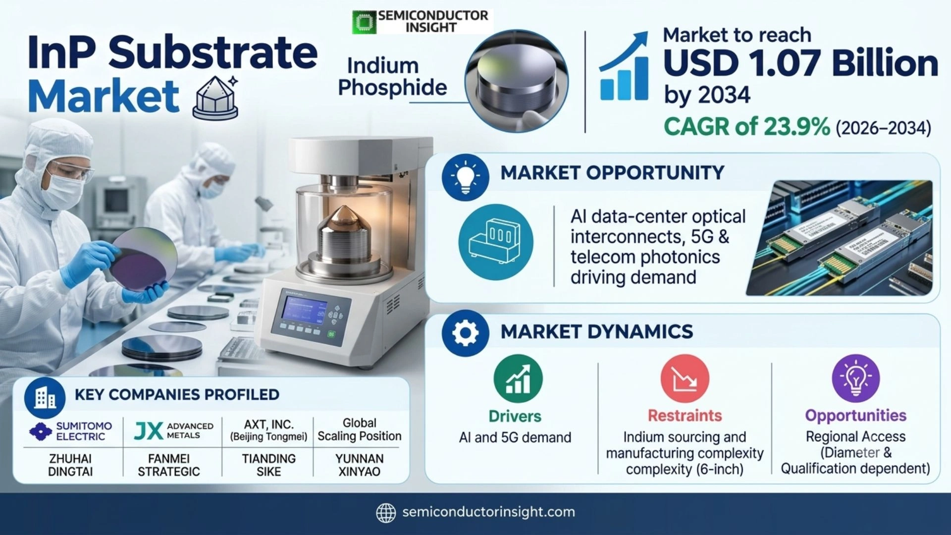
InP substrate market is valued at USD 155 million in 2025, rises to an estimated USD 192 million in 2026, and is projected to reach USD 1.07 billion by 2034. The two published size anchors imply a 23.9% CAGR during 2026–2034. Asia Pacific is the largest region because Japan and China combine established substrate suppliers with dense optical-component manufacturing, while optical module devices are the leading application and the source page identifies 6-inch wafers as the leading size segment.
Indium phosphide substrates are single-crystal III-V semiconductor wafers used as the foundation for epitaxial layers and devices that require direct-bandgap optical performance or very high electron mobility. InP is particularly important for lasers, photodetectors and modulators in fiber-optic communications, as well as selected high-frequency electronics and infrared sensing. The substrate must provide low defect density, controlled electrical properties, precise orientation and a surface suitable for epitaxial growth.
The market is increasingly tied to AI data-center optics. JX Advanced Metals states that InP substrates are used in optical transceivers that support the large-volume data transmission required by AI, and in June 2026 it announced an investment policy of up to JPY 120 billion over four years to strengthen production. AXT likewise describes InP as a key material for high-speed optical data transmission and is expanding capacity, showing that demand is moving from a niche material cycle toward strategic infrastructure supply.
Substrate scaling is difficult because compound-semiconductor crystal growth does not follow the same economics as mature silicon wafers. Larger diameters improve device-fab productivity, but dislocations, microcracks, dopant uniformity and wafer flatness become harder to control. Sumitomo Electric has published work on 6-inch InP crystal growth, while AXT now lists 2-, 3-, 4- and 6-inch InP products. This makes diameter expansion a competitive capability rather than simply a catalog extension.
Segment Analysis: By Type
By type, the source page segments the market into 2-inch, 3-inch, 4-inch, 6-inch, and Other substrates. The source identifies 6-inch wafers as the leading segment because larger diameter can improve manufacturing efficiency for high-volume optical and RF devices. Smaller wafers remain important for research, specialty products and production lines where equipment and epitaxial processes are already qualified around legacy diameters.
| Type | Technical / commercial role | Market position |
|---|---|---|
| 2-inch | Two-inch InP remains relevant for research, specialty photonics, infrared devices and mature production where equipment is optimized around smaller wafers. The lower absolute wafer cost and broad availability make it useful for low-volume development, but device throughput per processing step is much lower than on larger diameters, limiting its economics for rapidly growing AI optical-module demand. | Mature niche segment. Demand persists because many device structures and research lines do not justify conversion, but long-term share is pressured as optical-component manufacturers seek larger wafers to improve throughput. Suppliers compete on crystal quality, dopant variety and small-lot flexibility rather than volume efficiency. |
| 3-inch | Three-inch wafers provide an intermediate format used in established compound-semiconductor production. They can support optical and RF devices with lower equipment-transition risk than moving directly to 6 inches, and they remain relevant where customer process tools, epitaxy reactors and lithography are qualified around this diameter. | Stable legacy-production segment. Its commercial position depends on installed equipment and long device lifecycles, but it is less attractive for new high-volume AI optical manufacturing because the wafer area does not deliver the same economies as 4- or 6-inch substrates. |
| 4-inch | Four-inch InP is widely used in optical communications and provides a practical balance between wafer area, crystal quality and equipment availability. JX Advanced Metals lists 2-, 3- and 4-inch InP products, and Sumitomo Electric highlights 4-inch wafers in its current optical-device technology content. The diameter supports established volume production without the full technical risk of 6-inch crystal scaling. | Large established commercial segment. Four-inch is important for current optical transceiver and photonic device supply because many epi and device processes are already qualified. It may remain a high-volume workhorse even as 6-inch investment grows, particularly when device makers value proven yield over theoretical wafer-area efficiency. |
| 6-inch | Six-inch wafers expand usable area and can reduce processing cost per device when crystal and device yields are maintained. The source page identifies this diameter as leading, and AXT currently lists 6-inch InP availability. Sumitomo Electric has documented crystal-growth and wafer-processing challenges at 6 inches, underscoring that scale requires tight control of dislocations, thermal stress and polishing. | Leading and fastest strategic segment. AI optical interconnect demand creates a strong incentive to increase wafer output per fab cycle, but suppliers must prove uniformity and yield before customers convert. Companies that achieve stable 6-inch volume can gain share because device manufacturers can increase throughput without proportionally expanding epitaxy and lithography tools. |
| Other | Other diameters and custom substrate formats serve specialized research, infrared sensing, quantum photonics and engineering requirements. These products may use unusual orientation, doping or thickness specifications and are often sold in lower volumes. Supplier value comes from flexibility and material science rather than manufacturing scale. | Small but defensible segment. Custom wafers can carry higher value per piece because customers need specific electrical or crystallographic properties. Growth is tied to emerging photonic and sensing applications rather than mainstream optical-module volume. |
Why is 6-inch InP strategically important but technically difficult?
A 6-inch wafer provides more device area per epitaxy and lithography cycle, which can reduce cost per laser or detector when yields remain high. The difficulty is maintaining uniform crystal quality across the larger diameter. Thermal gradients, dislocations and mechanical stress become harder to manage during crystal growth and wafer processing. The market therefore rewards suppliers that can scale diameter without sacrificing defect density, flatness, dopant uniformity or surface quality.
Segment Analysis: By Application
By application, the source page segments the market into Optical Module Devices, RF Devices, Sensor Devices, and Other Applications. Optical module devices hold the largest share because InP is well suited to 1.3 µm and 1.55 µm communication wavelengths used for lasers, photodetectors and modulators. RF devices and sensors use the material where high electron mobility, high-frequency performance or infrared response justify its higher cost compared with silicon or GaAs.
| Application | Demand characteristics |
|---|---|
| Optical Module Devices | This is the largest application because data-center and telecom optical modules require efficient light generation and detection at fiber-communication wavelengths. InP substrates support lasers, electro-absorption devices, photodetectors and photonic integrated circuits. AI infrastructure is strengthening demand because faster optical transceivers need more laser and detector content, turning substrate availability and large-diameter yield into strategic capacity issues for the optical supply chain. |
| RF Devices | InP can support very high electron velocity and high-frequency operation, making it relevant for selected HEMT, HBT and millimeter-wave devices used in telecom, satellite and defense systems. Volumes are smaller than optical communications, but performance requirements are stringent and device value is high. Customers prioritize semi-insulating substrate quality, dopant control, reliability and long-term material availability. |
| Sensor Devices | Infrared detectors, LiDAR-related photonics and specialized sensing can use InP substrates where direct-bandgap optical properties or high-speed response are valuable. Demand is fragmented across industrial, automotive, scientific and defense applications, so suppliers must provide multiple dopants, orientations and diameters. These applications can support premium pricing but rarely match optical-module shipment volumes. |
| Other Applications | Quantum photonics, integrated photonic circuits, research devices and specialized optoelectronics form a smaller but strategically interesting application pool. InP is attractive because it supports active optical functions that silicon alone cannot provide efficiently. The opportunity is strongest where heterogeneous integration combines InP light sources with silicon photonics or other platforms, creating new demand for high-quality starting substrates and transfer processes. |
Regional Analysis
Asia Pacific dominates the InP substrate market because the region combines leading substrate manufacturers, optical-component production and semiconductor supply chains. Japan hosts Sumitomo Electric and JX Advanced Metals, China hosts AXT/Tongmei and several emerging suppliers, and South Korea has strong RF and optical-device demand. North America and Europe focus more on high-value photonics, aerospace, quantum and research applications than on substrate volume.
Why does Asia Pacific hold the largest share of InP substrate demand and production?
Compound-semiconductor materials benefit from geographic clustering because substrate growth, epitaxy, optical-device fabrication and module assembly are tightly linked by qualification and logistics. Asia Pacific has the strongest cluster across these stages. Japan contributes established high-quality crystal growth, China is expanding domestic capacity aggressively, and regional optical-module manufacturing creates nearby demand. North America and Europe remain strategically important but rely more heavily on imported substrate volume.
| Region | Position | Growth outlook | Demand profile | What decides supplier selection |
|---|---|---|---|---|
| Asia Pacific | Largest | Highest | Production and optical-module led | Crystal quality, diameter scale, local capacity and qualification |
| North America | High-value market | High | AI optics, defense, research and sensing-led | High performance, secure supply and technical support |
| Europe | Specialty market | Moderate to high | Photonics, telecom, automotive and research-led | Quality, traceability and specialized specifications |
| South America | Small | Low to moderate | Research and specialty import-led | Availability, small-lot supply and landed cost |
| Middle East & Africa | Emerging | Moderate from small base | Telecom, satellite and research-led | Partnerships, imported supply and technical support |
Competitive Landscape
The market is moderately consolidated around companies that have proprietary crystal-growth know-how, raw-material access and long customer qualifications. The source page profiles Sumitomo Electric Industries, JX Advanced Metals Corporation, Beijing Tongmei Xtal Technology (AXT), Zhuhai Dingtai Xinyuan, FanMei Strategic Metal Resources, Guangdong Tianding Sike New Materials and Yunnan Xinyao Semiconductor Materials. Competition is intensifying as AI optical demand makes capacity and larger diameters more valuable.
Japanese suppliers have long-standing positions in high-quality compound-semiconductor substrates. JX Advanced Metals currently offers 2-, 3- and 4-inch InP and states that its products serve optical modules, mobile base stations and data centers. Its 2026 plan for up to JPY 120 billion of additional investment shows how established suppliers are responding to AI optical demand. Sumitomo Electric also emphasizes strengthening InP substrate production capacity and has technical experience with 6-inch crystal growth.
AXT is becoming a major capacity challenger. The company lists InP in 2-, 3-, 4- and 6-inch diameters and identifies AI data-center interconnects, co-packaged optics and silicon photonics among target applications. In April 2026 it raised gross proceeds of about USD 550 million to support Tongmei InP capacity and R&D, and in July signed a long-term capacity-reservation agreement with Lumentum extending through 2031.
Chinese specialty-material suppliers benefit from domestic semiconductor and optical-component demand, but moving from smaller diameters into high-quality 6-inch substrates requires sustained investment in crystal growth, wafer processing and customer qualification. Competitive advantage therefore depends on yield and quality rather than nominal capacity alone. As demand accelerates, customers are likely to secure long-term agreements and deposits to reserve qualified substrate capacity rather than rely on spot procurement.
| Competitive tier | Companies | Why they matter |
|---|---|---|
| Established global leaders | Sumitomo Electric Industries; JX Advanced Metals Corporation | These Japanese suppliers have mature crystal-growth and wafer-processing technology, established optical-communications customers and broad quality credentials. Their advantage is the ability to support demanding device makers with consistent substrates and long-term technical relationships. Current investment programs indicate that they are defending leadership through capacity expansion rather than relying only on existing qualified lines. |
| Scaling international challenger | Beijing Tongmei Xtal Technology / AXT | AXT combines proprietary Vertical Gradient Freeze crystal growth, a multi-diameter InP portfolio and a vertically connected raw-material network in China. Its 2026 capital raise, 6-inch R&D and long-term supply agreement with Lumentum show that it is scaling specifically for AI optical demand, making capacity availability a central competitive differentiator. |
| Regional Chinese suppliers | Zhuhai Dingtai Xinyuan; FanMei Strategic Metal Resources; Guangdong Tianding Sike New Materials; Yunnan Xinyao Semiconductor Materials | These companies participate in China’s compound-semiconductor localization push and can benefit from domestic optical and RF demand. Their growth opportunity depends on proving defect control, large-diameter capability and consistent qualification. Regional customer proximity and policy support are advantages, but high-end optical users still require performance comparable with established Japanese and international suppliers. |
Companies profiled in the report
The source page profiles Sumitomo Electric Industries, JX Advanced Metals Corporation, Beijing Tongmei Xtal Technology (AXT), Zhuhai Dingtai Xinyuan, FanMei Strategic Metal Resources, Guangdong Tianding Sike New Materials, and Yunnan Xinyao Semiconductor Materials. The report scope retains this complete list. Competitive analysis separates established global suppliers from AXT’s scaling position and from regional Chinese companies whose market access depends on larger-diameter capability and high-end customer qualification.
Production Capacity Analysis
Production capacity is constrained by high-purity indium and phosphorus feedstock, single-crystal growth yield, wafer machining and customer qualification. Unlike commodity silicon, InP volumes are smaller and the crystal-growth process is technically demanding. Larger diameters amplify thermal and defect-control challenges, so announced capacity does not become interchangeable supply until the resulting wafers meet customer specifications for dislocation density, resistivity, flatness, surface quality and dopant uniformity.
Raw-material supply is strategically important because indium is largely recovered as a byproduct of zinc and other metal processing rather than mined as a primary commodity. USGS reported no U.S. recovery of indium from ores in 2025 and estimated refined-indium prices at roughly USD 350,000 per metric ton. Substrate producers therefore manage exposure through inventory, recycling where feasible, long-term sourcing and upstream relationships rather than assuming unlimited spot-market availability.
Crystal growth is the core technical bottleneck. InP is formed from indium and phosphorus under tightly controlled high-temperature conditions, and large single crystals must maintain electrical and structural uniformity. Sumitomo Electric describes crystal-growth temperatures above 1,000°C and has published work on 6-inch InP processing. As diameter rises, dislocations and thermal stress become more difficult to control, which makes usable yield more important than nominal crystal-puller throughput.
Wafer processing converts crystals into flat, polished substrates through slicing, lapping, edge shaping, etching, polishing and cleaning. Customers qualify specific diameters, orientations, dopants and supplier sites for epitaxy. JX currently lists 2-, 3- and 4-inch commercial products, while AXT lists up to 6 inches. This difference illustrates why capacity must be evaluated by qualified product mix rather than total wafer count.
Investment is accelerating faster than in previous cycles because AI optics creates visible multi-year demand. JX Advanced Metals announced up to JPY 120 billion of planned investment over four years in June 2026. AXT raised capital to support InP expansion and later accepted deposits tied to capacity reservation from Lumentum. These actions indicate that buyers and suppliers are shifting toward longer-horizon capacity commitments to reduce shortage risk.
Market Dynamics
The market is being pulled by AI data-center optical interconnects, 5G and telecom photonics, while constrained by indium sourcing, expensive crystal growth and the technical difficulty of 6-inch production. The strongest commercial opportunity belongs to suppliers that can convert raw capacity into qualified large-diameter wafers, because device makers value throughput gains only when defect density and yield remain acceptable.
Market Drivers
| Driver | Directional impact* | Commercial mechanism |
|---|---|---|
| AI data-center optics | High | Higher-speed optical transceivers need lasers, detectors and photonic devices that commonly use InP. AI clusters increase the number and speed of optical links, creating direct substrate demand and encouraging customers to reserve multi-year capacity. |
| 6-inch wafer transition | High | Larger wafers improve device output per process cycle when yields are maintained. Suppliers able to deliver consistent 6-inch substrates can help optical-device manufacturers scale production without proportionally adding epitaxy and lithography tools. |
| Telecom and 5G infrastructure | Medium to High | InP supports lasers, photodetectors and high-frequency electronics used in fiber and wireless networks. Continuing bandwidth growth creates a durable application base beyond AI data centers. |
| Long-term capacity agreements | Medium | Large optical customers are increasingly securing substrate supply with deposits and multi-year agreements, giving producers greater visibility to invest in crystal growth and wafer-processing capacity. |
AI optical interconnect demand is creating a new capacity cycle
AI servers and accelerators require rapidly increasing optical bandwidth within and between data centers. InP is used in the lasers and detectors that convert electrical data into light at telecom wavelengths, so faster transceivers translate into more demand for qualified substrates. JX and AXT both explicitly connect current expansion plans to AI optical communications, indicating that the material is becoming part of strategic data-center infrastructure procurement.
Larger wafers improve downstream fab productivity
Optical-device manufacturers can process more dies per epitaxy, lithography and metallization cycle when they move from 3- or 4-inch wafers to 6-inch substrates. This can lower manufacturing cost and increase output without replicating every process tool. The opportunity is conditional on yield, however, so suppliers that solve large-crystal dislocation and flatness challenges can capture disproportionate value.
Telecom and photonic integration broaden the demand base
Fiber access, metro networks, 5G infrastructure, silicon photonics and co-packaged optics all require active optical functions that InP performs well. AXT explicitly lists optical transceivers, co-packaged optics and silicon photonics among InP applications. This broad demand base reduces dependence on a single optical standard and creates multiple routes for substrate volume as network architectures evolve.
Capacity visibility supports capital investment
The substrate industry requires expensive crystal-growth and finishing equipment with long qualification times. Multi-year customer commitments make those investments easier to justify. AXT’s agreement with Lumentum reserves minimum annual InP capacity through 2031 and includes substantial deposits, illustrating how customers can secure supply while producers gain financial confidence to expand before shortages become acute.
Market Restraints
| Restraint | Directional impact* | Commercial mechanism |
|---|---|---|
| Indium supply concentration | High | Indium is mainly a byproduct metal and U.S. supply depends on imports. Price volatility or trade disruption can raise substrate costs and encourage customers to optimize wafer use or qualify alternative materials where performance allows. |
| Large-diameter crystal yield | High | Moving to 6-inch wafers increases thermal stress, dislocation and uniformity challenges. Poor crystal or polishing yield can erase the cost benefit of larger diameter and delay customer qualification. |
| High manufacturing cost | Medium to High | Crystal growth, slicing, polishing and quality inspection are specialized and lower-volume than silicon wafer production. The fixed cost structure limits rapid capacity entry and keeps InP expensive for price-sensitive applications. |
| Alternative material competition | Medium | Silicon photonics, GaAs and other semiconductor platforms can substitute for selected functions. InP retains an advantage for efficient telecom-wavelength active devices, but heterogeneous integration can reduce the amount of InP needed per optical system. |
Indium is not a conventional high-volume mined commodity
USGS notes that indium supply is tied to recovery from other metal streams and that the United States had no mine recovery in 2025. This creates structural dependence on foreign refining and byproduct economics. A sudden increase in InP demand cannot automatically create equivalent new indium output, so substrate suppliers must manage raw-material inventory and sourcing relationships carefully as AI optical demand accelerates.
Six-inch crystal quality is difficult to scale
The economic case for 6-inch InP depends on maintaining low defect density, consistent dopant distribution and flat polished surfaces across a larger wafer. Crystal-growth thermal gradients and mechanical stresses become harder to control as diameter increases. Suppliers may install nominal capacity but still face low usable yield, while customers can require long qualification periods before transferring high-value laser or detector products to the new diameter.
Manufacturing cost keeps InP focused on performance-critical applications
InP crystal growth and wafer processing are much more specialized than mainstream silicon wafer production, and global volumes are far smaller. High material cost, specialized furnaces, slower crystal growth and demanding polishing create a premium substrate. This limits adoption in applications where silicon or GaAs performance is sufficient, forcing InP suppliers to concentrate on optical and high-frequency functions where the material advantage directly affects system performance.
Heterogeneous integration can reduce substrate intensity
Silicon photonics increasingly integrates optical routing and passive functions on silicon while using InP only for lasers or other active elements. This expands InP’s addressable applications but may reduce substrate area consumed per final optical module if small InP chiplets are bonded onto larger silicon photonic circuits. Suppliers therefore benefit from photonics growth but must track how device architecture changes the amount of InP required per transmitted bit.
Market Opportunities
AI optical transceiver capacity
The clearest opportunity is to supply qualified substrates for lasers and detectors used in 800G, 1.6T and future optical modules. AI clusters require more high-speed optical links, and both JX and AXT are expanding specifically for this demand. Suppliers that can guarantee multi-year volume, stable quality and larger diameters can become strategic partners rather than transactional materials vendors.
6-inch substrate commercialization
Six-inch InP can increase device output per process cycle and reduce downstream equipment requirements. AXT already lists 6-inch products, and Sumitomo Electric has long worked on large-diameter crystal growth. The opportunity is to convert technical availability into stable high-volume yield. Companies that qualify 6-inch wafers with major optical-device customers can create an enduring productivity advantage.
Long-term supply agreements with optical leaders
Lumentum’s 2026 capacity-reservation agreement with AXT illustrates a broader commercial opportunity. Optical-component companies facing AI-driven demand may prefer to secure substrate capacity through multi-year commitments and deposits. This can improve producer financing, reduce supply volatility and deepen technical collaboration on diameter, doping and defect specifications. For substrate manufacturers, those commitments also create the visibility needed to justify new crystal-growth furnaces, polishing capacity and 6-inch process development before customer shortages become acute.
InP integration with silicon photonics and CPO
Silicon photonics needs efficient light sources and detectors, creating demand for InP even when most of the photonic circuit is on silicon. Co-packaged optics increases the value of compact, efficient active optical elements. Substrate suppliers that work with epitaxy and bonding partners can participate in heterogeneous-integration ecosystems where InP chiplets are used more efficiently but in much larger numbers of optical links.
Supply Chain Analysis
Indium, phosphorus and high-purity feedstock
Single-crystal growth
Wafer slicing, polishing and inspection
Epitaxy and optical/RF device manufacturing
Indium, phosphorus and high-purity feedstock
The chain begins with high-purity indium and phosphorus suitable for compound-semiconductor crystal growth. Indium availability is linked to byproduct recovery and refining, so substrate producers monitor metal price, trade and supplier concentration. Purity is critical because trace contamination can affect carrier concentration, crystal defects and downstream epitaxial performance, making feedstock qualification more demanding than ordinary industrial metal sourcing.
Single-crystal growth
Producers synthesize InP and grow large single crystals using specialized furnaces and tightly controlled thermal profiles. This stage establishes much of the wafer’s defect density, dopant behavior and crystallographic uniformity. Larger diameters improve economics only if the crystal remains stable, so proprietary growth know-how, furnace design and process control are major barriers to entry.
Wafer slicing, polishing and inspection
Crystals are cut into wafers and processed through lapping, etching, edge shaping, polishing and cleaning. Suppliers inspect flatness, surface defects, orientation, resistivity and other specifications required by epitaxy customers. High machining accuracy and repeatability are essential because surface damage or geometry variation can reduce yield in expensive laser, detector or RF-device processes.
Epitaxy and optical/RF device manufacturing
Qualified substrates move to device makers that grow epitaxial layers and fabricate lasers, photodetectors, modulators, RF transistors and sensors. This stage determines real substrate demand because each customer qualifies specific wafer diameters, dopants and supplier sites. Long qualification cycles create sticky relationships, while AI optical growth encourages device makers to reserve capacity earlier in the chain.
Recent Developments
Recent developments show that InP substrates have entered an aggressive capacity-investment phase tied directly to AI optical communications. The strongest evidence is not a generic market forecast but capital commitments, long-term capacity reservation and manufacturer product expansion, all of which indicate that optical-device customers are concerned about future qualified substrate availability.
July 29, 2026 — AXT signs long-term InP supply and capacity reservation agreement with Lumentum
AXT announced an agreement to reserve indium phosphide wafer capacity for Lumentum through December 2031. The agreement includes an initial USD 43.5 million deposit and a potential second USD 43.5 million deposit. Commercially, this is strong evidence that a major optical supplier is willing to fund upstream capacity security as AI-related optical demand increases.
June 16, 2026 — JX Advanced Metals plans up to JPY 120 billion of InP investment
JX Advanced Metals announced a policy to invest up to JPY 120 billion over four years to strengthen InP substrate production capacity for optical communications. The company explicitly linked demand to AI-driven large-volume data transmission. The scale and duration of the plan indicate that InP suppliers are preparing for a multi-year optical capacity cycle rather than a short inventory-driven rebound.
April 22, 2026 — AXT completes capital raise to support InP capacity expansion
AXT announced gross proceeds of approximately USD 550 million from a public offering and said the proceeds would primarily support Beijing Tongmei’s efforts to increase InP substrate capacity for worldwide export, as well as R&D and working capital. The financing expands the supplier’s ability to add capacity before customer demand peaks and to develop larger-diameter products.
April 30, 2026 — AXT highlights 6-inch InP R&D and strong AI data-center demand
In its first-quarter 2026 results, AXT stated that its capital raise would support InP capacity and R&D in new products such as 6-inch InP. Management described substrates as a key ingredient in high-speed optical transmission for AI-focused data centers and identified long-term capacity planning as one of the most important current customer discussions.
February 6, 2026 — USGS publishes 2026 indium supply statistics
The U.S. Geological Survey reported that no indium was recovered from ores in the United States in 2025 and estimated the 2025 price of refined indium at about USD 350,000 per metric ton. For InP substrate producers, these data underscore dependence on imported or globally sourced indium and the need to manage raw-material exposure as optical demand expands.
Report Scope & Segmentation
| Attribute | Coverage |
|---|---|
| Market | InP Substrate |
| Base Year | 2025 |
| Estimated Year | 2026 |
| Forecast Period | 2026–2034 |
| 2025 Market Size | USD 155 million |
| 2034 Forecast Size | USD 1.07 billion |
| CAGR | 23.9% (2026–2034) |
| Largest Market in 2025 | Asia Pacific |
| By Type | 2 inches; 3 inches; 4 inches; 6 inches; Other |
| By Application | Optical Module Devices; RF Devices; Sensor Devices; Other Applications |
| Additional Segmentation | End User: Telecommunications; Aerospace & Defense; Healthcare; Consumer Electronics; Industrial. |
| Regions | North America; Europe; Asia Pacific; South America; Middle East & Africa |
| Companies Profiled | Sumitomo Electric Industries; JX Advanced Metals Corporation; Beijing Tongmei Xtal Technology (AXT); Zhuhai Dingtai Xinyuan; FanMei Strategic Metal Resources; Guangdong Tianding Sike New Materials; Yunnan Xinyao Semiconductor Materials |
Frequently Asked Questions
What is the InP substrate market size in 2025?
The source page publishes a 2024 market size of USD 125 million and a 2032 size of USD 696 million. Applying the required anchor-based rebasing method produces a 2025 market size of approximately USD 155 million. The same annual factor gives an estimated USD 192 million in 2026 and a projected USD 1.07 billion in 2034, creating a consistent target-window series.
What is the projected InP substrate market size by 2034?
The rebased 2034 market size is approximately USD 1.07 billion. This endpoint is extrapolated from the source page’s 2024 and 2032 market-size anchors using their implied annual growth factor. It is not reverse-calculated from the source page’s printed CAGR. The resulting 2025, 2026 and 2034 values therefore form one mathematically consistent compound-growth series.
What CAGR is used for 2026–2034?
The CAGR used in the article is 23.9%. The source page states 27.8%, but its own USD 125 million value for 2024 and USD 696 million value for 2032 imply approximately 23.94% annual growth. The workflow requires the two size anchors to control whenever the published CAGR label conflicts with them, so the article uses the anchor-derived rate.
Which InP substrate size is the largest segment?
The source page identifies 6-inch substrates as the leading size segment. Larger wafers can improve downstream device-fab productivity by placing more lasers, detectors or RF devices on each processed wafer. The commercial advantage depends on maintaining crystal and device yield, which makes large-diameter growth technically demanding and turns 6-inch quality into a competitive capability rather than a simple size upgrade.
Which application is the largest?
Optical Module Devices are the largest application in the source segmentation. InP’s direct bandgap and high electron mobility make it well suited to lasers, photodetectors and modulators at telecom wavelengths such as 1.3 µm and 1.55 µm. AI data-center interconnects, fiber networks and co-packaged optical systems are increasing the strategic importance of these active photonic devices.
Which region dominates the InP substrate market?
Asia Pacific is the largest region. Japan hosts established suppliers such as Sumitomo Electric and JX Advanced Metals, while China hosts AXT/Tongmei and several emerging domestic producers. The region also has dense optical-module and semiconductor manufacturing, creating a strong connection between substrate production and downstream demand. North America and Europe remain important for high-value photonics, defense and research.
Why is InP important for AI data centers?
AI data centers require large numbers of fast optical links to connect switches, accelerators and servers. InP is used in efficient lasers and photodetectors that operate at fiber-communication wavelengths, making it a key upstream material for high-speed optical transceivers. Current supplier investment confirms this connection: JX Advanced Metals and AXT both explicitly cite AI-related optical communications as a reason for expanding InP capacity.
What is the biggest supply-chain risk?
The market faces two linked supply risks: indium sourcing and large-diameter crystal yield. Indium is mainly recovered as a byproduct and the United States had no mine recovery in 2025, according to USGS. At the same time, growing 6-inch InP crystals with low defects is technically difficult. A shortage can therefore emerge from raw metal availability or from insufficient qualified wafer yield.
Who are the major companies profiled in the report?
The source page profiles Sumitomo Electric Industries, JX Advanced Metals Corporation, Beijing Tongmei Xtal Technology (AXT), Zhuhai Dingtai Xinyuan, FanMei Strategic Metal Resources, Guangdong Tianding Sike New Materials, and Yunnan Xinyao Semiconductor Materials. These companies range from established Japanese global suppliers to AXT’s rapidly expanding platform and regional Chinese participants pursuing domestic compound-semiconductor opportunities.
What is the most important strategic shift through 2034?
The most important shift is from relatively small, qualification-driven InP supply toward large, pre-committed capacity programs for AI optical communications. Multi-year customer agreements, deposits and major capital plans show that buyers are moving upstream to secure wafers before shortages occur. Suppliers that can qualify 6-inch production and guarantee long-term material availability may gain durable strategic positions in the optical supply chain.
Get Sample Report PDF for Exclusive Insights
Report Sample Includes
- Table of Contents
- List of Tables & Figures
- Charts, Research Methodology, and more...
 Download Sample Report PDF



