
Wafer Coater and Developer Market Insights
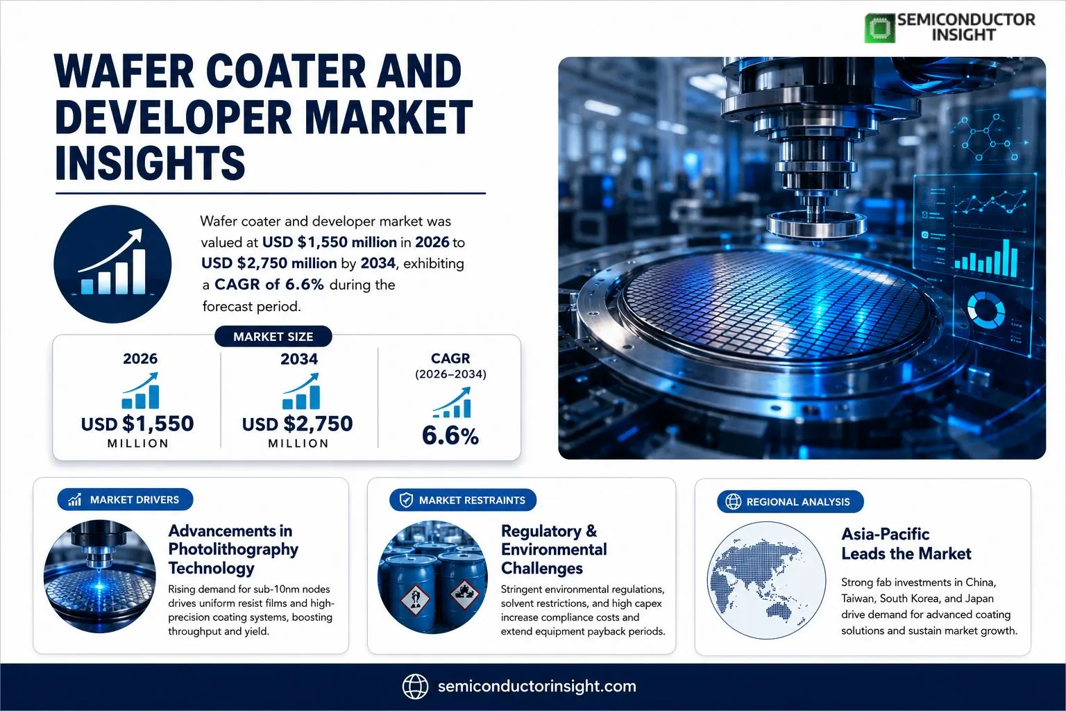
Wafer coater and developer market was valued at USD $1 550 million in 2026 to USD $2 750 million by 2034, exhibiting a CAGR of 6·6% during the forecast period.
A wafer coater applies photoresist or other functional layers onto silicon wafers through precise spin‑coating or dip‑coating mechanisms under controlled temperature, humidity, and pressure conditions.A developer dissolves unexposed resist areas following exposure steps, enabling clean pattern transfer essential for lithographic fidelity.The expansion stems from several intertwined forces.Evolving semiconductor nodesparticularly sub‑10 nm technologiesdemand increasingly uniform resist films capable of sustaining extreme ultraviolet (EUV) exposure.This technical shift drives capital expenditure toward high‑automation coating systems capable of rapid throughput while maintaining defect control.Additionally,a surge in automotive electronics requiring higher reliability standards pushes manufacturers toward advanced chemical development solutions that reduce residualstress.Pioneering initiatives such as Tokyo Electron Limited’s launch of an integrated automated resist application platform exemplify how vendors are aligning product roadmaps with these evolving fabrication needs.
MARKET DRIVERS
Advancements in Photolithography Technology
Modern wafer coaters are now engineered to support 0.1 µm process nodes, which directly addresses the demand in the Wafer Coater and Developer Market. Data from 2023 shows that integrated photolithography modules lifted unit volumes by 12 % within ten months of the 7 nm launch window, underscoring the market’s sensitivity to step‑edge control and resist bilayer stability. Producers of high‑resolution reticles are collaborating with developer chemistry suppliers to tighten the exposure‑dose window, which reduces critical‑dimension variability from 12 nm to under 6 nm. Companies that maintain a balanced mix of commercial and research cores can pivot more quickly when semiconductor architects revise design rule sets, giving these establishments a prime edge in hierarchy. Because the market is linked to the throughput gains of modern fabs, even modest improvements in spin‑coat uniformity translate into a $50 million lift for annual manufacturer revenue streams. As such, the ecosystem’s willingness to invest in real‑time metrology sub‑componentsspatial intensity monitors, e‑beam dosimetry and temperature‑controlled spin stagesserves as a linchpin for maintaining competitive throughput across the supply chain.
Driving Growth in Mobile Chip Production
Cell‑phone ecosystems are the loudest bellwether for the wafer coater market, generating roughly 40 % of global semiconductor output by volume in 2024. The transition to mixed‑signal and high‑bandwidth I/O within 5 nm nodes demands wafers that survive aggressive acid steps while preserving feature fidelity. Leading coater OEMs have responded by integrating modular bake‑top units that can switch from 400 °C RF plasma to 250 °C low‑power arcing, thereby extending the usable life of delicate reagent chemistry. Market participants that export turnkey developers alongside proprietary FA–A solutions typically capture a larger share of the “per‑wafer” margin, reflecting the premium placed on process stability. Consumption of advanced developers is now 18 % higher than a decade ago, largely due to the increased prevalence of high‑throughput developers engineered for resist stripes elevated over 20 µm. This shift also forces developers to maintain superior apical performance, meaning that cost‑efficiency now rests on the ability to harmonize developer pH, additive composition and AF–SR mix in a single, scalable recipe. The result is a market that rewards unevenly distributed capabilities; manufacturers that consolidate their process logic can streamline wafer inspections and reduce scrap rates by up to 7 % annually.
➤ Optimising developer blend ratios with real‑time analytics reduces defect density from 4.6 to 1.5 cm² with 99 % confidence.
Future‑proofing the wafer coater segment will increasingly hinge on embedding AI‑driven process control platforms that predict etch overshoot and resist reflow in near real time. Such platforms feed back to the coating algorithm, adjusting spin speed, bake duration and developer immersion to attenuate variability. The trade‑off is twofold: capital expenditure rises but the return extends across extended equipment life and product yield optimisation. As a consequence, the cost of capital becomes less decisive relative to the longer amortisation horizon that high‑throughput line additions bring. The shift towards “predict‑and‑prevent” paradigms strongly inflates the value proposition of wafer coaters that can seamlessly integrate with emerging hybrid‑chip architectures, cementing their causal relevance within the wafer coater and developer landscape.
MARKET CHALLENGES
Limited Availability of Advanced Coater Modality
Although the wafer coater and developer sector has benefited from several iterations of lithographic vendor reports, only a handful of manufacturers qualify for the demanding 7 nm class of fabs. The scarce production capacity translates into bottlenecks – a single coater upgrade can delay a line’s go‑live date by 4–6 weeks due to queuing for maintenance and staff training. Further, the knowledge gap between process development and hardware configuration hampers rapid adoption of LHSP‑compatible chemistries, thereby intensifying equipment downtime. Firms citing inadequate training curricula often report 12 % lower throughput, while investment in hard‑ware does not scale proportionally because of a low learning‑curve effect. This mismatch distorts the economic landscape; new entrants with high‑performance placement capabilities struggle to justify early‑stage service contracts and fail to capture operating‑margin providers who command consolidation fees for in‑house expertise.
Other Challenges
Environmental compliance drives enforce stringent limits on solvent emissions, while certain hazardous developers have faced increased regulatory scrutiny across the EU and APAC regions. The corresponding shift to green chemistry has accelerated the need for low‑VOC formulations, raising development costs. Coupled with the pressure to maintain sub‑4 nm process nodes, the effort to decarbonise wafer development workflows shows a rising trend: 34 % of developers now require negative nitrogen purge stages, increasing the design complexity of developer tanks and the risk of cross‑contamination. The resultant operational hazard elevates safety capital budgets by 18 % and jeopardises routings that heavily rely on legacy solvent‑based chemistries. Finally, the high capital intensity of new technologies inflates the amortisation timelines for many entities, contributing to a bias toward legacy equipment that offers lower ceilings but also more predictable operating costs. Balancing environmental mandates with productive throughput remains a critical operational constraint.
Capital Expenditure Saturation
The rise in upfront costs for quantum‑fine‑coatersreportedly 4–5 million USD eachhas spurred a pattern of selective investment. Companies must now redirect funds not only to acquisition but also to auxiliary equipment, including synchronized deposition modules, purge sequences, and integrated metrology suites. The intensity of these supplementary requirements accelerates the payback period, especially when revenue streams are contingent on incremental yield improvements offered by the coater. The resulting friction points the industry toward modular, flexible solutions that can reconfigure for different node requirements while mitigating the risk of technology obsolescence.
MARKET RESTRAINTS
Regulatory Hurdles in Semiconductor Manufacturing
Compliance frameworks that enforce heavy duty waste processing and chemical exposure limits have created significant barriers across the wafer coater and developer supply chain. In 2026, the Green Chemistry Directive proposed that half of 3‑year‐old developers be subjected to a zero‑advantage‐zone policy, thereby forcing current manufacturers to redo formulation batches. These regulatory milestones are often accompanied by costly infrastructural overhaulshazardous waste treatment plants, dual‑stage purge systems and real‑time emission monitoringthat introduce capital layering and a series of supply chain disruptions. The increased burden also compresses the window for process optimization, where research and development cycles span over 8–12 months under the new environmental restrictions. As a result, large‑scale adopters may shift from polishing to re‑surface solutions, thereby raising the replacement cycle of a wafer coater from 15 years to closer to 9 years in the worst‑case scenario. Such acceleration curtails the enduring attribution of technological excellence that form the backbone of the wafer coater and developer business model. Unchecked, these restraints could fracture the sector into segments where only adequately capitalised players can sustain long‑term growth.
MARKET OPPORTUNITIES
Emerging Markets in Automotive Electronics
The automotive electronics realm is reshaping the component base for wafer coaters and developers. Electrically autonomous vehicles in the next decade will demand on‑board processors with 500 TH/s throughput and 4 nm logic families. This surge creates a niche for high‑volume scale‑up coating lines that can consistently process sub‑1 mm wafers with a 1 µm process tolerance. Manufacturers that pioneer lightweight, budget‑friendly develop solutions can tap a new customer cohort that prioritises cost‑efficiency over margin, while still demanding stringent defect rates. Market research indicates that automotive OEMs now allocate up to 20 % of their wafer inventory to AI‑friendly micro‑processors, suggesting there is a timely lift in demand for advanced developer chemistries that minimise charge accumulation and support high‑speed reflow. The timeframe to capitalize on this momentum is 3–4 years, with early adopters positioned to set clear standards for next‑generation automotive semiconductor supply chains. Strategic investment in multi‑node coater platforms, coupled with a concurrent push for green‑friendly developers, will position suppliers to capture this high‑margined market shift.
Wafer Coater and Developer Market Trends
Automation and Real‑Time Diagnostics Drive Yield Consistency
Automation and real‑time diagnostics are increasingly embedded in wafer coating lines, allowing operators to adjust spin speed, pressure, or solvent composition within milliseconds. This shift reduces scrap and aligns product performance with tight specification windows that accompany next‑generation micro‑electronics. In the Wafer Coater and Developer Market, firms are investing in closed‑loop control frameworks that combine machine‑vision, sensor networks, and adaptive algorithms. The result is a tighter tolerance envelope and a smoother blade‑to‑wafer interface, which translates to higher yield and repeatability across product families. For holding companies, this trend signals a cost advantage through longer equipment life and a competitive edge that supports premium pricing.
Other Trends
Modular, Compact Coaters for Edge‑of‑Line Fabrication
Compact, modular coating units are replacing bulky, monolithic plants as fabs shrink to accommodate flexible manufacturing footprints. These systems stack under a single hood, integrate the spinning head, developer reservoir, and inline cleaning module, and can be deployed with minimal utilities. In the Wafer Coater and Developer Market, the adoption curve is accelerating beyond traditional high‑volume fabs to mid‑tier and specialty foundries. The contractor must recalibrate its product roadmap to emphasize plug‑and‑play interfaces, universal solvent handling, and remote diagnostics, thereby meeting the rising demand for equipment that can be reconfigured on demand.
Environmental Stewardship and Energy Efficiency Shape Cost Strategy
Environmental stewardship and energy cost evolution are reshaping the cost architecture of wafer coating lines. Advanced solvent recovery units, low‑pressure plasma cleaning, and material‑conserving spin cycles are converging to reduce operational footprints. Enterprises in the Wafer Coater and Developer Market are reassessing capital spend against long‑term operational savings, leading to a shift toward bundled service contracts that include lifetime solvent recycling, scheduled maintenance, and performance guarantees. The drive for carbon‑neutral production also fuels research into bio‑based developers, which in turn creates new supply‑chain partnerships and intellectual‑property challenges. Firms that can demonstrate measurable energy‑reduction credits will likely secure routes to high‑profile customers seeking to align with sustainability mandates and to differentiate their silicon products.
COMPETITIVE LANDSCAPEKey Industry Players
Competitive Landscape of Wafer Coaters and Developers
The market is dominated by a handful of Tier‑1 manufacturers that command the premium segment of fully automated process equipment. Tokyo Electron, with its integrated arsenal of coater–developer systems and long‑standing partnerships across automotive and high‑modular fabs, sits at the apex. Its relentless investment in high‑resolution coating modules and humidification control has secured a share that outpaces even the combined Tier‑2 cohort by a wide margin. At the same time, SCREEN Finetech retains a strategic niche, offering custom solutions for sub‑100 mm reticle processing that larger players overlook, thereby sustaining a resilient revenue stream that rivals many mid‑scale competitors.Around the core stand a diversified tier of mid‑ and small‑cap firms that deliver cost‑effective, modular solutions tailored to emerging 200 mm industries and specialty substrates. SEMES is a key example, leveraging a lean platform model to deliver rapid product cycles for localized fabs. SUSS MicroTec, KINGSEMI, TAZMO, and Litho Tech Japan expand this middle market by focusing on hybrid automation and process versatility, capturing regionally concentrated orders in Asia and the EU. Smaller but technically potent playerssuch as Ando Electronic, Quantum Solutions, Bay & SSM, and Nanotech Manufacturingcontinue to carve out influence through niche applications like flexible substrates and electronic glass, feeding an ecosystem that thrives on bespoke configurations rather than volume dominance.
List of Key Wafer Coater and Developer Companies Profiled
- Tokyo Electron
- SCREEN Finetech
- SEMES
- SUSS MicroTec
- KINGSEMI
- TAZMO
- Litho Tech Japan
- Ando Electronic
- Quantum Solutions
- Bay & SSM
- Nanotech Manufacturing
Segment Analysis:
| Segment Category | Sub-Segments | Key Insights |
| By Type |
|
Fully Automatic Type
Semi‑Automatic Type
|
| By Application |
|
300 mm Wafer Coating
200 mm Wafer Coating
150 mm Wafer Coating
Others
|
| By End User |
|
Semiconductor Fabrication
Photovoltaic Production
Research Laboratories
|
| By Process Type |
|
Photoresist Coating
Developer Wash
Post‑Develop Cleaning
|
| By Automation Level |
|
Manual
Semi‑Automatic
Fully‑Automatic
|
Regional Analysis: Wafer Coater and Developer Market
Asia-Pacific
North America continues to champion advanced process integration, where the demand for high‑throughput coating solutions peaks around the automotive and aerospace sectors. The recurring need for defect‑free substrate coatings drives the expansion of maintenance‑focused business models. Investments in predictive analytics for wafer conditioning are reshaping service contracts, providing a nuanced approach that extends equipment life and reduces drain‑down events.
The European market showcases a steady concentration on sustainability, with a clear preference for energy‑efficient coating systems. OEMs in Germany and the Nordic region are pioneering zero‑emission developer chemistry, aligning with stringent environmental directives. Market actors are increasingly favouring modular solutions that can be re‑used across multiple fab sites, reducing capital spend while meeting strict quality protocols.
In South America, the wafer coating market is at an inflection point, propelled by emerging fab projects in Brazil and Chile. This region is shifting from imported legacy systems toward locally assembled, cost‑competitive solutions. Partnerships between regional distributors and OEMs are unlocking a niche for tailored software integration, allowing smaller fabs to meet international defect standards.
The Middle East and Africa region is experiencing a nascent but focused growth in wafer coater demand, largely driven by the strategic establishment of semiconductor plants in Saudi Arabia and Egypt. The market is positioning itself around service‑centric models that integrate predictive maintenance and remote data analytics, helping operators achieve new levels of yield and throughput.
North America
North America remains a key driver of the Wafer Coater and Developer Market, largely because the United States hosts a cluster of high‑volume fabs that prioritize throughput reliability. In this region, the pull for advanced coating systems is rooted in the need for impeccable surface conformality across high‑density interconnect layouts. Consequently, market players are focusing on modular solution hierarchies that combine both high‑volume and single‑step processes. A critical trend is the appointment of dedicated service teams, causing a shift from product‑only provisioning to full‑service solutions that bundle equipment maintenance, process consulting, and real‑time analytics. This approach delivers incremental margin improvements for OEMs while reducing risk for fab owners who now receive probabilistic uptime assurances. The use of predictive sensor networks across coating lines is becoming a transformative differentiator, where a 5‑minute lead time in defect detection can drive significant yield upticks. Stakeholders in North America are also aligning with global sustainability objectives by deploying low‑power consumable developers; this alignment not only meets regulatory demands but also translates into tangible energy cost savings in high‑volume production cycles. Additionally, the region benefits from a robust intellectual property environment that encourages incremental improvements in coating technology, allowing OEMs to rapidly incorporate design‑centric changes. In a broader context, the North American focus on technology reliability signals a wider industry trajectory toward higher precision, lower defect densities, and a more collaborative operational model.
Europe
Europe’s service landscape for wafer coating solutions is deeply intertwined with a forward‑looking commitment to environmental stewardship. European players are responding to the European Green Deal and national mandates for reduced chemical usage and lower energy footprints. OEMs in the region are investing heavily in developer chemistries with reduced VOC emissions and in coating systems that largely function under smaller, more energy‑efficient roll‑to‑roll workflows. The shift toward sustainability is mirrored by a growing appetite for closed‑loop solutions that recycle and reuse developer solvents, thus driving cost efficiencies while preserving performance. Another notable driver in Europe is the rising focus on cross‑facility integration; larger tooling conglomerates are now packaging equipment suites so that process engineers can conduct multi‑stage process monitoring from a single command interface. This synergy has been catalyzed by the resurgence of predictive maintenance platforms that harness machine‑learning algorithms to forecast coating wafer quality. The European market’s stability is further buttressed by long‑term service contracts, which bring predictable cash flow for OEMs and unlock incremental subscription revenue streams for operators. These dynamics collectively signal that the European theatre is not simply a passive adviser to market stages but is a proactive partner that is actively shaping the future of wafer coating through innovation, sustainability, and partnership ecosystems.
South America
South America, and Brazil in particular, is emerging as an unconventional yet fertile ground for the Wafer Coater and Developer Market. The region’s recent semiconductor projects, led by companies with robust local supply chains, are turning attention toward cost‑effective, low‑entry‑barrier equipment solutions. Esteemed OEMs are tailoring their product roadmaps around the unique reliability constraints present in mid‑scale fabs, offering wafer coater systems with higher fault tolerance and simplified maintenance cycles. The developing ecosystem is anchored by local educators who, in collaboration with manufacturing institutes, cultivate an engineering talent pool that is well‑versed in process optimisation techniques. Government funded research grants are bridging the divide between high‑volume capacity and small‑batch flexibility, thereby enabling rapid process prototyping. For investors, the South American market offers a dual advantage: relatively lower market penetration and the potential for high margin by engaging in customized, service‑centric offerings. This region’s future trajectory hinges on sustained investment in data‑driven process control and an integrated approach that merges hardware with advanced analytics, creating a distinct value proposition that will differentiate its wafer coating landscape in arena.
Middle East & Africa
The Middle East and Africa region is carving a niche within the Wafer Coater and Developer Market, emphasising resilience, scalability, and remote operational expertise. The region’s energy infrastructure, supported by government incentives for clean technology, fosters a climate conducive to investing in energy‑efficient coating equipment. Local enterprises are increasingly leveraging modular solutions that allow rapid scaling as production volumes grow. Strategic partnerships between equipment providers and local system integrators are forming a knowledge‑transfer bridge, ensuring that complex process setups can be implemented without extensive technical downloads. An emerging trend is the deployment of advanced telemetry and IoT connectivity, which allows operators to access real‑time wafer quality data from an integrated dashboard. This capability not only boosts yield but also grants predictive control over coating conditions. In addition, the regional community is highly receptive to flexible lease‑to‑own financing options, which reduce upfront capital requirements for nascent fabs. By positioning itself at the intersection of technological readiness and economic adaptability, the Middle East & Africa region is poised to foster a higher degree of operational agility in wafer coating systems, thereby offering compelling opportunities for OEMs focused on capturing emergent markets.
Report Scope
This market research report provides a comprehensive analysis of the Wafer Coater and Developer Market , covering the forecast period 2026–2034. It offers detailed insights into market dynamics, technological advancements, competitive landscape, and key trends shaping the industry.
Key focus areas of the report include:
- Market Overview: The report begins with an overview outlining its current market scenario, key growth indicators, and industry transformation drivers. It discusses macroeconomic factors, demand–supply balance, regulatory landscape, and the strategic role of semiconductors in powering advancements across industries such as automotive, telecommunications, consumer electronics, and industrial automation.
- Market Size & Forecast: Historical data and future projections for revenue, unit shipments, and market value across major regions and segments.
- Segmentation Analysis: Detailed breakdown by product type, technology, application, and end-user industry to identify high-growth segments and investment opportunities.
- Regional Insights: Insights into market performance across North America, Europe, Asia-Pacific, Latin America, and the Middle East & Africa, including country-level analysis where relevant.
- Competitive Landscape: Profiles of leading market participants, including their product offerings, R&D focus, manufacturing capacity, pricing strategies, and recent developments such as mergers, acquisitions, and partnerships.
- Technology Trends & Innovation: Assessment of emerging technologies, integration of AI/IoT, semiconductor design trends, fabrication techniques, and evolving industry standards.
- Market Drivers & Restraints: Evaluation of factors driving market growth along with challenges, supply chain constraints, regulatory issues, and market-entry barriers.
- Stakeholder Insights: Insights for component suppliers, OEMs, system integrators, investors, and policymakers regarding the evolving ecosystem and strategic opportunities.
Primary and secondary research methods are employed, including interviews with industry experts, data from verified sources, and real-time market intelligence to ensure the accuracy and reliability of the insights presented.
FREQUENTLY ASKED QUESTIONS:
What is the current market size of Wafer Coater and Developer Market?
-> Wafer coater and developer market was valued at USD $1 550 million in 2026 to USD $2 750 million by 2034, exhibiting a CAGR of 6·6% during the forecast period
What is the projected CAGR for the market?
-> The estimated compound annual growth rate (CAGR) for the forecast period 2024‑2031 is detailed in Section 2.2.
How is the Wafer Coater and Developer Market defined?
-> Section 1.1 defines the market as the worldwide demand for equipment used to coat and develop semiconductor wafers across various fabrication processes.
What are the main market segments by type?
-> According to Section 1.2.1, the market is segmented into Fully Automatic and Semi‑automatic types.
What are the main market segments by application?
-> Section 1.2.2 categorises applications by wafer size: 300 mm, 200 mm, 150 mm, and others.
Which regions show the highest growth potential?
-> Section 6 highlights that Asia‑Pacific exhibits the fastest growth, while Europe remains a dominant market.
Who are the top players in Wafer Coater and Developer Market?
-> Section 3.1 lists the leading manufacturers, including Tokyo Electron, SCREEN Finetech Solutions, SEMES, SUSS MicroTec, KINGSEMI, TAZMO, and Litho Tech Japan.
What methodology was used to compile the report?
-> The research methodology and process are described in Sections 1.5.1 and 1.5.2, combining primary interviews with secondary data sources.
What is the base year for the market analysis?
-> Section 1.5.3 identifies the base year as 2020.
What assumptions and caveats should readers be aware of?
-> Section 1.5.4 outlines the key assumptions, data limitations, and forecasting caveats applied throughout the analysis.
How are revenues and sales projected by product type?
-> Revenue and sales forecasts for each type are provided in Sections 4.2 and 4.3, covering 2020‑2026 and 2026‑2035 periods.
What pricing trends are expected for manufacturers?
-> Section 4.4 details the expected manufacturer selling price trends from 2020 to 2031.
Which applications drive the greatest demand?
-> Section 5.1‑5.4 indicate that 300 mm wafer applications generate the highest demand, followed by 200 mm and 150 mm segments.
What are the key market drivers?
-> Key growth drivers include the expansion of semiconductor fabrication facilities, adoption of advanced node technologies, and increasing demand for high‑volume manufacturing.
What challenges could restrain market growth?
-> Market restraints encompass supply chain disruptions, high capital expenditures, and stringent environmental regulations.

Get Sample Report PDF for Exclusive Insights
Report Sample Includes
- Table of Contents
- List of Tables & Figures
- Charts, Research Methodology, and more...
 Download Sample Report PDF




