
Key Statistics
Key Takeaways
- Lithography is the largest individual equipment category because leading-edge logic and memory require the most capital-intensive patterning tools and increasingly complex exposure strategies. EUV and High-NA EUV concentrate value at the top end, while mature-node fabs continue purchasing DUV systems, coaters/developers and complementary patterning equipment.
- Foundry and logic is the largest application segment, supported by AI accelerators, high-performance computing and the transition toward gate-all-around architectures at 2 nm and below. SEMI projected foundry-and-logic wafer-fab-equipment sales at USD 78.0 billion in 2026, illustrating how strongly advanced logic is shaping front-end capital allocation.
- Asia Pacific accounts for more than 60% of demand because Taiwan, South Korea, China and Japan host the world’s largest concentration of foundry, memory and semiconductor manufacturing capacity. China, Taiwan and Korea have repeatedly ranked among the largest equipment-spending destinations, while Japan remains strategically important in equipment, materials and mature-node production.
- AI is raising process intensity, not only fab capacity. HBM, advanced DRAM, gate-all-around logic and 3D NAND require more deposition, etch, cleaning, metrology and inspection steps per wafer. This creates equipment growth even when wafer-start growth is more modest, because each new device generation needs additional process control and tighter tolerances.
- High-NA EUV, conductor etch, selective deposition and sub-nanometer metrology are becoming core technology inflections. ASML, Lam Research and Applied Materials introduced or advanced systems in 2025–2026 aimed at 2 nm logic, advanced memory and AI-oriented devices, increasing both tool ASP and customer dependence on a small group of highly specialized suppliers.
- Capacity constraints sit in precision supply chains and qualification rather than simple factory floor space. Front-end tools contain specialized optics, vacuum systems, RF power, motion control, lasers, ceramics and metrology subsystems. Long component lead times and strict customer qualification make supplier-network resilience a strategic part of equipment availability.
Semiconductor Front-End Equipment Market Overview
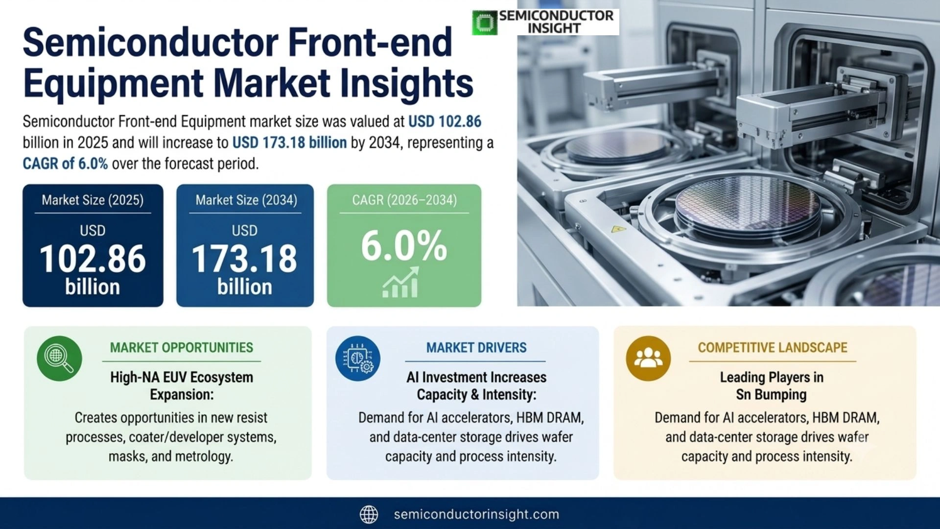
Semiconductor Front-end Equipment Market was valued at approximately USD 102.86 billion in 2025 and is projected to reach approximately USD 173.18 billion by 2034, representing a 6.0% CAGR during 2026–2034. Asia Pacific accounts for more than 60% of demand, reflecting the concentration of foundry, logic, DRAM and NAND manufacturing in Taiwan, South Korea, China and Japan.
Semiconductor front-end equipment comprises the production systems used before wafer dicing and final assembly to create devices on the silicon wafer. The market includes etch systems, lithography machines, metrology and inspection, deposition systems, cleaning equipment, CMP equipment and other wafer-fabrication tools. These systems perform repeated cycles of film formation, pattern definition, material removal, cleaning and measurement, and their performance determines device geometry, yield, throughput and cost.
Front-end equipment demand is driven by two overlapping forces: capacity expansion and process complexity. A new fab requires a complete tool set, but a technology migration inside an existing fab can also create substantial demand because newer devices require more layers, tighter process windows and additional inspection. Gate-all-around logic, HBM-related DRAM and very high-layer-count 3D NAND increase deposition, etch and metrology intensity even when the number of wafers processed does not increase proportionally.
SEMI’s broader wafer-fab-equipment benchmark illustrates the scale of this investment cycle. The association reported record WFE sales of USD 116.9 billion in 2025 and forecast USD 143.9 billion for 2026, driven by advanced memory and leading-edge logic. The report market is not identical to SEMI’s WFE definition, but the industry benchmark confirms the direction of capital spending and the increasing share of investment tied to AI, HBM and 2 nm-class production.
Technology concentration makes this market structurally different from most industrial machinery sectors. EUV lithography depends on ASML’s unique systems and an extensive optical supply network; conductor etch and deposition platforms rely on highly proprietary plasma and materials science; inspection requires advanced optics, e-beam and computational algorithms. Customers therefore qualify tools over long periods and rarely switch suppliers casually, which supports strong pricing and long service relationships for established equipment platforms.
Segment Analysis: By Type
By type, the market is segmented into Semiconductor Etch Equipment, Lithography Machines, Semiconductor Metrology and Inspection, Semiconductor Deposition System, Semiconductor Cleaning Equipment, CMP Equipment and Others. Lithography represents the largest value category because EUV and advanced DUV systems carry exceptionally high selling prices, while etch and deposition capture strong incremental growth as device structures become more three-dimensional.
| Type | Process role | Market position |
|---|---|---|
| Semiconductor Etch Equipment | Plasma and chemical etch systems selectively remove dielectric, metal and semiconductor materials after patterning. Advanced devices need anisotropic profiles, high selectivity and precise control through deep or extremely narrow structures. Conductor etch is critical for gate, interconnect and memory patterning, while dielectric etch enables contacts and high-aspect-ratio holes. | One of the largest and fastest-growing categories. 3D NAND layer growth, HBM, GAA structures and advanced logic increase etch-step count and process difficulty. Lam Research’s Akara platform, introduced in 2025, targets atomic-scale conductor etch with plasma response 100 times faster than previous control architectures. |
| Lithography Machines | Lithography equipment transfers circuit patterns onto photoresist using DUV or EUV light, supported by mask, track and computational-control systems. Leading-edge logic and advanced DRAM increasingly depend on EUV, while High-NA EUV extends single-exposure resolution for future nodes and can reduce multi-patterning complexity. | Largest value segment. High system ASPs and ASML’s EUV technology leadership concentrate value at the top end. In 2026, ASML reported High-NA EUV production readiness milestones at Intel, showing the technology moving from R&D qualification toward real manufacturing use. |
| Semiconductor Metrology and Inspection | Optical, e-beam and hybrid systems identify particles, pattern defects, overlay errors, line-edge variation and process drift. As features shrink and structures become three-dimensional, a smaller defect can destroy more device value, increasing the economic importance of detecting excursions quickly and feeding data back into process control. | A high-value, process-control-intensive segment. AI and 3D device architectures create more difficult inspection targets, while sub-nanometer process windows increase demand for e-beam and computational metrology. Applied Materials’ PROVision 10, introduced in 2025, targets sub-nanometer resolution and deep imaging for complex 3D devices. |
| Semiconductor Deposition System | CVD, PVD, ALD, epitaxy and other deposition tools create insulating, conductive and semiconducting films with nanometer or atomic-scale control. GAA transistors, HBM and 3D NAND require conformal coatings and increasingly selective material placement across complex surfaces. | Strong structural growth segment. New materials and 3D architectures increase deposition steps even when wafer volume is stable. Selective deposition, atomic-layer processes and advanced epitaxy can eliminate downstream patterning steps or enable device structures that conventional blanket deposition cannot form economically. |
| Semiconductor Cleaning Equipment | Wet and dry cleaning tools remove particles, organic residue, metals and process by-products between fabrication steps. As features shrink, contamination that once had little effect can bridge or deform critical structures, making damage-free cleaning and selective residue removal central to yield. | A steady-to-growing segment whose value rises with process-step count. Advanced nodes and 3D structures require more cleans, more selective chemistries and tighter particle control. Suppliers differentiate through single-wafer productivity, batch cost efficiency and the ability to remove residues without collapsing fragile patterns. |
| CMP Equipment | Chemical mechanical planarization systems flatten dielectric and metal layers using slurry chemistry and controlled polishing. Planarity is essential before lithography and bonding, and the process is repeated across interconnect stacks, memory structures and some advanced packaging flows. | A smaller but strategically important category. More metal layers, hybrid bonding and advanced memory increase planarization requirements. Equipment demand is linked to process control, endpoint detection, defect reduction and integration with slurry and pad ecosystems. |
| Others | Includes thermal processing, ion implantation, track systems, wafer handling and specialized front-end tools that do not fit the major categories above. These systems remain essential because device fabrication requires dopant introduction, annealing, resist processing and numerous support processes around the core patterning cycle. | A diversified segment. Growth varies by technology transition: ion implant intensity changes with device architecture, thermal equipment benefits from new materials, and resist-track systems gain from EUV adoption and more stringent defect control. |
Technology node as a secondary segmentation
The report also segments demand by technology node into >28 nm, 20–28 nm, 10–20 nm and <10 nm. Mature nodes remain commercially important because analog, power, display driver, automotive and industrial devices continue to expand on 28 nm and older processes. However, equipment revenue per wafer is highest below 10 nm because EUV, tighter metrology, more complex etch and advanced deposition dramatically increase tool intensity and ASP.
Segment Analysis: By Application
By application, the market is segmented into Foundry and Logic Equipment, NAND Equipment, DRAM Equipment and Others. Foundry and logic is the largest application because leading-edge AI and HPC accelerators are pushing foundries toward 2 nm gate-all-around production. DRAM is the fastest-changing memory application because HBM increases wafer-fab equipment intensity, while NAND remains highly sensitive to layer-count migration and capacity cycles.
| Application | Demand characteristics |
|---|---|
| Foundry and Logic Equipment | Largest application. Leading-edge foundries and IDMs require EUV lithography, advanced conductor and dielectric etch, atomic-scale deposition, selective process control and high-sensitivity inspection for 5 nm, 3 nm and 2 nm-class nodes. SEMI forecast foundry-and-logic WFE sales at USD 78.0 billion in 2026 as AI accelerators and high-performance computing drive advanced-node capacity expansion. |
| NAND Equipment | 3D NAND growth is driven by more memory layers and denser vertical structures rather than simple planar shrink. Each layer increase can add deposition, high-aspect-ratio etch and cleaning requirements. SEMI forecast NAND-related WFE sales at USD 13.9 billion in 2026, up 30.7% year over year, as manufacturers invest in higher-density architectures. |
| DRAM Equipment | Fastest memory investment cycle. HBM demand and advanced DRAM node migration are increasing equipment spending on lithography, deposition, etch and process control. SEMI projected DRAM WFE sales at USD 38.8 billion in 2026, 39% above 2025, indicating a major shift in capital allocation toward AI-oriented memory. |
| Others | Other demand includes analog, power, image sensors, specialty logic and compound-semiconductor processes. These applications use a wider range of mature nodes and wafer sizes, creating demand for cost-efficient new and refurbished equipment. Growth is steadier than advanced logic but strategically important because automotive, industrial and energy systems depend heavily on specialty semiconductor capacity. |
Regional Analysis
Asia Pacific dominates front-end equipment demand with more than 60% share because the region hosts the largest concentration of advanced foundry, memory and mature-node fabs. North America is expanding through CHIPS-related manufacturing and AI logic investment, Europe combines ASML’s equipment leadership with automotive and power-semiconductor fabs, while the Middle East and South America remain much smaller front-end equipment markets.
How does regional demand differ across the semiconductor front-end equipment market?
Regional equipment demand follows actual wafer-fab construction and technology migration rather than end-device consumption. Taiwan and South Korea buy advanced logic and memory tools, China combines very large mature-node and localization investment, Japan supports both equipment manufacturing and specialty fabs, and the United States is adding leading-edge capacity through major foundry and IDM projects. Europe has lower total wafer capacity but exceptional strategic importance because ASML and ASM anchor critical process technologies.
| Region | Position | Growth outlook | Demand profile | What decides supplier selection |
|---|---|---|---|---|
| Asia Pacific | Largest – >60% | High | Foundry, memory and mature-node capacity led | Process performance, installed-base support, local service, export compliance and high-volume manufacturing readiness |
| North America | Second-tier demand / top innovation base | High | AI logic, domestic fab expansion and equipment R&D led | Leading-edge capability, service depth, trusted supply and domestic manufacturing support |
| Europe | Strategic equipment technology region | Moderate to high | Lithography leadership, automotive, power and specialty semiconductors | Technology differentiation, energy efficiency, regulatory compliance and proximity to European fabs |
| Middle East & Africa | Emerging | Low to moderate from small base | Israel specialty fabs and early regional investment led | Local ecosystem depth, service support, project bankability and technology-transfer constraints |
| South America | Nascent | Low to moderate from small base | Mature-node, R&D and back-end-adjacent activity led | Capital availability, refurbished tool economics, technical support and imported spare parts |
Key Semiconductor Front-End Equipment Manufacturers and Competitive Landscape
Competition is highly concentrated by process step because each category depends on years of proprietary engineering, customer qualification and installed-base support. Lithography is the most concentrated because EUV has only one production supplier. Etch, deposition and cleaning have broader competition but still depend on differentiated plasma, chemistry and chamber designs. Inspection and metrology are similarly concentrated because optical and e-beam systems require both precision hardware and sophisticated computational algorithms.
Customer switching costs are high. A tool is qualified not only for basic functionality but for process recipe, defectivity, throughput, chamber matching, maintenance intervals and integration with factory automation. Replacing an incumbent platform can require months of process development and yield validation. This creates durable installed bases and makes service capability, spare-parts availability and field-engineering responsiveness critical competitive assets.
The competitive landscape is also becoming more solution-oriented. Equipment companies increasingly connect several process steps through shared data, chamber integration and advanced process control. AI and 3D devices amplify this trend because a change in deposition can affect etch, metrology and yield downstream. Suppliers with broad portfolios can therefore use cross-process learning to improve customer outcomes, while specialists defend positions through unmatched performance in one critical step.
Key Industry Players
- ASML Holding N.V.
- Applied Materials, Inc.
- Tokyo Electron Limited (TEL)
- Lam Research Corporation
- KLA Corporation
- ASM International
- Ebara Corporation
- NAURA Technology Group
- SEMES
- Hitachi High-Tech
- Canon Inc.
- Nikon Corporation
- Onto Innovation
- Camtek Ltd.
- Veeco Instruments
Semiconductor Front-End Equipment Production Capacity Analysis
Front-end equipment capacity depends on precision manufacturing, specialized subsystem supply and customer-installation capability. A major tool may contain vacuum chambers, high-purity gas systems, RF generators, high-accuracy stages, optics, lasers, ceramics, sensors and complex software sourced from a global network. ASML reported more than 5,100 suppliers in 2025, illustrating the scale of the supply base required for advanced lithography alone. Effective capacity therefore depends on synchronized component availability rather than final assembly space.
Capacity expansion is occurring in both Asia and the United States. Tokyo Electron completed a JPY 52 billion development building in Miyagi in 2025 and separately announced a planned JPY 104 billion production building for semiconductor equipment including plasma etch systems, with completion targeted for 2027. Applied Materials, Lam Research and other suppliers are also investing in R&D and manufacturing ecosystems to support AI-driven equipment demand and increasingly complex customer roadmaps.
Service capacity is equally important because tools are installed and maintained inside customer fabs under strict uptime requirements. EUV systems, plasma etchers and high-end inspection tools require specialized field engineers, spare parts and software support. A vendor can therefore face a commercial capacity constraint even when it can manufacture another tool if it lacks trained personnel to install, qualify and support additional systems across multiple geographic regions.
Technology transitions can abruptly change the required capacity mix. High-NA EUV increases demand for new lithography platforms and track systems; HBM increases advanced DRAM equipment; 3D NAND increases high-aspect-ratio etch and deposition; GAA logic increases selective deposition and metrology. Suppliers must therefore invest ahead of customer adoption, carrying R&D and factory risk years before a process becomes high-volume manufacturing.
Semiconductor Front-End Equipment Market Dynamics
The market grows through a combination of new fab capacity, technology migration and rising process complexity. AI, HBM and 2 nm-class logic are raising equipment intensity per wafer, while national semiconductor policies diversify manufacturing geographically. Growth is restrained by extreme tool cost, long development cycles, export controls and supply-chain concentration. The strongest opportunities are High-NA EUV, atomic-scale etch and deposition, AI-enabled process control, advanced memory and lower-emission manufacturing platforms.
MARKET DRIVERS
Drivers Impact Analysis*
| Market Factor | Directional Impact on CAGR Forecast* | Commercial Mechanism |
|---|---|---|
| AI-driven leading-edge logic and HBM investment | +1.6 to +2.3 percentage points | AI accelerators and high-bandwidth memory require advanced-node capacity and more process steps, increasing lithography, etch, deposition and inspection intensity. |
| Technology migration to GAA, High-NA and 3D structures | +1.1 to +1.7 percentage points | New architectures demand new tools or major upgrades even when total wafer starts are stable, supporting recurring capital spending. |
| Regional fab localization and incentives | +0.7 to +1.1 percentage points | U.S., European, Japanese and other policies create additional equipment demand as capacity is diversified geographically. |
AI investment increases both wafer capacity and process intensity
AI accelerators require leading-edge logic, while HBM increases advanced DRAM investment and data-center storage supports NAND. SEMI forecast WFE sales of USD 143.9 billion in 2026, including USD 78.0 billion for foundry and logic and USD 38.8 billion for DRAM. The commercial importance is that AI drives multiple equipment categories simultaneously, from EUV and etch to deposition, clean and metrology, rather than benefiting only one tool segment.
Gate-all-around and three-dimensional devices add more difficult process steps
Planar scaling has increasingly been replaced by complex 3D device structures. GAA transistors require conformal deposition, selective material removal and more demanding metrology around nanosheet structures. 3D NAND requires deep high-aspect-ratio etch and repeated deposition across hundreds of layers. Each architecture adds opportunities for specialized equipment and increases the value of process control because a defect in one difficult step can destroy substantial downstream wafer value.
High-NA EUV extends lithography capital intensity
ASML’s High-NA platform raises numerical aperture from 0.33 to 0.55 and is designed to print substantially smaller features in a single exposure. The EXE:5200B targets 8 nm resolution and higher imaging contrast, reducing some multi-patterning while creating a new generation of high-value tools, masks, tracks and process-control requirements. Intel’s 2026 production milestone demonstrates that High-NA is progressing from qualification toward manufacturing use.
Government-supported fab localization multiplies regional tool demand
A wafer fab requires a full front-end tool set regardless of whether the global industry already has sufficient capacity elsewhere. U.S., European and Japanese incentives therefore create incremental equipment demand when companies build geographically diversified fabs. Localization also increases service and spare-parts requirements because equipment suppliers must support installations in new clusters rather than concentrating field resources only in established Asian manufacturing hubs.
MARKET RESTRAINTS
Restraints Impact Analysis*
| Market Factor | Directional Impact on CAGR Forecast* | Commercial Mechanism |
|---|---|---|
| Extreme capital cost and long customer cycles | −0.9 to −1.4 percentage points | Advanced tools can cost tens or hundreds of millions of dollars and require long qualification, concentrating purchases among large chipmakers. |
| Export controls and geopolitical restrictions | −0.7 to −1.1 percentage points | Technology restrictions can limit shipment of advanced lithography, etch and deposition systems to major markets and reshape supplier strategy. |
| Specialized supply-chain bottlenecks | −0.5 to −0.9 percentage points | Optics, RF power, ceramics, precision motion and other custom subsystems can constrain tool output despite strong end-market demand. |
Tool economics limit the customer base
A leading-edge fab can require tens of billions of dollars in total capital, and individual EUV systems have extremely high purchase prices. Equipment suppliers therefore depend on a relatively small number of customers capable of funding advanced nodes. Downturns in memory or consumer electronics can cause sudden order changes because customers defer capital rather than continue spending evenly through the cycle. This cyclicality remains a structural feature even in a strong long-term growth market.
Export controls distort market access and product roadmaps
Advanced semiconductor equipment has strategic importance, and the United States, Netherlands, Japan and other jurisdictions maintain restrictions affecting shipments to certain Chinese fabs and technology nodes. Vendors must manage licensing, product classification and customer-specific rules. Restrictions can reduce reachable demand for the most advanced platforms while simultaneously encouraging domestic Chinese investment in local etch, deposition, cleaning and lithography equipment.
Precision subsystem concentration can slow deliveries
Advanced tools require specialized components that are not easily substituted. High-end optics, laser sources, vacuum valves, electrostatic chucks, ceramics and motion systems may be qualified from only a handful of suppliers. A shortage can therefore hold up delivery of a complete tool even when most of the bill of materials is available. Equipment companies increasingly dual-source where possible, but many critical components remain technologically concentrated.
MARKET OPPORTUNITIES
High-NA EUV ecosystem expansion
High-NA EUV creates opportunities beyond the scanner itself. Customers need new resist processes, coater/developer systems, masks, metrology and inspection capable of handling tighter imaging requirements. As High-NA moves toward broader insertion in 2027–2028, suppliers around the lithography ecosystem can capture new spending even if they do not manufacture exposure tools.
Atomic-scale etch and selective deposition
GAA transistors, advanced DRAM and high-layer-count NAND increasingly require material removal and deposition with near-atomic selectivity. Lam’s Akara conductor etch and Applied Materials’ Xtera epitaxy system show how equipment vendors are creating new platforms around these difficult process windows. Suppliers that solve a specific scaling bottleneck can gain share rapidly because customers have few alternatives once a process reaches high-volume production.
AI-enabled metrology and process control
Three-dimensional devices generate more inspection data and more complex defect signatures. Process-control suppliers can use machine learning, computational imaging and e-beam data fusion to identify excursions faster and recommend recipe changes. The commercial opportunity extends beyond equipment ASP into software and recurring analytics because fabs need continuous yield optimization across a rapidly growing installed base.
Energy-efficient and lower-emission fab equipment
Semiconductor fabs consume substantial electricity, water and process gases. Customers increasingly evaluate tool energy use, abatement requirements, chemical consumption and cleanroom footprint alongside throughput. Equipment vendors that reduce chamber emissions, shorten process time or increase wafer throughput per square meter can create measurable operating-cost savings, supporting upgrades even when the underlying process node does not change.
Semiconductor Front-End Equipment Supply Chain Analysis
The front-end equipment supply chain spans precision subsystems and materials, tool manufacturing and integration, customer fab installation, and recurring service and upgrades. Value capture is unusually concentrated at the tool and lifecycle-service stages because proprietary process chambers, optics, software and recipes determine customer yield. However, upstream subsystem suppliers can become critical bottlenecks when their component cannot be replaced without redesigning or requalifying the equipment platform.
Stage 1 – Specialized subsystem suppliers
Upstream suppliers provide components whose performance can determine the entire tool. EUV optics require extraordinary surface precision; plasma tools depend on stable RF and vacuum systems; inspection systems rely on high-speed cameras, e-beam sources and motion stages. Because many components are custom-designed, equipment OEMs collaborate closely with suppliers and may carry strategic inventory or capacity agreements to protect production schedules.
Stage 2 – Equipment OEM integration
Equipment manufacturers convert subsystems into a repeatable production platform through chamber design, process physics, controls and software. This is where most intellectual property and differentiation sit. The same vacuum chamber can produce very different customer value depending on plasma uniformity, defectivity, recipe stability and throughput. Large OEMs also run extensive internal process labs to demonstrate customer wafers before a tool is purchased.
Stage 3 – Customer installation and process qualification
A front-end tool is not commercially useful when it leaves the factory; it must be installed, connected to ultra-pure utilities, calibrated and qualified in the customer’s process flow. Installation can take weeks or months for complex systems. Field engineers and application specialists therefore form a capacity layer of their own, and a vendor’s ability to support simultaneous fab ramps can influence whether a customer awards additional tool positions.
Stage 4 – Installed-base services and upgrades
Advanced tools operate for many years and receive maintenance, chamber replacements, software updates and productivity upgrades throughout their life. ASML, Applied Materials, Lam and other suppliers generate substantial recurring revenue from installed-base support. Upgrades can be economically attractive to customers because increasing throughput or reducing defectivity on an existing qualified platform may deliver capacity faster than installing a completely new tool.
Recent Developments in the Semiconductor Front-End Equipment Market
ASML announced that Intel Foundry had entered high-volume manufacturing for a subset of Intel Core Ultra Series 3 processors using High-NA EUV on specific Intel 18A layers. The milestone moves High-NA from R&D qualification toward production use and strengthens the case for a new investment cycle in scanners, tracks, metrology, masks and process-development infrastructure.
SEMI forecast 2026 WFE sales at USD 143.9 billion, up 23.1% year over year, driven by advanced memory and leading-edge logic. The association projected foundry/logic WFE at USD 78.0 billion and DRAM WFE at USD 38.8 billion, confirming that AI accelerators, HBM and 2 nm-class production are increasing front-end equipment spending across multiple process categories.
Tokyo Electron released the CLEAN TRACK LITHIUS Pro DICE 300 mm coater/developer. TEL said the platform can cut coating-related wafer defects by 50% or more and improve productivity and environmental performance by at least 25% compared with prior models. The system is designed to support advanced EUV and High-NA patterning, where resist uniformity and defect control are increasingly critical.
Applied Materials launched Kinex, Xtera and PROVision 10 systems targeting die-to-wafer hybrid bonding, advanced gate-all-around epitaxy and high-resolution e-beam metrology. The launch demonstrates how front-end equipment vendors are broadening around AI-related device complexity, with new tools designed to improve transistor performance, memory integration and process control at 2 nm and beyond.
Lam Research introduced Akara, a conductor etch system designed for atomic-scale precision in advanced 3D chipmaking. Lam said its DirectDrive plasma technology can respond 100 times faster than previous control approaches, giving customers tighter control of critical etch profiles. The product targets scaling challenges in advanced logic and memory where process variability can materially affect yield.
REPORT SCOPE & SEGMENTATION
| Study Period | 2020–2034 |
| Base Year | 2025 |
| Estimated Year | 2026 |
| Forecast Period | 2026–2034 |
| Historical Period | 2020–2025 |
| Market Size 2025 | USD 102.86 Billion |
| Market Size 2034 | USD 173.18 Billion |
| Growth Rate | CAGR of 6.0% from 2026–2034 |
| Largest Market 2025 | Asia Pacific – more than 60% |
| Unit | Value (USD Billion) and equipment sales |
| Segmentation | By Type, By Application, By Technology Node, By End User and By Region |
| By Type | Semiconductor Etch Equipment · Lithography Machines · Semiconductor Metrology and Inspection · Semiconductor Deposition System · Semiconductor Cleaning Equipment · CMP Equipment · Others |
| By Application | Foundry and Logic Equipment · NAND Equipment · DRAM Equipment · Others |
| By Technology Node | >28 nm · 20–28 nm · 10–20 nm · <10 nm |
| By End User | Integrated Device Manufacturers (IDMs) · Foundries · Memory Manufacturers · Others |
| By Region | North America · Europe · Asia Pacific · South America · Middle East & Africa |
| Companies Profiled | ASML Holding N.V. · Applied Materials, Inc. · Tokyo Electron Limited · Lam Research Corporation · KLA Corporation · ASM International · Ebara Corporation · NAURA Technology Group · SEMES · Hitachi High-Tech · Canon Inc. · Nikon Corporation · Onto Innovation · Camtek Ltd. · Veeco Instruments |
| Customization Scope | Country, regional, device, node, equipment category, fab project and company-level customization can be added to align the study with customer-specific capacity and procurement requirements. |
Frequently Asked Questions
What is the size of the semiconductor front-end equipment market in 2025?
The global semiconductor front-end equipment market was valued at approximately USD 102.86 billion in 2025. The scope includes etch, lithography, metrology and inspection, deposition, cleaning, CMP and other equipment used to fabricate semiconductor devices on wafers before final assembly and packaging.
What is the projected market size by 2034?
The market is projected to reach approximately USD 173.18 billion by 2034, representing a 6.0% CAGR during 2026–2034. Growth is driven by AI-related leading-edge logic, HBM, 3D NAND, regional fab construction and process-intensity increases from advanced device architectures.
Which region leads the market?
Asia Pacific accounts for more than 60% of front-end equipment demand because Taiwan, South Korea, China and Japan host the world’s largest concentration of foundry, memory and mature-node semiconductor manufacturing. The region also has dense equipment, materials and service ecosystems.
Which equipment type is the largest?
Lithography machines represent the largest individual value category because EUV and advanced DUV systems carry very high selling prices and are critical to leading-edge patterning. Etch and deposition also represent major growth categories because 3D NAND, GAA and advanced memory increase process-step complexity.
Which application is the largest?
Foundry and logic equipment is the largest application. AI accelerators, high-performance computing and premium mobile processors are driving foundries toward 3 nm and 2 nm-class production, increasing demand for EUV lithography, conductor and dielectric etch, deposition and high-sensitivity process control.
How is AI changing front-end equipment demand?
AI affects several device categories at once. Accelerators increase advanced logic investment, HBM raises DRAM equipment intensity and data-center storage supports NAND. More importantly, these devices use complex 3D structures and tighter process windows, increasing the number and technical difficulty of etch, deposition, cleaning and inspection steps per wafer.
Why is High-NA EUV important?
High-NA EUV increases numerical aperture from 0.33 to 0.55, enabling smaller single-exposure features and higher transistor density. ASML’s EXE:5200B targets 8 nm resolution, and Intel demonstrated production readiness in 2026. The transition creates demand not only for scanners but also tracks, masks, metrology and supporting process development.
What are the main market restraints?
The main restraints are extreme capital cost, long equipment-development and qualification cycles, export controls, semiconductor spending cyclicality and concentration in specialized subsystems. A shortage of optics, RF generators, ceramics or precision motion components can delay a tool even when most other parts are available.
Which companies are profiled in the report?
The report profiles ASML, Applied Materials, Tokyo Electron, Lam Research, KLA, ASM International, Ebara, NAURA, SEMES, Hitachi High-Tech, Canon, Nikon, Onto Innovation, Camtek and Veeco Instruments. The competitive landscape varies sharply by process step, with different leaders in lithography, etch, deposition, cleaning and inspection.
What is the strongest long-term opportunity?
The strongest opportunities are High-NA EUV, atomic-scale etch and deposition, AI-enabled process control, HBM-related DRAM equipment, 2 nm gate-all-around production, higher-layer 3D NAND and lower-emission fab technologies. These trends increase equipment value per wafer and support recurring upgrades throughout the installed tool base.

Get Sample Report PDF for Exclusive Insights
Report Sample Includes
- Table of Contents
- List of Tables & Figures
- Charts, Research Methodology, and more...
 Download Sample Report PDF





