Wafer Fabrication Equipment Market Insights
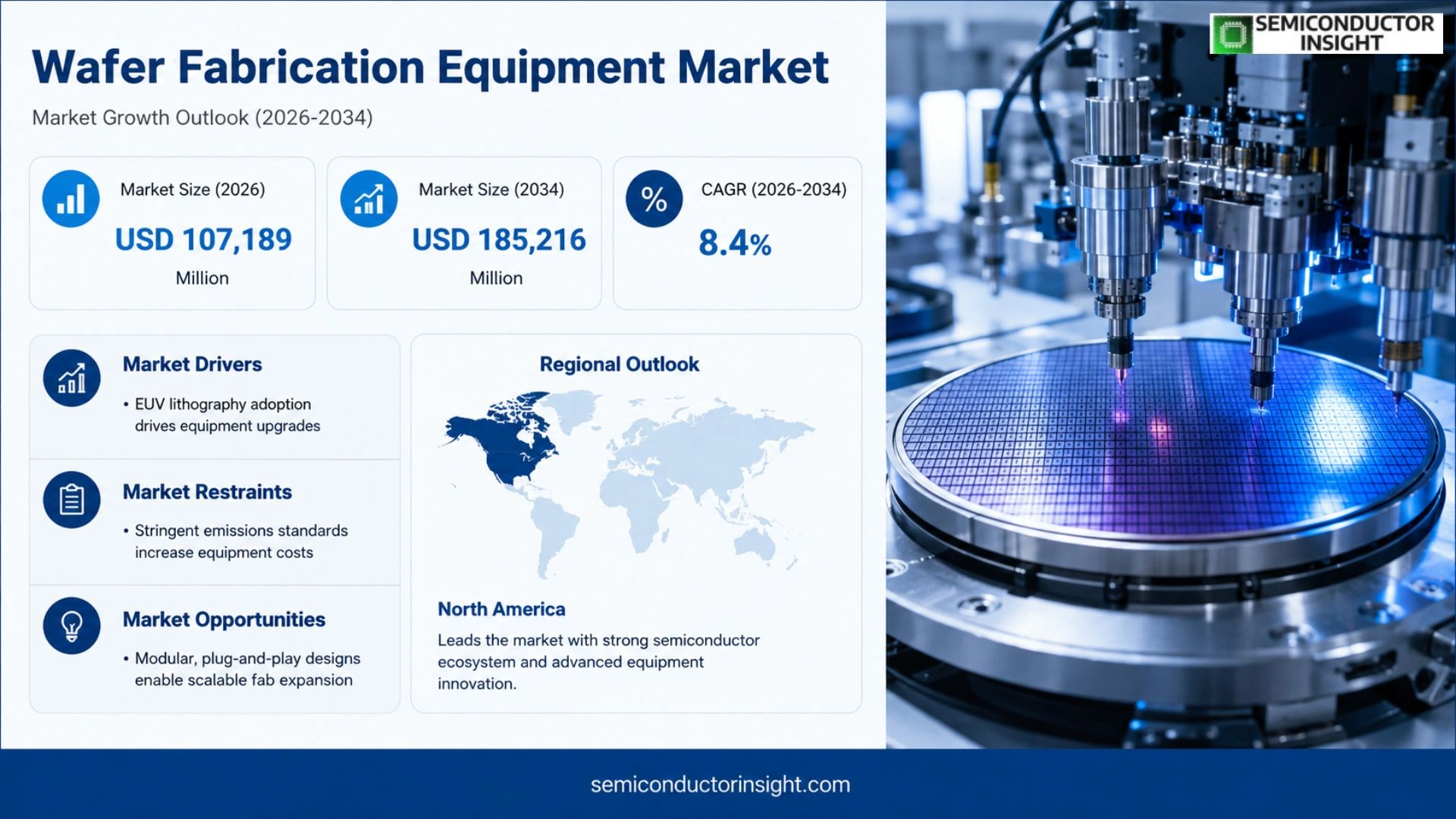
Global Wafer Fabrication Equipment market is projected to grow from USD 107,189 million in 2026 to USD 185,216 million by 2034, exhibiting a CAGR of 8.4% during the forecast period.
Wafer Fabrication Equipment refers to the core semiconductor equipment used in wafer processing, covering the entire manufacturing chain from bare wafers to fully processed integrated circuits. Major product categories include lithography systems, etching equipment, deposition equipment (CVD, PVD, ALD), ion implanters, oxidation/diffusion furnaces, chemical‑mechanical polishing (CMP) equipment, wafer cleaning systems and metrology/inspection tools.
The market is experiencing steady growth due to several factors, including increased capital expenditure by foundries on advanced nodes (5 nm‑3 nm), expanding memory‑chip capacity, rising demand for power semiconductors and rapid adoption of AI‑driven data‑center workloads. Moreover, emerging applications such as 5G infrastructure and automotive electronics are boosting equipment orders. Key players such as ASML®, Applied Materials®, Lam Research®, Tokyo Electron® and KLA® together control more than 70% of global share.
MARKET DRIVERS
Advanced Lithography Adoption
The adoption of extreme ultraviolet (EUV) lithography has accelerated equipment turnover, prompting fabs to replace legacy scanners. Investors see a clear cost‑per‑chip advantage, which spurs capital allocation toward newer wafer fabrication lines. This shift is evident in the 2023‑24 procurement cycle, where EUV‑compatible tools accounted for roughly 12% of total orders.
Process Miniaturization Pressure
As design rules push below 5 nm, manufacturers require deposition and etch systems with sub‑nanometer precision. The necessity to maintain yield rates above 95% makes high‑precision equipment a non‑negotiable expense, thereby lifting overall market spend. Recent surveys indicate that 68% of leading fabs plan to double their high‑resolution tool inventory within the next two years.
➤ “The relentless drive for smaller nodes translates directly into higher equipment budgets, creating a virtuous cycle of technology refresh.”
Parallel to node scaling, the surge in automotive‑grade semiconductors has broadened the equipment portfolio. Chip makers targeting power‑efficient processors are sourcing specialized ion‑implant and CMP machines, expanding the addressable base of Wafer Fabrication Equipment Market beyond traditional consumer electronics.
MARKET CHALLENGES
Supply‑Chain Volatility
Global logistics bottlenecks have elongated lead times for critical components such as high‑purity gases and precision optics. Fab managers frequently report schedule overruns of 8‑12 weeks, which compresses project buffers and raises the risk of missed volume targets. The uncertainty forces equipment vendors to lock in pricing earlier, often at the expense of flexibility.
Other Challenges
Capital Intensity
The upfront outlay for a single 300 mm deposition cluster can exceed $50 million, making financing arrangements a decisive factor in purchase decisions. Smaller fabs, particularly in emerging regions, encounter difficulty securing favorable loan terms, limiting their ability to upgrade to state‑of‑the‑art platforms.
MARKET RESTRAINTS
Regulatory and Environmental Constraints
Stringent emissions standards in Europe and North America have compelled equipment makers to redesign scrubbers and waste‑handling modules. The added engineering effort increases unit cost, discouraging some fabs from adopting next‑generation tools until compliance pathways are fully validated.
The growing emphasis on circular‑economy practices also places pressure on manufacturers to extend the service life of existing assets. Consequently, many operators opt for refurbishment programs rather than outright replacement, tempering the pace of new‑equipment sales.
Finally, export‑control regimes affecting advanced lithography components create market segmentation, as certain high‑performance modules become unavailable to specific regions. This geopolitical friction restricts the global diffusion of cutting‑edge wafer fabrication solutions.
MARKET OPPORTUNITIES
Modular Equipment Platforms
The emergence of plug‑and‑play modular architectures allows fabs to scale capacity incrementally. Vendors offering interchangeable modules can capture a wider customer base, from midsize foundries to large integrated manufacturers, thereby expanding the total addressable market.
In parallel, the rise of artificial‑intelligence‑driven process control opens a revenue stream for retrofitting legacy machines with predictive‑maintenance kits. Such upgrades improve throughput without demanding full equipment replacement, presenting a cost‑effective growth path for Wafer Fabrication Equipment Market.
Lastly, increased investment in domestic semiconductor initiatives across several countries is generating demand for locally sourced tooling. Partnerships with regional manufacturers enable rapid deployment of tailored solutions, positioning early entrants to benefit from government‑backed funding programs.
Wafer Fabrication Equipment Market Trends
Shift Toward Extreme‑Ultraviolet Lithography
Wafer Fabrication Equipment Market is seeing a decisive tilt toward extreme‑ultraviolet (EUV) lithography as leading foundries transition to 5 nm and sub‑5 nm nodes. EUV tools, chiefly supplied by ASML, now command over a quarter of new lithography spend, reflecting their ability to pattern finer features without multi‑patterning steps. This migration trims cycle time and reduces mask costs, which in turn enhances wafer output per investment dollar. Consequently, equipment manufacturers are reallocating R&D budgets toward higher NA EUV platforms, while downstream fabs accelerate capex programs to secure access before capacity bottlenecks tighten. The trend reshapes the competitive balance, rewarding suppliers that master both source‑mask alignment and throughput optimization.
Other Trends
Supply‑Chain Consolidation and Geopolitical Pressures
Geopolitical friction and export‑control regimes have forced Wafer Fabrication Equipment Market to tighten its supplier base. Nations dependent on a narrow set of optics or high‑purity gas providers now pursue dual‑source strategies, prompting strategic investments in domestic component fabs. The concentration of expertise among a handful of OEMs intensifies the bargaining power of upstream niche suppliers such as Zeiss and Entegris, while also elevating the importance of long‑term service contracts. For end‑users, the heightened risk of component shortages translates into earlier equipment ordering cycles and a stronger emphasis on lifecycle support, influencing both pricing structures and financing models across the ecosystem.
Automation and AI‑Enabled Process Control
Automation, coupled with artificial‑intelligence‑driven analytics, is redefining productivity benchmarks within Wafer Fabrication Equipment Market. Advanced process‑control loops now ingest real‑time metrology and inspection data to predict drift, allowing equipment to self‑adjust without operator intervention. This shift reduces wafer defectivity and improves overall equipment effectiveness (OEE), delivering measurable cost savings for high‑volume fabs. Vendors are embedding edge‑compute modules into deposition and etch platforms, offering predictive maintenance dashboards that flag performance anomalies weeks before a tool shutdown. As a result, capital budgeting increasingly favors intelligent equipment suites that promise lower total cost of ownership, prompting manufacturers to differentiate on software ecosystems as much as on hardware performance.
COMPETITIVE LANDSCAPE
Key Industry Players
Competitive dynamics in the global wafer fabrication equipment sector
Wafer Fabrication Equipment arena is dominated by a handful of multinational powerhouses whose product suites span lithography, deposition, etching and metrology. ASML’s EUV lithography platform remains the technological keystone for sub‑5 nm logic nodes, granting it a pricing premium and a lock‑in effect with the world’s leading foundries. Applied Materials and Lam Research complement this hierarchy by supplying the majority of deposition and etch tools, respectively, and by leveraging deep R&D pipelines that translate into incremental performance gains each generation. Tokyo Electron (TEL) and KLA round out the top tier, offering a breadth of cleaning, inspection and advanced process control solutions that are essential for maintaining yield at advanced nodes. The concentration of over 70 % market share among these five firms creates a competitive environment where differentiation is tightly linked to innovation cycles, customer co‑development programs, and the ability to secure long‑term service agreements with the few mega‑foundries that drive global cap‑ex.
Beyond the headline names, a vibrant cohort of specialized vendors occupies niche but strategically important segments. SCREEN Holdings and NAURA focus on wafer cleaning and thin‑film deposition for MEMS and power devices, where throughput and defectivity are decisive. ASM International and Hitachi High‑Tech concentrate on atomic layer deposition and ion‑implant equipment, catering to the rising demand for 3‑D packaging and advanced memory. Companies such as Teradyne, Aixtron, NuFlare Technology and ACM Research deliver high‑precision metrology, metal‑organic CVD and plasma‑enhanced ALD tools that enable fine‑line patterning and material engineering. The presence of these challengers forces the incumbents to continuously upgrade their portfolios and to consider strategic partnerships or acquisitions to fill capability gaps, thereby shaping a moderately fragmented yet highly interdependent supply chain.
List of Key Wafer Fabrication Equipment Companies Profiled
- ASML
- Applied Materials
- Lam Research
- Tokyo Electron
- KLA Corporation
- SCREEN Holdings
- NAURA
- ASM International
- Hitachi High‑Tech Corporation
- Teradyne
- Aixtron
- NuFlare Technology
- ACM Research
- Veeco Instruments
- Kulicke & Soffa
Segment Analysis:
| Segment Category | Sub-Segments | Key Insights |
| By Type |
|
Lithography Systems are pivotal for advancing node scaling and enable complex patterning;
|
| By Application |
|
Logic Integrated Circuits drive equipment evolution due to relentless performance demands;
|
| By End User |
|
Foundries shape demand through large‑scale capital programs and technology roadmaps;
|
| By Technology Trend |
|
Extreme‑UV Lithography (EUV) is a catalyst for breakthrough node scaling;
|
| By End‑Market Application |
|
Automotive Electronics & Power Devices influence equipment design through ruggedness and efficiency requirements;
|
Regional Analysis: Wafer Fabrication Equipment Market
North America
Equipment makers are locking in long‑term supply contracts with major fabs, allowing both parties to synchronize roadmaps and share risk. These alliances also grant suppliers early visibility into technology transitions, shaping product development cycles.
Recent federal initiatives that channel funding toward domestic chip production have introduced tax credits and streamlined export controls, making the procurement of cutting‑edge equipment more financially attractive for manufacturers.
Universities and technical institutes in the region produce a steady stream of engineers specialized in process integration, ensuring equipment vendors have ready access to expertise for installation, tuning, and after‑sales support.
Clustered innovation districts around Silicon Valley and Austin serve as incubators for next‑generation fab tools, accelerating prototype testing and shortening time‑to‑market for novel equipment designs.
Europe
Europe’s position in Wafer Fabrication Equipment Market reflects a blend of mature process capability and a strong emphasis on sustainability. German manufacturers are leveraging precision engineering to deliver tools that excel in yield stability, while the region’s regulatory environment incentivizes energy‑efficient equipment. The United Kingdom’s focus on specialized research facilities drives demand for niche deposition and inspection systems, creating pockets of high‑value orders. Collaborative initiatives between EU policy bodies and industry consortiums aim to harmonize standards, simplifying cross‑border equipment deployment and fostering a more integrated market landscape.
Asia‑Pacific
Asia‑Pacific continues to reshape the competitive dynamics of Wafer Fabrication Equipment Market, propelled by aggressive fab expansions in China, South Korea, and Taiwan. While volume growth dominates the narrative, the region is also witnessing a pivot toward advanced node capabilities, prompting equipment suppliers to localize R&D and service networks. Trade tensions have spurred domestic players to seek indigenous alternatives, yet partnerships with established western vendors remain crucial for technology transfer, especially in lithography and etch solutions. The overall effect is a market that balances sheer scale with a nuanced push for higher performance.
South America
South America’s wafer equipment outlook is defined by selective investment in specialty fabs that target automotive and IoT semiconductor segments. Brazil’s emerging semiconductor cluster benefits from government subsidies aimed at reducing import reliance, encouraging local assembly of advanced tools. Argentina’s modest but growing design houses create ancillary demand for testing and metrology equipment. Although the region lacks the sheer capacity of its northern counterparts, its strategic focus on niche applications offers equipment vendors differentiated entry points and the possibility of establishing early‑stage relationships with future high‑volume manufacturers.
Middle East & Africa
The Middle East & Africa region is gradually moving from a peripheral role to one of strategic relevance in Wafer Fabrication Equipment Market. Gulf states are channeling sovereign wealth into smart‑city projects that require local chip production, prompting initial fab constructions that prioritize mature‑node equipment. In Africa, nascent semiconductor initiatives are attracting attention from global vendors seeking to establish footholds by offering scalable, modular equipment platforms. The primary challenge remains infrastructure readiness, yet the gradual alignment of investment with regional digital transformation agendas suggests a steady uptick in equipment procurement over the next decade.
Report Scope
This market research report provides a comprehensive analysis of the Wafer Fabrication Equipment Market , covering the forecast period 2026–2034. It offers detailed insights into market dynamics, technological advancements, competitive landscape, and key trends shaping the industry.
Key focus areas of the report include:
- Market Overview: The report begins with an overview outlining its current market scenario, key growth indicators, and industry transformation drivers. It discusses macroeconomic factors, demand–supply balance, regulatory landscape, and the strategic role of semiconductors in powering advancements across industries such as automotive, telecommunications, consumer electronics, and industrial automation.
- Market Size & Forecast: Historical data and future projections for revenue, unit shipments, and market value across major regions and segments.
- Segmentation Analysis: Detailed breakdown by product type, technology, application, and end-user industry to identify high-growth segments and investment opportunities.
- Regional Insights: Insights into market performance across North America, Europe, Asia-Pacific, Latin America, and the Middle East & Africa, including country-level analysis where relevant.
- Competitive Landscape: Profiles of leading market participants, including their product offerings, R&D focus, manufacturing capacity, pricing strategies, and recent developments such as mergers, acquisitions, and partnerships.
- Technology Trends & Innovation: Assessment of emerging technologies, integration of AI/IoT, semiconductor design trends, fabrication techniques, and evolving industry standards.
- Market Drivers & Restraints: Evaluation of factors driving market growth along with challenges, supply chain constraints, regulatory issues, and market-entry barriers.
- Stakeholder Insights: Insights for component suppliers, OEMs, system integrators, investors, and policymakers regarding the evolving ecosystem and strategic opportunities.
Primary and secondary research methods are employed, including interviews with industry experts, data from verified sources, and real-time market intelligence to ensure the accuracy and reliability of the insights presented.
FREQUENTLY ASKED QUESTIONS:
What is the current market size of Wafer Fabrication Equipment Market?
-> Wafer Fabrication Equipment Market was valued at USD 107,189 million in 2026 and is expected to reach USD 185,216 million by 2034 at a CAGR of 8.4%.
Which key companies operate in Wafer Fabrication Equipment Market?
-> Key players include ASML, Applied Materials, Lam Research, Tokyo Electron, KLA Corporation, among others.
What are the key growth drivers?
-> Key growth drivers include investment in advanced process nodes (5nm, 3nm), capacity expansion for memory and logic chips, rising demand for power semiconductors, and rapid growth of AI, 5G, automotive electronics, and data center applications.
Which region dominates the market?
-> Asia-Pacific dominates Wafer Fabrication Equipment market, driven by major foundries such as TSMC and Samsung, while strong demand also originates from North America and Europe.
What are the emerging trends?
-> Emerging trends include EUV lithography, atomic layer deposition (ALD), and advanced inspection tools, all focusing on higher precision, larger throughput, and greater automation.

Get Sample Report PDF for Exclusive Insights
Report Sample Includes
- Table of Contents
- List of Tables & Figures
- Charts, Research Methodology, and more...
 Download Sample Report PDF