PCB Industry X-ray Inspection Equipment Market Insights
PCB Industry X-ray Inspection Equipment market size was USD 311 million in 2025 and is forecasted to reach USD 800 million by 2034, reflecting an approximate CAGR of 9 % over the period.
PCB Industry X‑ray Inspection Equipment refers to non‑destructive inspection systems used for printed circuit boards (PCB) and assembled boards (PCBA/SMT). A typical system integrates a micro‑focus or high‑power X‑ray source, high‑resolution detectors, precision motion stages and radiation shielding, together with reconstruction and automated defect‑recognition software that delivers volumetric “inside‑the‑product” evidence without damaging the sample. On the fabrication side it validates internal layer registration, blind‑via formation and fill quality for multilayer, HDI and substrate boards; on the assembly side it evaluates hidden solder‑joint integrity of BGA/QFN packages, detecting voids, insufficient solder, bridging or cracks. Because defects hidden inside the board can cause field failures in high‑reliability applications such as AI servers or automotive electronics, X‑ray inspection has become a foundational quality control tool that supports yield improvement and failure analysis.
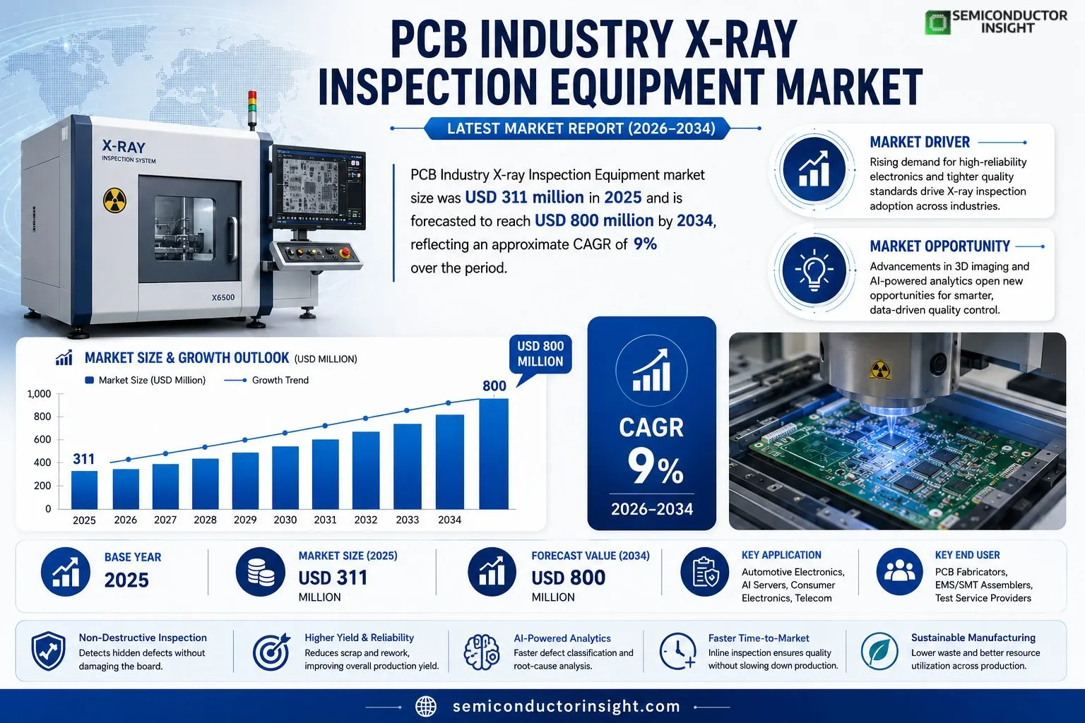
MARKET DRIVERS
Production Yield Pressure
Manufacturers are confronting tighter tolerance windows as component miniaturization accelerates. The need to detect hidden conductor breaches or voids before final testing forces many firms to upgrade to high‐resolution X‑ray systems, directly lifting demand for the PCB Industry X-ray Inspection Equipment Market. Companies that embed inline inspection report a measurable reduction in scrap rates, which translates into cost savings that outweigh the equipment premium.
Regulatory Scrutiny
Increasingly stringent safety and reliability standards in aerospace and automotive sectors compel suppliers to document every layer of a board. X‑ray inspection provides the evidence required for certification audits, making it a non‑negotiable step in the production flow for high‑value products. This regulatory push is a clear catalyst for broader adoption across midsize contract manufacturers.
➤ Operators that integrate automated X‑ray cells report up to a 30% improvement in defect‑traceability, enabling faster root‑cause analysis and shorter time‑to‑market.
As design cycles shrink, the ability to validate complex via structures in real time becomes a strategic advantage. Vendors that pair advanced imaging algorithms with AI‑driven analytics are positioning themselves as essential partners, reshaping the competitive landscape of the PCB Industry X-ray Inspection Equipment Market.
MARKET CHALLENGES
High Capital Outlay
State‑of‑the‑art X‑ray platforms carry price tags that can exceed several hundred thousand dollars, a barrier for smaller OEMs that operate on thin margins. Financing options remain limited, and the amortization period often extends beyond a single product lifecycle, discouraging rapid fleet upgrades.
Other Challenges
Technical Integration
Seamlessly linking X‑ray equipment to existing MES and SPC systems demands custom interfaces and skilled engineering support. The lack of standardized communication protocols leads to project delays and hidden integration costs, slowing market penetration.
MARKET RESTRAINTS
Skill Shortage
Operating high‑resolution X‑ray scanners and interpreting the resulting tomographic images requires specialized training. The pool of technicians proficient in both hardware calibration and defect classification remains shallow, prompting many plants to outsource inspectiona practice that adds lead time and reduces control.Vendors are attempting to mitigate this gap by offering remote support and automated analysis modules, yet the learning curve for new hires continues to constrain the speed at which organizations can fully leverage the technology.
MARKET OPPORTUNITIES
Emerging Form‑Factors
The rise of advanced packaging formatssuch as fan‑in wafer‑level packages and embedded component boardscreates a fresh demand for inspection solutions that can resolve sub‑100 µm features without dismantling the assembly. Early adopters are allocating budget to next‑generation X‑ray units that promise deeper penetration and finer voxel resolution.At the same time, the convergence of X‑ray imaging with machine‑learning anomaly detection opens a revenue stream for service‑based business models. Companies that bundle hardware with cloud‑hosted analytics can tap into recurring‑revenue contracts, expanding the addressable market beyond pure equipment sales.Geographically, mid‑size manufacturers in Southeast Asia are beginning to invest in inline X‑ray inspection to meet the quality expectations of Western OEMs. This regional shift presents a clear growth avenue for suppliers willing to establish localized support networks and flexible financing structures.
PCB Industry X-ray Inspection Equipment Market Trends
Shift Toward Integrated 3D Tomography
In 2025 the market produced roughly 2,300 units at an average price near US$148, reflecting both demand for higher resolution and capacity to scan larger boards. Customers in AI‑servers and automotive electronics are driving a migration from 2‑D inspection toward full‑volume 3‑D tomography. The added depth perception allows engineers to verify blind micro‑vias and HDI layer registration in a single pass, reducing the need for separate cross‑section analysis. This capability shortens time‑to‑repair, curtails field returns, and aligns with strict reliability specifications of data‑center and safety‑critical systems. As a result, OEMs are re‑architecting their platforms to accommodate larger detector panels and faster rotation stages, a shift that reshapes product road‑maps across the supply chain. Furthermore, the rise of multi‑chip module (MCM) architectures is compelling vendors to extend field‑of‑view beyond the traditional 150 mm limit, prompting a wave of engineering investments in larger‑area detectors and modular gantry designs. These developments are accelerating the shift from niche R&D tools to mainstream shop‑floor assets.
Other Trends
Supply Chain Consolidation
The prevailing “platform‑plus‑application” delivery model is consolidating component sourcing across the value chain. Tube manufacturers, detector suppliers and motion‑control firms are increasingly signing long‑term agreements with the three largest system integrators, which together control close to 40 % of 2025 revenue. This alignment secures stable availability of high‑voltage X‑ray tubes and flat‑panel detectors, mitigating the risk of production delays that historically plagued custom builds. At the same time, integrated service contracts that bundle calibration, radiation‑safety certification and AI‑software updates are lifting gross margins into the upper half of the 35‑55 % range. Companies that can synchronize hardware refresh cycles with customer takt‑time constraints are gaining repeat‑order leverage, especially in high‑volume automotive electronics lines where line‑side inspection must keep pace with sub‑second cycle times.
AI‑Enabled Defect Analytics
Downstream customers are moving from merely spotting defects to quantifying them for closed‑loop yield improvement. In AI‑server boards, statistical void‑distribution profiles are fed directly into Manufacturing Execution Systems, enabling automatic adjustment of solder paste volumes and reflow curves. This data‑driven feedback loop is prompting equipment makers to embed advanced machine‑learning models that differentiate genuine anomalies from scattering artefacts, thereby reducing false‑call rates. Vendors that expose APIs for seamless MES integration are seeing faster adoption in telecom and aerospace programs where traceability is mandatory. The convergence of high‑throughput 3‑D capture with AI‑based analytics is reshaping the value proposition of the PCB Industry X-ray Inspection Equipment Market, turning inspection from a compliance checkpoint into a strategic lever for cost reduction and reliability assurance.
COMPETITIVE LANDSCAPE
Key Industry Players
PCB Industry X‑ray Inspection Equipment: Competitive Overview
The market is dominated by a handful of vertically integrated OEMs that control the core X‑ray tube, detector, and motion‑control platform. ViTrox, Nordson and Omron command roughly one‑third of revenues, leveraging extensive service networks and recurring software licences to sustain high gross margins. Their platforms are characterised by modular architectures that enable rapid re‑configuration for large‑format boards used in AI‑servers and automotive electronics. This concentration forces smaller entrants to specialise in niche applicationssuch as high‑resolution 3 D tomography for aerospace PCBsor to differentiate through proprietary defect‑recognition algorithms that reduce false calls in dense HDI assemblies.Beyond the three leaders, a diverse cohort of manufacturers fills the mid‑tier and specialist segments. Viscom and Waygate Technologies (Baker Hughes) excel in inline inspection solutions for high‑volume SMT lines, while companies like Test Research Inc. (TRI) and XAVIS Co., Ltd. focus on offline, high‑precision inspection for low‑volume, high‑value substrates. European firms such as ZEISS and Saki Corporation bring advanced optics and metrology expertise, positioning themselves to capture premium‑price contracts in aerospace and defense. Asian playersincluding Unicomp Technology, Zhengye Technology, and Creative Electronbenefit from proximity to PCB fabs, offering cost‑effective platforms that are increasingly upgraded with AI‑enabled defect analytics. This layered competitive structure creates a spectrum of purchasing options, from turnkey enterprise platforms to boutique systems tailored to specific packaging technologies.
List of Key PCB Industry X‑ray Inspection Equipment Companies Profiled
- ViTrox
- Viscom
- Nordson
- Omron
- Unicomp Technology
- NIKON
- Waygate Technologies (Baker Hughes)
- Comet Yxlon
- Test Research Inc. (TRI)
- Seamark ZM
- Zhengye Technology
- ZEISS
- Saki Corporation
- XAVIS Co., Ltd.
- SEC
- Techvalley
- Goepel Electronic
- Scienscope
- SXRAY
- Creative Electron
Segment Analysis:
| Segment Category | Sub-Segments | Key Insights |
| By Type |
|
Inline X‑ray Inspection Equipment
|
| By Application |
|
Automotive Electronics
|
| By End User |
|
EMS/SMT Assemblers
|
| By Technology |
|
3D X‑ray Inspection
|
| By Production Scale |
|
Large‑volume Production
|
Regional Analysis: PCB Industry X-ray Inspection Equipment Market
North America
Federal standards in the United States now reference X‑ray inspection as a core component of quality assurance for critical electronics, while Canada’s CSA guidelines emphasize defect detection at sub‑micron levels. These regulations compel manufacturers to invest in higher‑resolution systems, accelerating market penetration among firms that previously relied on optical inspection alone.
The shift from discrete scanners to automated, conveyor‑integrated X‑ray modules reflects a broader industry appetite for line‑speed inspection. Early adopters cite improved defect localization and a drop in rework cycles, prompting adjacent suppliers to align their equipment interfaces with existing manufacturing execution systems.
Contract manufacturers prioritize solutions that combine high‑throughput imaging with intuitive analysis software, allowing engineers to flag anomalies without extensive training. Vendors that bundle AI‑driven defect classification see stronger loyalty, as clients value the predictive insights that translate to lower warranty costs.
A handful of North American firms dominate the high‑end segment, but recent joint ventures with Asian component suppliers are reshaping pricing structures. These collaborations enable price‑competitive offerings without compromising the performance expectations of tier‑one aerospace programs.
Europe
European manufacturers benefit from a dense network of research institutions that continuously refine X‑ray detection algorithms. The region’s emphasis on Industry 4.0 integration pushes suppliers to offer modular inspection cells that can be retrofitted into existing lines. Nations such as Germany and France are witnessing an upswing in demand from the renewable‑energy sector, where PCB reliability under extreme temperature swings is paramount. The outcome is a market that values precision engineering alongside scalable software solutions, encouraging vendors to develop region‑specific service packages.
Asia‑Pacific
The Asia‑Pacific corridor is characterized by rapid capacity expansion, especially in China, Taiwan, and South Korea. While cost considerations dominate early‑stage purchases, the surge in high‑value consumer electronics is prompting a migration toward more capable X‑ray systems. Local OEMs are increasingly looking beyond price, seeking equipment that can cope with multilayer boards and fine‑pitch components. This evolution is prompting players to establish regional R&D hubs, ensuring that product roadmaps align with the nuanced demands of Asian manufacturers.
South America
In South America, market growth is anchored by the automotive and telecommunications sectors, which are beginning to adopt stricter board‑quality standards. Brazilian firms, in particular, are investing in pilot projects that embed X‑ray inspection into the final assembly stage, aiming to reduce field failures in harsh operating environments. The strategic implication is a gradual shift from sporadic equipment purchases to longer‑term service contracts that include on‑site training and maintenance.
Middle East & Africa
The Middle East & Africa region shows a nascent but accelerating interest in X‑ray inspection, primarily driven by defense and oil‑&‑gas projects that cannot tolerate hidden solder defects. While the market remains price‑sensitive, major contracts often stipulate compliance with international safety standards, compelling buyers to opt for higher‑specification equipment. Service‑oriented business modelswhere vendors provide turnkey solutions and continuous performance monitoringare gaining traction as local operators recognize the cost advantages of preventing costly board failures in remote installations.
Report Scope
This market research report provides a comprehensive analysis of the PCB Industry X-ray Inspection Equipment Market , covering the forecast period 2026–2034. It offers detailed insights into market dynamics, technological advancements, competitive landscape, and key trends shaping the industry.
Key focus areas of the report include:
- Market Overview: The report begins with an overview outlining its current market scenario, key growth indicators, and industry transformation drivers. It discusses macroeconomic factors, demand–supply balance, regulatory landscape, and the strategic role of semiconductors in powering advancements across industries such as automotive, telecommunications, consumer electronics, and industrial automation.
- Market Size & Forecast: Historical data and future projections for revenue, unit shipments, and market value across major regions and segments.
- Segmentation Analysis: Detailed breakdown by product type, technology, application, and end-user industry to identify high-growth segments and investment opportunities.
- Regional Insights: Insights into market performance across North America, Europe, Asia-Pacific, Latin America, and the Middle East & Africa, including country-level analysis where relevant.
- Competitive Landscape: Profiles of leading market participants, including their product offerings, R&D focus, manufacturing capacity, pricing strategies, and recent developments such as mergers, acquisitions, and partnerships.
- Technology Trends & Innovation: Assessment of emerging technologies, integration of AI/IoT, semiconductor design trends, fabrication techniques, and evolving industry standards.
- Market Drivers & Restraints: Evaluation of factors driving market growth along with challenges, supply chain constraints, regulatory issues, and market-entry barriers.
- Stakeholder Insights: Insights for component suppliers, OEMs, system integrators, investors, and policymakers regarding the evolving ecosystem and strategic opportunities.
Primary and secondary research methods are employed, including interviews with industry experts, data from verified sources, and real-time market intelligence to ensure the accuracy and reliability of the insights presented.
FREQUENTLY ASKED QUESTIONS:
What is the current market size of PCB Industry X-ray Inspection Equipment Market?
-> PCB Industry X-ray Inspection Equipment Market was valued at USD 311 million in 2025 and is expected to reach USD 573 million by 2032, growing at a CAGR of 8.2% during the forecast period.
Which key companies operate in PCB Industry X-ray Inspection Equipment Market?
-> Key players include ViTrox, Viscom, Nordson, Omron, Unicomp Technology, NIKON, Waygate Technologies (Baker Hughes), Comet Yxlon, Test Research Inc. (TRI), Seamark ZM, Zhengye Technology, ZEISS, Saki Corporation, XAVIS Co., Ltd., SEC, Techvalley, Goepel Electronic, Scienscope, SXRAY, Creative Electron, among others.
What are the key growth drivers?
-> Key growth drivers include AI‑driven demand for higher layer counts and denser interconnects, rising reliability requirements in AI servers, high‑speed networking and automotive electronics, and the need for non‑destructive detection of hidden defects in multilayer HDI and substrate PCBs.
Which region dominates the market?
-> Asia holds the largest market share, driven by extensive PCB manufacturing bases in China, Japan, South Korea and emerging Southeast Asian countries.
What are the emerging trends?
-> Emerging trends include large‑format X‑ray systems, advanced tomographic 3D reconstruction, low‑dose imaging, and integration of AI/ML algorithms for automated defect recognition and root‑cause analysis.

Get Sample Report PDF for Exclusive Insights
Report Sample Includes
- Table of Contents
- List of Tables & Figures
- Charts, Research Methodology, and more...
 Download Sample Report PDF