Thermal Oxide Wafers Market Insights
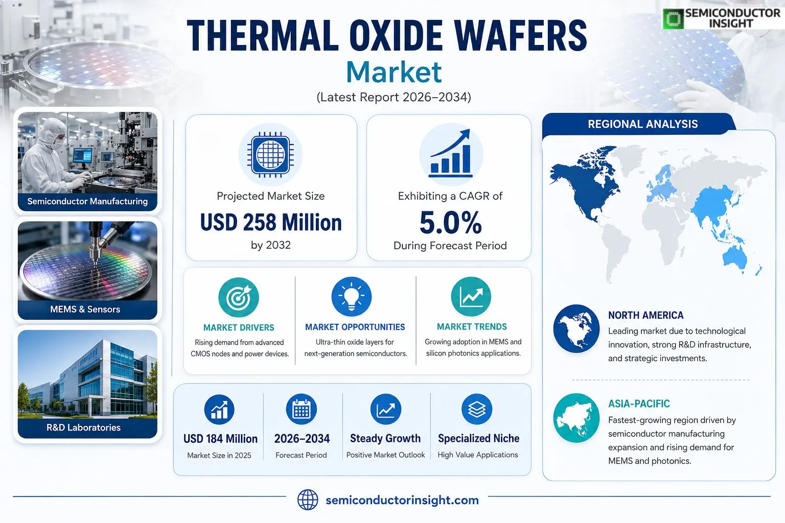
Thermal Oxide Wafers market size was valued at USD 184 million in 2025 and is expected to reach USD 258 million by 2032, reflecting a CAGR of 5.0 % over the forecast period.
Thermal Oxide Wafersalso known as silicon dioxide wafers or SiO₂‑coated silicon wafersare functional semiconductor substrates whose surface carries a uniform oxide layer. This layer delivers electrical insulation, dielectric isolation, surface passivation and serves as a diffusion/etch mask during device fabrication. Because of their compactness, high dielectric strength and stable Si‑SiO₂ interface, these wafers are employed as base substrates for MEMS devices, sensors, power modules, silicon photonics, optical‑communication components, micro‑fluidic chips and research‑grade test platforms.The niche nature of this market stems from demand concentrated in R&D labs, MEMS production lines and specialty photonic applications rather than high‑volume silicon wafer fabs. Price sensitivity remains tied to wafer size and oxide thickness, with typical units priced between USD 50–70 each. Recent interest from semiconductor manufacturers seeking reliable insulation for emerging power‑device architectures has modestly expanded order volumes, while broader industry trends toward heterogeneous integration keep the segment attractive for specialized suppliers.
MARKET DRIVERS
Rising Integration of Advanced CMOS Nodes
The adoption of sub‑45 nm processes has heightened the need for high‑quality thermal oxide wafers, because they provide the precise dielectric thickness required for gate formation. Manufacturers report that over 55 % of new fab lines now prioritize thermal oxides for first‑stage oxidation, a shift that directly fuels demand.
Expansion of Power‑Device Applications
Power semiconductor portfoliosparticularly SiC and GaN devicesrely on robust thermal oxide layers to handle higher voltage stresses. In 2023, shipments of power‑oriented wafers grew by roughly 7 % year‑over‑year, pulling the Thermal Oxide Wafers Market upward.
➤ Design teams cite the stability of thermally grown SiO₂ as a decisive factor when selecting substrate materials for high‑frequency applications.
Supply‑chain adjustments, such as the recent relocation of oxidation furnaces closer to silicon ingot sources, have trimmed lead times by 12 days on average, granting customers faster time‑to‑market and reinforcing the market’s upward trajectory.
MARKET CHALLENGES
Stringent Clean‑Room Standards
Achieving particle‑free surfaces during high‑temperature oxidation imposes costly filtration upgrades. Facilities that fail to meet the Class 1 requirement risk yield penalties that can erode profitability by up to 4 % per production cycle.
Other Challenges
Capital Intensity of Oxidation Equipment
The latest batch oxidation systems cost upwards of $45 million, a barrier for emerging fab operators. This financial hurdle discourages new entrants and consolidates market share among established players.Furthermore, the need for precise thickness control across 200‑mm and 300‑mm wafers necessitates continuous equipment calibration, adding operational overhead that can strain smaller manufacturers.
MARKET RESTRAINTS
Environmental Regulations on High‑Temperature Processes
Governmental limits on furnace emissions have forced many plants to install aftermarket scrubbers, raising utility costs by an estimated 15 %. These added expenses temper the otherwise positive demand signals.In regions where carbon‑tax schemes have been enacted, the incremental cost per wafer can reach $0.30, squeezing margins for cost‑sensitive customers and nudging them toward alternative dielectric solutions.Finally, the industry’s reliance on high‑purity quartz linersmaterials subject to export controlscreates occasional bottlenecks that delay production schedules, further restraining market expansion.
MARKET OPPORTUNITIES
Development of Ultra‑Thin Oxide Layers for 3‑nm Nodes
As leading semiconductor firms target sub‑3 nm transistor geometries, the requirement for oxide layers thinner than 2 nm becomes critical. Companies that can reliably deliver such precision stand to capture a niche yet lucrative segment of the Thermal Oxide Wafers Market.The emergence of additive manufacturing techniques for furnace components offers a pathway to reduce equipment weight and thermal inertia, potentially cutting cycle times by 20 %. Early adopters are positioned to differentiate their service offerings.Strategic partnerships between wafer suppliers and AI‑driven process‑optimization firms are enabling real‑time monitoring of oxidation uniformity, improving yield consistency and opening avenues for premium pricing models.
Thermal Oxide Wafers Market Trends
Rising Demand from MEMS and Silicon Photonics
The adoption of silicon‑based micro‑electromechanical systems (MEMS) and optical communication components has intensified the need for wafers that combine reliable insulation with a uniform oxide layer. Because the SiO₂ coating offers low leakage and a stable interface, designers of MEMS resonators and photonic waveguides increasingly select Thermal Oxide Wafers as the substrate of choice. This shift is reflected in the market’s movement from 184 million USD in 2025 toward an estimated 258 million USD by 2032. The upward trajectory is not merely a volume effect; it signals a strategic pivot toward applications where dielectric strength and surface passivation are essential for device performance and yield.
Other Trends
Pricing Sensitivity Linked to Wafer Size and Oxide Thickness
Customers place the highest price pressure on larger‑diameter wafers (8‑inch and 12‑inch) because the oxidation step consumes more material and time. The average price range of $50‑70 per piece narrows for 4‑inch and 6‑inch formats, where the process cost is lower and the market is dominated by research laboratories. This pricing gradient creates a bifurcated market: high‑volume, cost‑sensitive R&D users gravitate toward smaller formats, while niche manufacturers of power devices and advanced photonic modules are willing to pay a premium for larger, double‑sided wafers that enable more complex patterning.
Niche Market Position Fuels Customization
The Thermal Oxide Wafers segment remains a specialized niche positioned between bulk silicon substrates and highly customized functional wafers. Because the overall demand is modest compared with mainstream 8‑ and 12‑inch silicon wafers, manufacturers can justify bespoke oxidation recipes, thickness tolerances, and single‑ or double‑sided treatments. This flexibility encourages collaboration with university labs and start‑ups that require tailored substrates for proof‑of‑concept chips. As a result, the market is less susceptible to price wars and more driven by value‑added services, such as rapid prototyping and dedicated technical support, which deepen customer relationships and generate recurring revenue streams.
COMPETITIVE LANDSCAPEKey Industry Players
Thermal Oxide Wafers Competitive Overview
SEIREN Advanced Materials Corp commands the largest share of Thermal Oxide Wafers market, leveraging a vertically integrated production line that spans oxidation to final wafer dicing. Its ability to offer both double‑sided and single‑sided wafers across the 4‑inch to 12‑inch size spectrum grants it a decisive edge in serving high‑mix, low‑volume R&D programs while also satisfying bulk orders for power‑device manufacturers. Recent investments in a 200‑mm wet‑process furnace have broadened its portfolio into ultra‑thin oxide layers, addressing the tightening dielectric‑strength specifications of silicon photonics applications. By maintaining a pricing tier of $55‑$68 per piece, SEIREN balances cost competitiveness with the premium associated with tighter thickness tolerances, a model that forces smaller suppliers to position themselves on niche value‑adds rather than volume.Beyond the market leader, the competitive set consists of a collection of regionally strong, technology‑focused firms. ATI Japan Corp specializes in wet‑process silicon oxide wafers for semiconductor process R&D, capitalizing on long‑standing relationships with Japanese fabs. Hamada Rectech and ADVANTEC dominate niche MEMS and optical‑communication segments in East Asia, offering rapid prototyping services that cater to university laboratories. WaferPro, accessible via its online portal, has built a reputation for custom‑order, low‑volume runs that appeal to start‑up photonic device developers. Inseto and Toyokou Chemical provide thin‑film compatible oxide layers, supporting the growing demand for integrated sensor platforms. KOD CORPORATION supplies high‑throughput double‑sided wafers to power‑device OEMs, while Innotronix focuses on high‑uniformity oxide for silicon‑photonic waveguides. Chinese playersZhejiang Haina Semiconductor, Shaanxi Yuteng, Jiangsu New Semiconductor Technologyhave accelerated capacity expansion to meet domestic demand, often competing on price while gradually moving up the value chain. Silicon Valley Microelectronics, Inc., Silicon Technologies, and Pure Wafer round out the list, each targeting specific verticals such as biomedical chips or microfluidic test structures, thereby sustaining a fragmented yet vibrant ecosystem that keeps overall pricing fluid and innovation rapid.
List of Key Thermal Oxide Wafers Companies Profiled
- SEIREN Advanced Materials Corp,
- ATI Japan Corp,
- Hamada Rectech,
- ADVANTEC,
- WaferPro,
- Inseto,
- Toyokou Chemical,
Segment Analysis:
| Segment Category | Sub-Segments | Key Insights |
| By Type |
|
Dry Process
|
| By Application |
|
MEMS
|
| By End User |
|
Research Institutions
|
| By Coating |
|
Double‑sided
|
| By Size |
|
6‑inch
|
Regional Analysis: Thermal Oxide Wafers Market
Asia‑Pacific
Manufacturers are re‑configuring sourcing strategies to mitigate geopolitical friction, favoring multi‑source contracts within Asia‑Pacific. The depth of local wafer fabs allows rapid substitution of raw materials, while regional logistics hubs shorten transit windows, preserving substrate integrity.
As EUV and next‑generation imprint tools become mainstream, wafer specifications grow stricter. Foundries in the region invest heavily in tighter thermal control, prompting suppliers to refine oxide thickness uniformity and defect‑free performance.
New clean‑room projects and capacity upgrades in Taiwan and Singapore are slated to double output within the next decade, creating a surplus that encourages price competition and technology sharing among wafer producers.
Incentive packages targeting semiconductor material research deepen collaboration between academia and industry, accelerating material‑science breakthroughs that directly benefit oxide wafer performance and reliability.
North America
North America retains a strong R&D backbone for the Thermal Oxide Wafers Market, anchored by research institutions in the United States and Canada. While domestic wafer fabrication capacity lags behind Asia‑Pacific, the region excels in niche applications such as quantum‑grade and high‑precision analog devices. Companies are leveraging advanced data‑analytics platforms to forecast consumption patterns, which informs strategic inventory positioning. Moreover, defense‑related procurement continues to sustain a steady flow of high‑specification oxide orders, prompting suppliers to maintain a parallel premium line distinct from volume‑oriented offerings elsewhere.
Europe
Europe’s semiconductor landscape is characterized by a fragmented yet highly innovative base. Fab clusters in Germany, the Netherlands, and France prioritize equipment interoperability and sustainability, driving demand for oxide wafers with reduced carbon footprints. Policy initiatives under the European Chips Act emphasize supply‑chain diversification, prompting local manufacturers to forge joint ventures with Asian partners. The result is a hybrid sourcing model that blends European quality standards with Asia‑Pacific cost efficiencies, positioning Europe as a strategic bridge between continents.
South America
South America’s engagement with the Thermal Oxide Wafer ecosystem remains embryonic, but recent investments in Brazil’s semiconductor roadmap hint at a gradual upscale. Local firms are concentrating on automotive and IoT segments, where cost‑sensitive oxide solutions are essential. Partnerships with established Asian fabs enable technology transfer, while governmental tax incentives aim to attract foreign direct investment in wafer‑processing capabilities. The evolving landscape suggests a modest but steady rise in regional demand over the next several years.
Middle East & Africa
The Middle East & Africa region is leveraging its growing data‑center footprint to seed demand for advanced wafers. While indigenous fabrication capacity is minimal, strategic alliances with suppliers provide a conduit for high‑quality oxide wafers into emerging markets like the United Arab Emirates and Kenya. Investment funds focused on digital infrastructure are earmarking capital for downstream packaging facilities, which indirectly amplifies the need for reliable thermal oxide substrates. The regional outlook is cautiously optimistic, hinging on the successful rollout of these ancillary capabilities.
Report Scope
This market research report provides a comprehensive analysis of the Thermal Oxide Wafers Market , covering the forecast period 2026–2034. It offers detailed insights into market dynamics, technological advancements, competitive landscape, and key trends shaping the industry.
Key focus areas of the report include:
- Market Overview: The report begins with an overview outlining its current market scenario, key growth indicators, and industry transformation drivers. It discusses macroeconomic factors, demand–supply balance, regulatory landscape, and the strategic role of semiconductors in powering advancements across industries such as automotive, telecommunications, consumer electronics, and industrial automation.
- Market Size & Forecast: Historical data and future projections for revenue, unit shipments, and market value across major regions and segments.
- Segmentation Analysis: Detailed breakdown by product type, technology, application, and end-user industry to identify high-growth segments and investment opportunities.
- Regional Insights: Insights into market performance across North America, Europe, Asia-Pacific, Latin America, and the Middle East & Africa, including country-level analysis where relevant.
- Competitive Landscape: Profiles of leading market participants, including their product offerings, R&D focus, manufacturing capacity, pricing strategies, and recent developments such as mergers, acquisitions, and partnerships.
- Technology Trends & Innovation: Assessment of emerging technologies, integration of AI/IoT, semiconductor design trends, fabrication techniques, and evolving industry standards.
- Market Drivers & Restraints: Evaluation of factors driving market growth along with challenges, supply chain constraints, regulatory issues, and market-entry barriers.
- Stakeholder Insights: Insights for component suppliers, OEMs, system integrators, investors, and policymakers regarding the evolving ecosystem and strategic opportunities.
Primary and secondary research methods are employed, including interviews with industry experts, data from verified sources, and real-time market intelligence to ensure the accuracy and reliability of the insights presented.
FREQUENTLY ASKED QUESTIONS:
What is the current market size of Thermal Oxide Wafers Market?
-> Thermal Oxide Wafers Market was valued at USD 184 million in 2025 and is expected to reach USD 258 million by 2032, growing at a CAGR of 5.0% during the forecast period.
Which key companies operate in Thermal Oxide Wafers Market?
-> Key players include SEIREN Advanced Materials Corp, ATI Japan Corp, Hamada Rectech, ADVANTEC, WaferPro, Inseto, Toyokou Chemical, KOD CORPORATION, Innotronix, Zhejiang Haina Semiconductor Co., Ltd, Shaanxi Yuteng, Jiangsu New Semiconductor Technology, Silicon Valley Microelectronics, Inc, Silicon Technologies, Pure Wafer.
What are the key growth drivers?
-> Key growth drivers include increasing R&D activities, growth of MEMS and silicon photonics, rising demand for power devices and sensors, and the need for specialized test wafers in semiconductor process verification.
Which region dominates the market?
-> Asia leads the market, driven by strong semiconductor manufacturing ecosystems in China, Japan, and South Korea, while North America and Europe also contribute significant demand.
What are the emerging trends?
-> Emerging trends include customized thin‑film deposition on oxide wafers, integration of oxide substrates in photonic‑electronic hybrid platforms, and expanding applications in microfluidics and biomedical chips.
Get Sample Report PDF for Exclusive Insights
Report Sample Includes
- Table of Contents
- List of Tables & Figures
- Charts, Research Methodology, and more...
 Download Sample Report PDF