Fluorine Compound Etchant for Semiconductors Market Insights
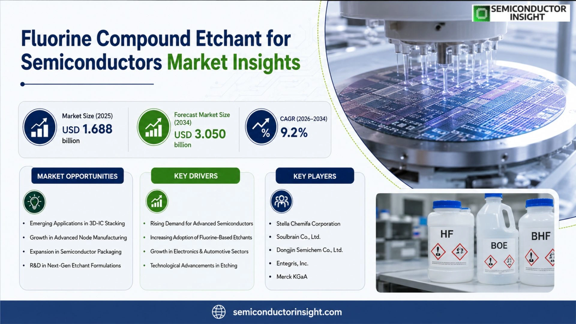
Fluorine Compound Etchant for Semiconductors market size was valued at USD 1.688 billion in 2025. Forecasts indicate growth from USD 1.688 billion in 2025 to USD 3.050 billion by 2032, reflecting a CAGR of 9.2%.
Fluorine compound etchants are high‑purity wet electronic chemicals that include electronic‑grade hydrofluoric acid, electronic‑grade ammonium fluoride, buffered oxide etchants, buffered hydrofluoric acid and specialty fluorine‑based formulations. They are used for oxide removal, surface preparation, contact‑hole cleaning, selective thin‑film stripping and metallization preparation throughout wafer fabrication and advanced packaging processes.
The market expands because semiconductor nodes are shrinking and three‑dimensional integration raises demand for predictable etch rates, low defectivity and tight impurity control. Japanese suppliers such as Stella Chemifa and Fujifilm dominate the high‑purity segment, while Korean firms like Soulbrain provide localized support for memory and logic fabs. Government programmes,including U.S. CHIPS incentives exceeding USD 39 billion and Europe’s Chips Act,strengthen fab capacity growth, driving higher consumption of
MARKET DRIVERS
Advances in Sub‑10nm Process Nodes
The push toward sub‑10nm transistors forces fabs to adopt etchants that can deliver atomic‑scale precision without compromising wafer yield. Fluorine Compound Etchant for Semiconductors Market players that engineer high‑selectivity chemistries are seeing immediate uptake because the alternative,multiple cleaning cycles,adds time and cost to already tight production windows.
Stringent Cleanroom Regulations
Regulatory bodies across North America and Asia have tightened limits on volatile organic compound (VOC) emissions. Fluorine‑based etchants, when formulated with low‑vapour‑pressure carriers, allow manufacturers to stay within compliance while maintaining etch rates, turning compliance into a market catalyst.
➤ Etchants capable of sub‑nanometer uniformity now serve as a decisive factor in winning high‑volume contracts.
These dynamics translate into a measurable shift in procurement budgets, with leading fabs reallocating up to 12 % of their chemical spend toward fluorine‑centric solutions. Investors tracking this trend are flagging the segment as a near‑term revenue generator.
MARKET CHALLENGES
Material Compatibility Constraints
While fluorine compounds excel in selectivity, they can aggressively attack certain low‑k dielectrics, leading to dielectric breakdown in advanced interconnect layers. Foundries must therefore qualify each etchant batch against a growing matrix of materials, inflating validation costs and extending time‑to‑market for new chemistries.
Other Challenges
Cost Sensitivity
Even though high‑performance fluorine etchants command premium pricing, many fab operators operate under razor‑thin margins. A 5 % rise in raw fluorine precursor costs has been reported to erode profitability across mid‑size fabs, prompting a search for cost‑balanced alternatives.
MARKET RESTRAINTS
Supply Chain Volatility for Fluorine Precursors
Geopolitical tensions affecting major fluorine‑producing regions have introduced unpredictable lead times for key feedstocks. Fab managers report occasional inventory gaps lasting two to three weeks, forcing them to hold higher safety stocks and increasing overall inventory carrying costs.
Environmental legislation mandating stricter disposal protocols for fluorinated waste adds another layer of operational complexity. Facilities must invest in specialized abatement units, a capital outlay that smaller players often cannot justify.
These supply‑side uncertainties dampen the willingness of new entrants to commit substantial R&D budgets toward fluorine‑based formulations, thereby slowing the influx of innovative products.
MARKET OPPORTUNITIES
Emerging Applications in 3D‑IC Stacking
The rise of three‑dimensional integrated circuits creates a niche where traditional wet etchants struggle to reach deep vias without causing damage. Fluorine compounds tailored for high‑aspect‑ratio etching can unlock reliable contact formation, opening a fresh revenue stream for suppliers that can certify process compatibility.
Concurrently, AI‑driven process control platforms are beginning to integrate real‑time chemical analytics, enabling dynamic adjustment of fluorine etchant concentrations. This synergy promises yield improvements of up to 8 %, positioning Fluorine Compound Etchant for Semiconductors Market as a strategic enabler of smart manufacturing.
Finally, partnerships between major semiconductor equipment OEMs and specialty chemical firms are accelerating the co‑development of bespoke etch modules. Early‑stage collaborations forecast a compound annual growth opportunity of roughly 6 % in the next five years, provided participants can navigate existing supply constraints.
Fluorine Compound Etchant for Semiconductors Market Trends
Shift Toward Buffered and Surfactant‑Modified Formulations
Fluorine Compound Etchant for Semiconductors Market is moving beyond the era of single‑component hydrofluoric acid. Fab engineers now demand solutions that combine precise impurity control with engineered wettability, prompting suppliers to blend HF with ammonium fluoride in buffered ratios and to embed surfactants that suppress particle adhesion. This chemistry evolution translates directly into tighter etch‑rate windows, lower defectivity, and higher downstream yield for advanced nodes. Because the cost of a single defect can outweigh the material price, manufacturers are willing to pay a premium for formulations that guarantee repeatable selectivity across silicon dioxide, silicon nitride, and metal‑containing layers. The trend reflects a broader industry push toward process robustness as device geometries contract and three‑dimensional integration becomes routine.
Other Trends
Supply‑Chain Lock‑In Through Qualified Service
Customers are increasingly evaluating vendors on the totality of the service package rather than on raw chemical price. Long‑term qualified supply agreements, on‑site blending capability, and rapid analytical support have become decisive criteria. Suppliers that can guarantee stable concentration during transport and provide real‑time particle‑count monitoring gain a strategic foothold, as any deviation can trigger costly re‑qualification cycles. This service orientation creates high switching barriers; once a fab embeds a particular etchant formulation into its process library, the qualification effort required for an alternative can run into months, reinforcing supplier stickiness and shaping the competitive dynamics of Fluorine Compound Etchant for Semiconductors Market.
Regional Consolidation Around East Asian Suppliers
Japan, South Korea, Taiwan, and mainland China dominate the supply landscape, each leveraging deep expertise in ultra‑pure fluorine chemistry and localized technical teams. Japanese firms lead in surfactant‑enhanced buffered systems, Korean players excel in rapid co‑development with memory fabs, while Taiwanese and Chinese companies have built logistics networks that ensure uninterrupted delivery to high‑volume fabs. This concentration is not merely a function of manufacturing capacity; it stems from accumulated knowledge in purification, analytics, and safety handling that few new entrants can replicate quickly. As global fab capacity expands and policy initiatives promote on‑shoring, the East Asian consortium is likely to tighten its grip, making regional collaboration a pivotal factor for any company seeking growth in this segment.
COMPETITIVE LANDSCAPE
Key Industry Players
Fluorine Compound Etchant for Semiconductors – Competitive Overview
The segment is dominated by a handful of Japanese and Korean firms that have cultivated deep expertise in high‑purity fluorine chemistry. Stella Chemifa leads the field with an extensive portfolio that spans single‑component HF, buffered oxide etchants (BOE/BHF) and surfactant‑enhanced formulations for SiO₂, Si₃N₄, TiN and advanced‑packaging films. Its business model couples long‑term qualified supply agreements with on‑site technical support, creating a barrier that locks customers into a trusted process platform. Kanto Chemical and Morita Chemical reinforce the Japanese foothold by supplying tightly controlled NH₄F‑based blends and custom‑ratio buffers, while Fujifilm leverages its semiconductor‑material legacy to deliver integrated wet‑process kits that align with sub‑10 nm node requirements. Daikin’s recent rollout of surfactant‑modified BHF‑U targets defect‑critical layers, underscoring how incremental formulation tweaks are transformed into competitive differentiation.
Beyond the core Japanese bloc, Korean specialists such as Soulbrain and ENF Technology have secured niche positions by aligning their product roadmaps with domestic memory and logic fabs, offering localized blending services and rapid response teams. In Greater China, Sunlit Fluoro & Chemical, Jiangyin Jianghua Microelectronics Materials and Shanghai Sinyang focus on high‑purity HF delivery and specialty SiN etchants, capitalising on the region’s aggressive fab expansion. European and global chemical giants,Solvay, BASF and Hitachi High‑Tech,enter the arena with broader wet‑process portfolios that embed circular‑economy services and advanced analytics, positioning themselves as one‑stop suppliers for multinational customers seeking both performance and ESG compliance. The overall structure therefore resembles an oligopoly where scale, purification know‑how and field service depth dictate market share, and new entrants typically gain footholds through a single formulation line before expanding their service envelope.
List of Key Fluorine Compound Etchant for Semiconductors Companies Profiled
- Stella Chemifa Corporation
- Kanto Chemical Co., Inc.
- Morita Chemical Industries Co., Ltd.
- Fujifilm Corporation
- Daikin Industries, Ltd.
- Soulbrain Co., Ltd.
- ENF Technology Co., Ltd.
- Solvay SA
- BASF SE
- Sunlit Fluoro & Chemical Co., Ltd.
- Jiangyin Jianghua Microelectronics Materials Co., Ltd.
- Shanghai Sinyang Semiconductor Materials Co., Ltd.
- Hitachi High‑Tech Corporation
- Asahi Kasei Corporation
- Merck KGaA
Segment Analysis:
| Segment Category | Sub-Segments | Key Insights |
| By Type |
|
Buffered Oxide Etchant is the leading sub‑segment because it balances aggressive oxide removal with controlled selectivity, enabling stable downstream deposition. – Provides predictable etch rates across multiple process nodes. – Reduces particle contamination through optimized HF/NH4F ratios. – Supports both front‑end and advanced‑packaging windows. |
| By Application |
|
Advanced Packaging drives the most strategic interest as manufacturers seek low‑defect, high‑selectivity etchants for 3‑D TSV and bumping. – Enables reliable dielectric removal in dense interconnect structures. – Aligns with ESG goals through surfactant‑modified formulations that lower waste. – Spurs co‑development partnerships with leading fab service providers. |
| By End User |
|
Foundries & Packaging Service Providers are the dominant end‑users because they integrate etchant supply into long‑term qualified programs, ensuring process stability. – High switching costs enforce sticky relationships. – Demand for localized technical service drives supply‑chain resilience. – Preference for customized formulations that meet strict impurity limits. |
| By Purity Level |
|
Ultra‑High Purity is critical for sub‑10 nm nodes where metal impurity and particle control directly affect yield. – Enables defect‑free interface conditioning. – Supports stringent ESG compliance through reduced waste streams. – Differentiates suppliers that invest in advanced filtration and analytics. |
| By Service Model |
|
Joint Development Programs are emerging as the most valuable model because they align supplier R&D with fab process roadmaps. – Accelerates time‑to‑market for specialty formulations. – Builds deep technical trust and co‑ownership of yield improvements. – Enables rapid response to node‑specific challenges. |
Regional Analysis: Fluorine Compound Etchant for Semiconductors Market
North America
The relentless push toward smaller process nodes forces etchant developers to tailor fluorine chemistry for higher selectivity, driving a wave of collaborative R&D programs that blend material science with lithography engineering.
Recent disruptions have prompted firms to diversify raw‑material sources, leading to regional hub‑and‑spoke models that keep critical intermediates closer to fabrication sites.
Tightened emissions standards in the United States encourage the adoption of closed‑loop etchant recycling, turning compliance considerations into a source of cost savings for large fabs.
Leading suppliers differentiate by offering on‑site technical support and rapid formulation tweaks, a service model that aligns closely with the high‑mix, low‑volume demands of advanced device prototypes.
Europe
European fabs emphasize sustainability, prompting etchant producers to prioritize low‑toxicity fluorine compounds that meet stringent REACH requirements. The region’s focus on modular clean‑room designs encourages suppliers to deliver standardized, plug‑and‑play chemistries, reducing integration risk for customers. Collaboration clusters around the Netherlands and Germany foster knowledge exchange, allowing smaller niche players to access larger scale production capabilities. As EU policy incentives target high‑performance computing, the demand for precision etching grows, steering manufacturers toward more refined process control solutions.
Asia‑Pacific
Asia‑Pacific’s rapid capacity expansion fuels a surge in demand for fluorine‑based etchants, particularly in Taiwan, South Korea, and China where leading foundries chase aggressive volume targets. The region benefits from a dense network of contract manufacturers that can quickly adapt formulations to local equipment quirks. However, divergent environmental regulations across jurisdictions force suppliers to maintain a flexible portfolio, balancing performance with compliance. The competitive intensity pushes vendors to offer aggressive pricing while still delivering the reliability required for high‑volume manufacturing.
South America
South America remains a niche market, with a handful of emerging semiconductor assembly lines that rely on imported etchants. Local players focus on cost‑effective supply chains, often partnering with North American distributors to secure stable inventories. Although the overall market size is modest, growing interest in IoT hardware manufacturing creates a modest upside, encouraging global suppliers to explore low‑volume, high‑margin contracts in the region.
Middle East & Africa
In the Middle East & Africa, the market is shaped by strategic investments in semiconductor fabrication hubs aimed at diversifying economies away from oil and minerals. Early‑stage projects prioritize robust chemical handling infrastructure, giving an opening to fluorine etchant manufacturers that can demonstrate safety and reliability. While demand is still embryonic, the region’s long‑term vision for a self‑sufficient supply chain could attract joint‑venture arrangements with established global players.
Report Scope
This market research report provides a comprehensive analysis of the Fluorine Compound Etchant for Semiconductors Market , covering the forecast period 2026–2034. It offers detailed insights into market dynamics, technological advancements, competitive landscape, and key trends shaping the industry.
Key focus areas of the report include:
- Market Overview: The report begins with an overview outlining its current market scenario, key growth indicators, and industry transformation drivers. It discusses macroeconomic factors, demand–supply balance, regulatory landscape, and the strategic role of semiconductors in powering advancements across industries such as automotive, telecommunications, consumer electronics, and industrial automation.
- Market Size & Forecast: Historical data and future projections for revenue, unit shipments, and market value across major regions and segments.
- Segmentation Analysis: Detailed breakdown by product type, technology, application, and end-user industry to identify high-growth segments and investment opportunities.
- Regional Insights: Insights into market performance across North America, Europe, Asia-Pacific, Latin America, and the Middle East & Africa, including country-level analysis where relevant.
- Competitive Landscape: Profiles of leading market participants, including their product offerings, R&D focus, manufacturing capacity, pricing strategies, and recent developments such as mergers, acquisitions, and partnerships.
- Technology Trends & Innovation: Assessment of emerging technologies, integration of AI/IoT, semiconductor design trends, fabrication techniques, and evolving industry standards.
- Market Drivers & Restraints: Evaluation of factors driving market growth along with challenges, supply chain constraints, regulatory issues, and market-entry barriers.
- Stakeholder Insights: Insights for component suppliers, OEMs, system integrators, investors, and policymakers regarding the evolving ecosystem and strategic opportunities.
Primary and secondary research methods are employed, including interviews with industry experts, data from verified sources, and real-time market intelligence to ensure the accuracy and reliability of the insights presented.
FREQUENTLY ASKED QUESTIONS:
What is the current market size of Fluorine Compound Etchant for Semiconductors Market?
-> Fluorine Compound Etchant for Semiconductors Market was valued at USD 1,688 million in 2025 and is expected to reach USD 3,050 million by 2032, growing at a CAGR of 9.2% over the forecast period.
Which key companies operate in Fluorine Compound Etchant for Semiconductors Market?
-> Key players include Stella Chemifa Corporation, Kanto Chemical Co., Inc., Morita Chemical Industries Co., Ltd., Fujifilm Corporation, Daikin Industries, Ltd., Soulbrain Co., Ltd., ENF Technology Co., Ltd., Solvay SA, BASF SE, Sunlit Fluoro & Chemical Co., Ltd., Jiangyin Jianghua Microelectronics Materials Co., Ltd., and Shanghai Sinyang Semiconductor Materials Co., Ltd.
What are the key growth drivers?
-> Key growth drivers include semiconductor fab capacity expansion, advanced logic and memory node scaling, rising demand for advanced packaging (3D TSV, HBM), governmental incentives such as the U.S. CHIPS Act and European Chips Act, and increasing ESG and fluorine‑waste recycling focus.
Which region dominates the market?
-> Asia‑Pacific dominates the market, driven by strong manufacturing bases in Japan, South Korea, China, and Taiwan, along with robust domestic supply chains and accelerating fab investments.
What are the emerging trends?
-> Emerging trends include development of high‑purity surfactant‑modified buffered formulations, on‑site blending services, circular economy initiatives for fluorine waste recovery, and customized etchants targeting niche advanced‑packaging applications such as heterogeneous integration and 3D NAND.
Get Sample Report PDF for Exclusive Insights
Report Sample Includes
- Table of Contents
- List of Tables & Figures
- Charts, Research Methodology, and more...
 Download Sample Report PDF