Silicon Oxide Wafers Market Insights
Silicon Oxide Wafers market size was valued at USD 184 million in 2025. The market is projected to grow from USD 184 million in 2025 to USD 258 million by 2032, exhibiting a CAGR of 5.0% during the forecast period.
Silicon Oxide Wafers, also known as silicon dioxide‑coated wafers, are functional semiconductor substrates that feature a uniform SiO₂ layer on a silicon base. This oxide film delivers electrical insulation, dielectric isolation, surface passivation and serves as a diffusion/etch mask during device fabrication. Because of its compactness, high dielectric strength and stable Si‑SiO₂ interface, the wafer is preferred for MEMS devices, sensors, power modules, silicon photonics, optical communication components and research‑grade test platforms.The niche nature of the market reflects its primary demand from R&D laboratories, MEMS manufacturers and specialty photonics producers rather than high‑volume silicon wafer lines. Recent collaborations between material suppliers and equipment makers have expanded process capabilities, while price sensitivity remains tied to wafer diameter and oxide thicknesstypically ranging from USD 50‑70 per piece. These dynamics shape investment decisions across semiconductor process development and emerging micro‑system applications.
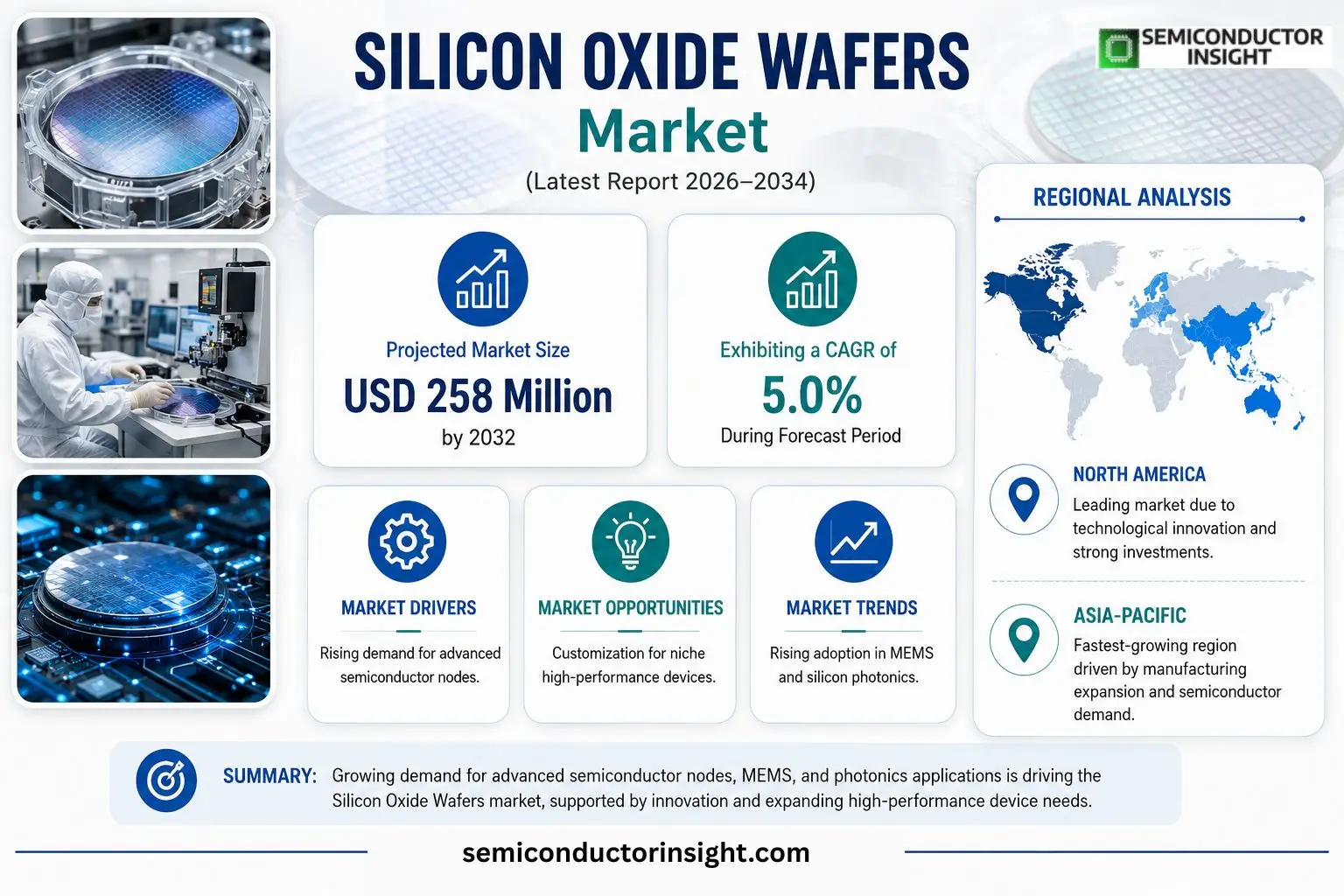
MARKET DRIVERS
Rising Demand for Advanced Semiconductor Nodes
The transition toward sub‑10 nm logic and memory architectures is forcing fab lines to adopt ultra‑thin dielectric layers. Silicon Oxide Wafers provide the thermal stability and low defect density required for high‑k/metal gate stacks, making them a preferred substrate for leading chipmakers. As yields improve, manufacturers are scaling wafer thickness to meet tighter design rules, directly boosting wafer volumes.
Expansion of Photonic and MEMS Applications
Emerging photonic integrated circuits and micro‑electromechanical systems rely on the insulating properties of silicon oxide to isolate optical waveguides and movable components. Growth in data‑center interconnects and automotive LIDAR has created a parallel market where silicon oxide wafers are a critical building block, prompting suppliers to diversify their product mixes.
➤ Manufacturers that can guarantee sub‑nanometer surface roughness are positioned to capture premium pricing tiers in both semiconductor and photonics segments.
Overall, the convergence of tighter scaling, new optical workloads, and the need for defect‑free interfaces is establishing a robust demand foundation for Silicon Oxide Wafers Market across multiple high‑value end‑use categories.
MARKET CHALLENGES
Stringent Quality Control Requirements
Achieving the required flatness and contamination thresholds demands sophisticated metrology and clean‑room infrastructure. Small deviations in particle count can translate into costly re‑work, discouraging entry by lower‑margin producers and compressing the supplier base.
Other Challenges
Supply‑Chain Vulnerabilities
Fluctuations in high‑purity quartz feedstock, combined with geopolitical constraints on semiconductor equipment, introduce lead‑time uncertainty that can stall production ramps for major clients.
MARKET RESTRAINTS
Capital‑Intensive Production Facilities
The equipment needed to grow and polish silicon oxide wafers to sub‑nanometer precision commands multi‑hundred‑million‑dollar investments. New entrants face prohibitive upfront costs, limiting competitive pressure and slowing price erosion.
Environmental Regulations
Strict emissions standards for chemical‑mechanical polishing and waste‑water treatment increase operating expenses. Facilities that cannot meet local compliance thresholds risk shutdowns, constraining supply in regions with tighter environmental oversight.
MARKET OPPORTUNITIES
Customization for Niche High‑Performance Devices
Clients developing quantum‑computing processors and neuromorphic chips are seeking wafer specifications that differ from mainstream logic lines. Tailored thicknesses, dopant profiles, and surface treatments create premium‑price segments where Silicon Oxide Wafers Market players can differentiate.
Geographic Expansion into Emerging Semiconductor Hubs
Regions such as Southeast Asia and Eastern Europe are receiving governmental incentives to build advanced fab capacities. Establishing local wafer production sites can reduce logistics costs and capture market share from legacy suppliers focused on traditional hubs.
Silicon Oxide Wafers Market Trends
Rising Adoption in MEMS and Silicon Photonics
The niche nature of the Silicon Oxide Wafer segment is being reshaped by intensified activity in micro‑electromechanical systems (MEMS) and silicon‑based photonic circuits. Engineers value the uniform SiO₂ layer for its ability to isolate circuitry while preserving low leakage, a prerequisite for high‑frequency MEMS resonators and low‑loss waveguides. As universities and corporate labs expand prototype programs, the demand curve shifts from occasional test pieces toward small‑batch production runs. This transition is not merely volume‑driven; it reflects a strategic move by device designers to embed reliable dielectric protection early in the fabrication flow, thereby reducing downstream rework. The consequence for suppliers is a need to tighten process control and offer rapid turnaround on custom thicknesses.
Other Trends
Pricing Sensitivity Tied to Wafer Size and Oxide Thickness
Price points for silicon oxide wafers cluster between $50 and $70 per unit, but the slope of the cost curve steepens when dimensions exceed 6‑inch or when double‑sided oxidation is specified. Buyers in the power‑device arena, which often require thicker oxides for voltage isolation, are willing to absorb a premium for tighter thickness tolerance. Conversely, MEMS developers focused on rapid prototyping favor the lower‑cost 4‑inch single‑sided options, even if that entails higher per‑unit defect risk. This pricing elasticity compels manufacturers to calibrate inventory between high‑margin specialty orders and volume‑oriented standard sizes, a balance that directly influences cash flow and capacity planning.
Application Portfolio Diversification
Beyond traditional semiconductor process R&D, the Silicon Oxide Wafer market is branching into biomedical chips, microfluidic platforms, and optical communication components. The stable Si‑SiO₂ interface supports bio‑compatible surface treatments, enabling sensor developers to integrate electrical read‑out with fluidic channels. In optical domains, the low‑loss nature of thermally grown oxide layers is critical for coupling light into silicon waveguides, prompting telecom equipment makers to source wafers with stringent roughness specifications. This broadened application base dilutes reliance on any single end‑user segment, offering manufacturers a more resilient revenue foundation. Companies that can align their product roadmaps with these emerging needs stand to capture incremental share without inflating production scale.
COMPETITIVE LANDSCAPEKey Industry Players
Silicon Oxide Wafers Competitive Overview
The market continues to revolve around a handful of vertically‑integrated suppliers that command both wafer‑fabrication capacity and a suite of value‑added coating services. SEIREN Advanced Materials Corp stands out as the de‑facto leader, leveraging a footprint of cleanrooms and a reputation for tight thickness control across 4‑ to 12‑inch formats. Its ability to bundle oxide deposition with downstream patterning keeps large OEMs and university labs locked into long‑term supply contracts, reinforcing a tier‑one concentration that limits price volatility. Smaller regional players tend to focus on niche thicknesses or specialty coatings, but the overall structure remains dominated by a few firms that can scale batch volumes while maintaining the uniformity required for MEMS and photonic applications.Beyond the flagship, a diverse set of manufacturers occupies distinct corners of the ecosystem. ATI Japan Corp and Hamada Rectech, for example, have cultivated strong relationships in the Japanese sensor segment, emphasizing double‑sided wafers for high‑precision micro‑fluidics. ADVANTEC and WaferPro pursue aggressive R&D pipelines, targeting emerging silicon photonics designs that demand ultra‑thin oxide layers. Companies such as Inseto, Toyokou Chemical, and KOD CORPORATION differentiate themselves through rapid‑turn custom orders for university research, while Zhejiang Haina Semiconductor and Shaanxi Yuteng provide cost‑effective bulk supplies for power‑device prototyping. This blend of scale‑driven and niche‑focused players creates a competitive backdrop where technological agility often outweighs sheer volume.
List of Key Silicon Oxide Wafers Companies Profiled
- SEIREN Advanced Materials Corp
- ATI Japan Corp
- Hamada Rectech
- ADVANTEC
- WaferPro
- Inseto
- Toyokou Chemical
- KOD CORPORATION
- Zhejiang Haina Semiconductor Co., Ltd
- Shaanxi Yuteng
- Silicon Valley Microelectronics, Inc
- Pure Wafer
- Silicon Technologies
- Jiangsu New Semiconductor Technology
Segment Analysis:
| Segment Category | Sub-Segments | Key Insights |
| By Type |
|
Dry Process
|
| By Application |
|
MEMS
|
| By End User |
|
Research Laboratories
|
| By Process |
|
Single‑sided
|
| By Coating |
|
Thin‑Film Oxide Coating
|
Regional Analysis: Silicon Oxide Wafers Market
Asia-Pacific
Fab expansions across Taiwan and South Korea have pushed output beyond the thresholds needed for emerging AI chips, thereby creating surplus capacity that can be redirected to specialty applications. Operators are retrofitting line‑side tooling to accommodate thinner oxide films, a move that enhances yield while positioning the region to serve niche demand curves without extensive capital outlay.
The proximity of raw‑material producers to wafer fabs reduces transit latency, a critical factor when handling high‑purity silicon oxide precursors. Regional trade agreements have streamlined customs procedures, allowing inventory buffers to shrink while maintaining continuity of supply even during seasonal demand spikes.
Collaborative research programs between leading universities and equipment manufacturers are pioneering atomic‑layer deposition techniques that promise sub‑nanometer control. These initiatives not only elevate performance benchmarks but also generate proprietary process IP that can be commercialized across the broader Silicon Oxide Wafers Market.
Tightening emissions standards in China and Japan are driving fabs toward greener chemistries and water‑recycling loops. Companies that integrate low‑impact oxide deposition processes gain regulatory goodwill and differentiate themselves in a market where sustainability credentials increasingly influence purchasing decisions.
North America
In North America, Silicon Oxide Wafers Market is shaped by a mature ecosystem of defense‑related semiconductor production and a burgeoning focus on heterogeneous integration. The United States leverages its advanced lithography base to demand wafers with exceptionally uniform oxide layers, a prerequisite for high‑density interconnects. While labor costs are higher than in Asia, the region compensates through relentless automation and a strong intellectual property framework that protects novel oxide deposition methods. Strategic partnerships between material suppliers and fab operators are emerging to address the growing need for low‑dielectric‑constant oxides in next‑generation processors, ensuring that North America retains a competitive edge despite a comparatively smaller production volume.
Europe
Europe’s contribution to Silicon Oxide Wafers Market rests on precision engineering and a regulatory environment that emphasizes product safety and environmental stewardship. German and Dutch fabs prioritize ultra‑clean process environments, enabling the production of wafers with minimal contaminant inclusiona factor critical for automotive and industrial IoT chips. The European Union’s emphasis on circular economy principles is prompting fabs to adopt wafer‑reuse schemes and recycle silicon oxide by‑products, thereby reducing material waste. Although the region’s overall capacity is modest, its focus on high‑value, low‑volume applications creates a niche that commands premium pricing.
South America
South America remains an emerging player in Silicon Oxide Wafers Market, with Brazil spearheading modest fab initiatives aimed at regional device assembly. The market’s growth is tempered by limited local supply chains, which necessitate imports of high‑purity silicon oxide precursors. Nevertheless, governmental incentives for semiconductor localization are beginning to attract foreign equipment vendors, laying the groundwork for a nascent manufacturing base. As local demand for consumer electronics and automotive electronics rises, the region is poised to transition from a pure importer to a modest producer of specialty wafers.
Middle East & Africa
The Middle East & Africa region offers a strategic logistics hub rather than extensive wafer fabrication capacity. Proximity to major shipping lanes enables rapid distribution of silicon oxide wafers to both Europe and Asia, positioning the region as a critical transshipment point. Emerging technology parks in the United Arab Emirates are courting R&D centers focused on materials science, which could eventually generate localized expertise in oxide layer engineering. While current market share is minimal, the combination of favorable tax regimes and investment in high‑tech infrastructure suggests a gradual shift from pure distribution to modest value‑added activities.
Report Scope
This market research report provides a comprehensive analysis of the Silicon Oxide Wafers Market , covering the forecast period 2026–2034. It offers detailed insights into market dynamics, technological advancements, competitive landscape, and key trends shaping the industry.
Key focus areas of the report include:
- Market Overview: The report begins with an overview outlining its current market scenario, key growth indicators, and industry transformation drivers. It discusses macroeconomic factors, demand–supply balance, regulatory landscape, and the strategic role of semiconductors in powering advancements across industries such as automotive, telecommunications, consumer electronics, and industrial automation.
- Market Size & Forecast: Historical data and future projections for revenue, unit shipments, and market value across major regions and segments.
- Segmentation Analysis: Detailed breakdown by product type, technology, application, and end-user industry to identify high-growth segments and investment opportunities.
- Regional Insights: Insights into market performance across North America, Europe, Asia-Pacific, Latin America, and the Middle East & Africa, including country-level analysis where relevant.
- Competitive Landscape: Profiles of leading market participants, including their product offerings, R&D focus, manufacturing capacity, pricing strategies, and recent developments such as mergers, acquisitions, and partnerships.
- Technology Trends & Innovation: Assessment of emerging technologies, integration of AI/IoT, semiconductor design trends, fabrication techniques, and evolving industry standards.
- Market Drivers & Restraints: Evaluation of factors driving market growth along with challenges, supply chain constraints, regulatory issues, and market-entry barriers.
- Stakeholder Insights: Insights for component suppliers, OEMs, system integrators, investors, and policymakers regarding the evolving ecosystem and strategic opportunities.
Primary and secondary research methods are employed, including interviews with industry experts, data from verified sources, and real-time market intelligence to ensure the accuracy and reliability of the insights presented.
FREQUENTLY ASKED QUESTIONS:
What is the current market size of Silicon Oxide Wafers Market?
-> Silicon Oxide Wafers Market was valued at USD 184 million in 2025 and is expected to reach USD 258 million by 2032, growing at a compound annual growth rate (CAGR) of 5.0% during the forecast period.
Which key companies operate in Silicon Oxide Wafers Market?
-> Key players include SEIREN Advanced Materials Corp, ATI Japan Corp, Hamada Rectech, ADVANTEC, WaferPro, Inseto, Toyokou Chemical, KOD CORPORATION, Innotronix, Zhejiang Haina Semiconductor Co., Ltd, Shaanxi Yuteng, Jiangsu New Semiconductor Technology, Silicon Valley Microelectronics, Inc, Pure Wafer, Silicon Technologies.
What are the key growth drivers?
-> Key growth drivers include increasing R&D activities, demand for MEMS and silicon photonics, growth in power device and sensor applications, and the need for reliable dielectric isolation and surface passivation in advanced semiconductor processes.
Which region dominates the market?
-> Asia leads the market due to strong manufacturing bases in China, Japan, and South Korea, as well as expanding research initiatives across the region.
What are the emerging trends?
-> Emerging trends include greater adoption of silicon oxide wafers for microfluidics, biomedical chips, and optoelectronic components, as well as the development of customized thin‑film processes to enhance dielectric performance.
Get Sample Report PDF for Exclusive Insights
Report Sample Includes
- Table of Contents
- List of Tables & Figures
- Charts, Research Methodology, and more...
 Download Sample Report PDF