Semiconductor Profilometer Market Insights
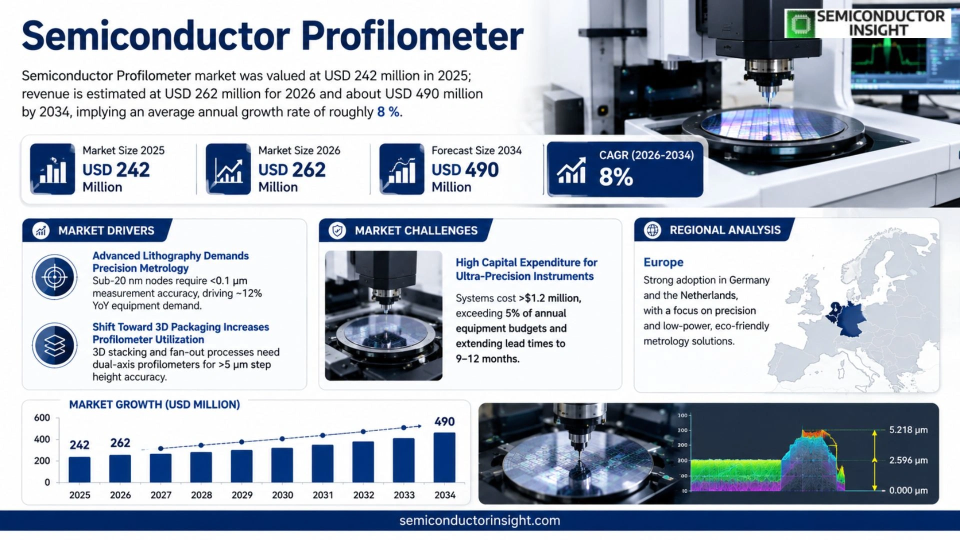
Global Semiconductor Profilometer market size was valued at USD 242 million in 2025; revenue is estimated at USD 262 million for 2026 and about USD 490 million by 2034, implying an average annual growth rate of roughly 8 %.
Semiconductor profilometers are precision metrology instruments used to capture surface morphology, step height, roughness, warpage and stress on wafers and related process samples. They serve both front‑end and back‑end manufacturing steps and fall into two principal families: contact stylus devices and non‑contact optical systems.
The expansion of advanced node production, higher demand for defect‑free packaging and increasing adoption of heterogeneous integration are pushing manufacturers toward more accurate metrology
MARKET DRIVERS
Advanced Lithography Demands Precision Metrology
The push for sub‑20 nm patterning forces manufacturers to adopt measurement tools that can resolve surface variations below 0.1 µm. Semiconductor Profilometer Market participants that provide sub‑nanometer vertical resolution are seeing order volumes rise by roughly 12 % year‑over‑year as fabs replace legacy interferometers.
Shift Toward 3D Packaging Increases Profilometer Utilization
Three‑dimensional stacking introduces top‑ography complexities not present in planar devices. Chip‑on‑wafer and fan‑out‑on‑panel processes generate step heights that exceed 5 µm, a range where conventional scatterometry loses accuracy. Vendors offering dual‑axis profilometers are capturing an estimated 8 % of new equipment spend in this segment.
➤ “Customers now treat metrology as a yield‑critical gate rather than a post‑production check,” notes a senior engineer at a leading foundry.
Beyond yield, the ability to feed real‑time surface data into process‑control loops shortens cycle time. Companies that embed this feedback capability report cycle reductions of up to three days, translating into tangible cost avoidance for high‑volume production lines.
MARKET CHALLENGES
High Capital Expenditure for Ultra‑Precision Instruments
State‑of‑the‑art profilometers command price tags north of $1.2 million, a barrier for midsize fabs seeking to modernize. When capital outlay exceeds 5 % of annual equipment budget, purchase decisions become protracted, extending lead times to 9‑12 months.
The financing landscape offers limited leasing options, prompting many operators to defer upgrades until older units reach end‑of‑life. This delay erodes the competitive edge of facilities that could otherwise benefit from tighter process windows.
Other Challenges
Talent Shortage
Operating and interpreting data from high‑resolution profilometers requires specialists with combined optics and semiconductor process expertise. Training pipelines have not kept pace with demand, resulting in vacancy rates approaching 18 % for relevant engineering roles.
MARKET RESTRAINTS
Stringent Calibration Standards
Regulatory bodies and industry consortia have codified calibration cycles that must be completed every six months. Non‑compliance triggers costly re‑qualification processes, discouraging smaller manufacturers from adopting the most advanced profilometers.
Furthermore, the need for certified reference standards adds an operational overhead of roughly 2 % of the instrument’s total cost each year, a figure that tightens profit margins for cost‑conscious operators.
These compliance pressures also limit the speed at which new measurement algorithms can be rolled out, slowing the diffusion of innovative analysis techniques across Semiconductor Profilometer Market.
MARKET OPPORTUNITIES
Integration with AI‑Driven Defect Detection
Machine‑learning platforms are now capable of correlating profilometer scans with defect patterns in real time. Vendors that bundle AI analytics with hardware claim yield improvements of 4‑6 % on 7 nm nodes, an incentive that could accelerate adoption across both legacy and leading‑edge fabs.
Another growth vector stems from the emergence of silicon‑photonic chips, where waveguide sidewall roughness directly impacts optical loss. Profilometers engineered for optical‑grade surface assessment are uniquely positioned to serve this nascent sub‑market.
Finally, the proliferation of “chip‑as‑a‑service” models encourages fabless designers to outsource metrology. Service providers equipped with portable, high‑speed profilometers can capture market share by offering on‑demand measurement contracts, creating a recurring revenue stream distinct from traditional equipment sales.
Semiconductor Profilometer Market Trends
Shift Toward Non‑Contact Optical Metrology
Semiconductor Profilometer Market is seeing a pronounced migration from traditional stylus‑based instruments to optical solutions that rely on interferometry, white‑light scanning, and confocal techniques. This transition is rooted in the need for higher throughput on 300 mm and larger wafers, where any physical contact risks contaminating delicate features. Optical platforms such as those offered by Keyence, Sensofar and the emerging Nanjing Aimey line deliver sub‑nanometer vertical resolution while preserving sample integrity, making them attractive for both front‑end fab lines and back‑end packaging stages. OEMs are augmenting their portfolios with hybrid modules that combine rapid 3‑D scanning with built‑in roughness analysis, thereby reducing the number of separate metrology tools a fab must acquire. The strategic implication is clear: vendors that can integrate high‑speed, non‑contact measurement with robust data analytics are likely to capture a larger share of new equipment spend.
Other Trends
Supply‑Chain Pressures on Core Components
Upstream suppliers of precision motion stages, stabilized laser sources and high‑sensitivity displacement sensors are encountering tighter lead times as demand for semiconductor‑grade metrology rises. Companies such as KLA and Bruker have invested in in‑house sensor development to mitigate reliance on external specialty manufacturers. This vertical integration not only secures component availability but also allows tighter control over calibration standards, a critical factor when measurement uncertainty must stay below a few picometers. The downstream effect is a modest uptick in unit prices, but manufacturers justify the premium by emphasizing lower total‑cost‑of‑ownership through reduced downtime and fewer calibration cycles.
Broadening Application Base Beyond Pure Wafer Metrology
Historically, profilometers were confined to wafer morphology checks, yet today their capabilities are being leveraged across advanced packaging, power‑device inspection and even display panel flattening. The rise of heterogeneous integration has introduced new topographies,such as through‑silicon vias and micro‑bumps,that demand both high‑resolution height mapping and lateral roughness metrics. Providers like Chotest Technology and Zhejiang Dexun are tailoring their systems with specialized software modules that fuse profilometry data with defect‑review workflows, enabling a single platform to support production monitoring and R&D hypothesis testing. This convergence creates cross‑selling opportunities and encourages fab managers to view Semiconductor Profilometer Market as a strategic enabler rather than a niche measurement expense.
COMPETITIVE LANDSCAPE
Key Industry Players
Semiconductor Profilometer Market – Competitive Overview
The market is dominated by a handful of large OEMs whose product portfolios span both contact stylus and non‑contact optical technologies. KLA Instruments leads the segment with a stylus line that couples sub‑nanometer displacement sensors to automated motion stages, delivering the resolution required for advanced wafer warpage and stress analysis. Bruker’s Dektak series complements KLA by offering interchangeable probes and extended scan strokes, making it attractive for both research labs and high‑volume fabs. Together, these incumbents command a substantial share of the $242 million 2025 market, leveraging deep integration with metrology software suites that lock customers into end‑to‑end measurement workflows. Their scale also translates into higher gross margins and the capacity to invest in next‑generation interferometric modules.
Beyond the tier‑one leaders, a diverse set of specialists competes on niche functionality and regional reach. Keyence provides 3D laser scanning microscopy that merges contour, roughness, and thickness data in a single non‑contact instrument, appealing to manufacturers focused on rapid inline inspection. Sensofar and Evident advance white‑light interferometry and confocal approaches, targeting precision‑critical applications such as advanced packaging and power device verification. Companies such as Chotest Technology, Nanjing Aimey Instrument Technology, and Zhejiang Dexun Intelligent Technology have introduced high‑speed optical scanners and cost‑effective solutions for emerging fab locations. European firms Polytec GmbH and LMI Technologies add expertise in vibration‑isolated platforms and handheld metrology, while regional players like Jiangsu Jinggong and Dongguan Pomeas fill the supply chain for mid‑tier equipment in China. This layered ecosystem creates competitive pressure on pricing, feature sets, and service models.
List of Key Semiconductor Profilometer Companies Profiled
- KLA Instruments
- Keyence Corporation
- Bruker Corporation
- Sensofar Metrology
- Evident Technology
- Chotest Technology
- Polytec GmbH
- LMI Technologies
- Nanjing Aimey Instrument Technology
- Zhejiang Dexun Intelligent Technology
- Jiangsu Jinggong Semiconductor Equipment
- Dongguan Pomeas Precision Instrument
- Chroma ATE
- Jiangsu JITRIOE
Segment Analysis:
| Segment Category | Sub-Segments | Key Insights |
| By Type |
|
Contact Profilometers
|
| By Application |
|
Production Metrology
|
| By End User |
|
Wafer Foundries
|
| By Measurement Principle |
|
Interferometric Profilometers
|
| By Product Model |
|
Floor‑standing Systems
|
Regional Analysis: Semiconductor Profilometer Market
Silicon Valley, Austin, and the Boston corridor host clusters where profilometer engineers collaborate with semiconductor designers. These hubs accelerate the translation of emerging lithography challenges into tailored measurement solutions, reinforcing the region’s role as a crucible for breakthrough metrology concepts.
A diversified component base, anchored by domestic optics and precision mechanics suppliers, cushions North America against global disruptions. This resilience enables manufacturers to maintain steady production cadences and meet the exacting tolerances demanded by leading chipmakers.
Clear standards from agencies such as the SEMATECH consortium streamline certification processes. Predictable compliance timelines give vendors confidence to invest in next‑generation profilometer architectures without fearing protracted approval delays.
The presence of several megafoundries creates a concentrated yet demanding client base. Their preference for integrated metrology suites drives providers to bundle hardware with advanced analytics, shaping the commercial model of the market.
Europe
European fabs, particularly in Germany and the Netherlands, emphasize precision and sustainability. Manufacturers are integrating profilometers with low‑power consumption modes to align with stringent EU environmental directives. Collaborative research programs funded by the Horizon Europe agenda foster cross‑border innovation, allowing smaller niche players to influence mainstream tool development. The market narrative here leans toward incremental efficiency gains rather than radical redesigns, reflecting the region’s cautious investment climate.
Asia‑Pacific
Asia‑Pacific’s rapid capacity expansion fuels a relentless search for measurement accuracy at ever‑smaller node sizes. Chinese and Taiwanese foundries, while operating under distinct policy environments, share a common appetite for high‑throughput profilometers that can keep pace with dense wafer schedules. Local OEMs are accelerating technology transfer partnerships with Western firms, creating hybrid solutions that blend cost competitiveness with sophisticated analytics.
South America
In South America, the market remains anchored by niche applications in specialty sensor production and aerospace component manufacturing. Companies prioritize robust, easy‑maintenance profilometer systems that can operate in varied climate conditions. The region’s investment trajectory is shaped by government incentives aimed at fostering advanced manufacturing clusters, encouraging firms to adopt precision metrology as a catalyst for broader industrial diversification.
Middle East & Africa
The Middle East & Africa region is gradually emerging as a hub for semiconductor research driven by sovereign wealth fund allocations toward technology diversification. Early‑stage pilot lines in the United Arab Emirates and South Africa are experimenting with compact profilometer platforms that offer scalability for future fab developments. Market participants view these initiatives as strategic footholds, anticipating a longer‑term transition from experimental to commercial deployment.
Report Scope
This market research report provides a comprehensive analysis of the Semiconductor Profilometer Market , covering the forecast period 2026–2034. It offers detailed insights into market dynamics, technological advancements, competitive landscape, and key trends shaping the industry.
Key focus areas of the report include:
- Market Overview: The report begins with an overview outlining its current market scenario, key growth indicators, and industry transformation drivers. It discusses macroeconomic factors, demand–supply balance, regulatory landscape, and the strategic role of semiconductors in powering advancements across industries such as automotive, telecommunications, consumer electronics, and industrial automation.
- Market Size & Forecast: Historical data and future projections for revenue, unit shipments, and market value across major regions and segments.
- Segmentation Analysis: Detailed breakdown by product type, technology, application, and end-user industry to identify high-growth segments and investment opportunities.
- Regional Insights: Insights into market performance across North America, Europe, Asia-Pacific, Latin America, and the Middle East & Africa, including country-level analysis where relevant.
- Competitive Landscape: Profiles of leading market participants, including their product offerings, R&D focus, manufacturing capacity, pricing strategies, and recent developments such as mergers, acquisitions, and partnerships.
- Technology Trends & Innovation: Assessment of emerging technologies, integration of AI/IoT, semiconductor design trends, fabrication techniques, and evolving industry standards.
- Market Drivers & Restraints: Evaluation of factors driving market growth along with challenges, supply chain constraints, regulatory issues, and market-entry barriers.
- Stakeholder Insights: Insights for component suppliers, OEMs, system integrators, investors, and policymakers regarding the evolving ecosystem and strategic opportunities.
Primary and secondary research methods are employed, including interviews with industry experts, data from verified sources, and real-time market intelligence to ensure the accuracy and reliability of the insights presented.
FREQUENTLY ASKED QUESTIONS:
What is the current market size of Semiconductor Profilometer Market?
-> Semiconductor Profilometer market size was valued at USD 262 million for 2026 and about USD 490 million by 2034, implying an average annual growth rate of roughly 8 %.
Which key companies operate in Semiconductor Profilometer Market?
-> Key players include KLA Instruments, Keyence, Bruker, Teledyne Vision Solutions, Polytec GmbH, Evident, Zygo Corporation, Chotest Technology, Zhejiang Dexun Intelligent Technology, Sensofar Metrology, LMI Technologies, Jiangsu Jinggong Semiconductor Equipment, Dongguan Pomeas Precision Instrument, Chroma ATE, Nanjing Aimey Instrument Technology, Jiangsu JITRIOE.
What are the key growth drivers?
-> Key growth drivers include rising demand for high‑precision morphology metrology in front‑end and back‑end semiconductor processes, expanding memory, logic and advanced packaging production, and the shift toward non‑contact optical profilometry for faster, non‑destructive measurements.
Which region dominates the market?
-> Asia dominates Semiconductor Profilometer market, driven by major wafer foundries and advanced packaging facilities in China, Japan, South Korea and Taiwan.
What are the emerging trends?
-> Emerging trends include integration of AI‑enabled data analytics for defect prediction, adoption of white‑light interferometry and confocal optics for higher resolution, and development of hybrid contact‑non‑contact systems to broaden application coverage.

Get Sample Report PDF for Exclusive Insights
Report Sample Includes
- Table of Contents
- List of Tables & Figures
- Charts, Research Methodology, and more...
 Download Sample Report PDF