Gallium Nitride Wafer CMP Equipment Market Insights
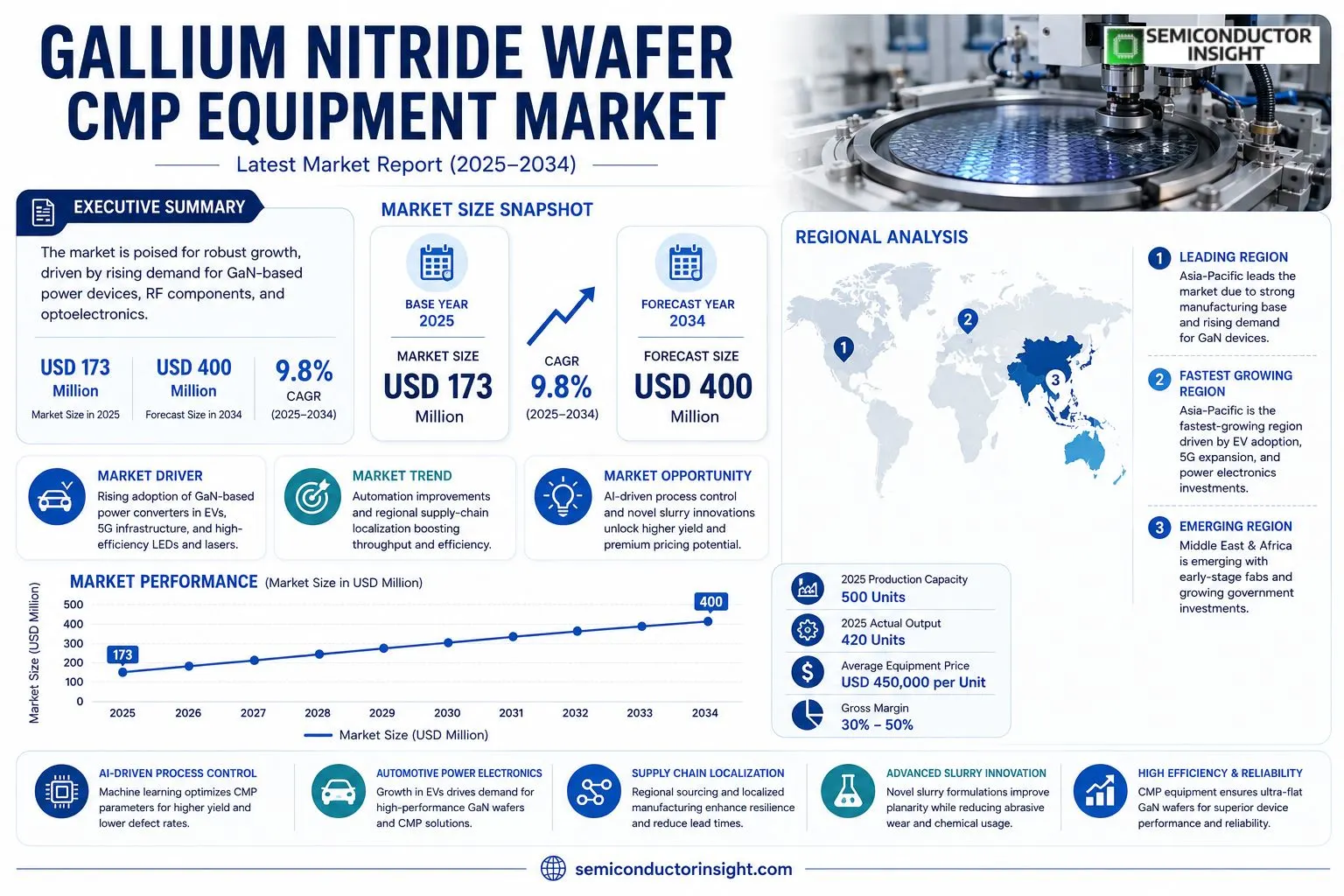
Gallium Nitride Wafer CMP Equipment market size was valued at USD 173 million in 2025. The market is expected to increase from USD 173 million in 2025 to approximately USD 400 million by 2034, reflecting an implied CAGR of roughly 9.8 % over the forecast horizon.
Gallium Nitride Wafer CMP (Chemical Mechanical Polishing) equipment comprises specialized machines that combine chemical etching with precise mechanical polishing to produce ultra‑flat GaN wafers. These systems remove surface irregularities while preserving wafer integrity, a prerequisite for high‑performance power‑semiconductor, RF, and optoelectronic devices.The expansion is fueled by rising adoption of GaN‑based power converters in electric‑vehicle drivetrains, growing deployment of RF components for 5G infrastructure, and increasing demand for high‑efficiency LEDs and lasers. In 2025 the production capacity reached about 500 units with an actual output of roughly 420 units, while average equipment pricing hovered around USD 450, 000 per unit and gross margins ranged between 30 % and 50 . Automation improvements and regional supply‑chain localizationparticularly across Asiaare enhancing throughput and reducing time‑to‑market for manufacturers.
MARKET DRIVERS
Rising Adoption of GaN Power Devices
Manufacturers of high‑efficiency power converters are increasingly specifying gallium nitride (GaN) substrates for their superior electron mobility and thermal performance. This shift forces wafer fabs to invest in advanced chemical‑mechanical planarization (CMP) tools that can reliably achieve sub‑nanometer surface uniformity. Investors watch these capital allocations as a clear signal of long‑term demand for CMP equipment tailored to GaN.
Expansion of 5G Infrastructure
The rollout of 5G networks accelerates the need for RF front‑ends that operate at higher frequencies, where GaN’s power density becomes a competitive advantage. Supply‑chain partners are therefore upgrading their polishing lines to reduce defect density, a prerequisite for meeting the stringent yield targets of telecom fabs. Efficiency gains in CMP throughput directly translate into faster time‑to‑market for 5G components.
➤ Equipment vendors reporting a 12 % YoY increase in orders for GaN‑specific CMP modules, reflecting tighter tolerances demanded by semiconductor producers.
Regulatory incentives in key regions, such as tax credits for low‑loss power devices, further stimulate capital spending on GaN wafer preparation. The ripple effect is a stronger pipeline for CMP manufacturers that can demonstrate compatibility with emerging GaN processes.
MARKET CHALLENGES
Complexity of GaN Material Properties
GaN’s high hardness and brittle nature make uniform planarization more difficult than conventional silicon. Operators must fine‑tune slurry chemistry and pad conditioning cycles, increasing process development time. Yield volatility can erode confidence among end‑users, slowing adoption of new CMP solutions.
Other Challenges
Supply‑Chain Fragility
The scarcity of high‑purity silicon carbide (SiC) pads, essential for GaN CMP, creates bottlenecks that can extend equipment lead times beyond twelve months. Companies without diversified sourcing strategies risk production downtime.Furthermore, the steep learning curve associated with integrating GaN‑focused CMP modules into existing fabs demands specialized training programs, adding a hidden cost that many mid‑size manufacturers find prohibitive.
MARKET RESTRAINTS
Capital Intensity of Upgrades
Upgrading to GaN‑compatible CMP equipment often requires multi‑million‑dollar investments in both hardware and cleanroom modifications. For fabs operating on thin margins, this financial barrier can delay or cancel planned expansions.
Limited Vendor Ecosystem
Only a handful of OEMs currently offer fully qualified GaN CMP solutions, limiting competitive pricing and slowing innovation diffusion. Buyers are forced to rely on a narrow set of suppliers, which can reduce bargaining power.The regulatory environment, while supportive of energy‑efficient technologies, still imposes strict compliance testing for new equipment. The time‑consuming certification process can act as a deterrent for rapid market entry.
MARKET OPPORTUNITIES
Emerging Automotive Power Electronics
Electric vehicles increasingly rely on GaN devices for on‑board chargers and inverter modules. This vertical creates a sizable, relatively untapped demand for CMP equipment that can deliver high‑yield wafers at scale. Early movers can capture design‑win partnerships with automotive OEMs.
Integration of AI‑Driven Process Control
Embedding machine‑learning algorithms into CMP tools enables real‑time adjustment of process parameters, reducing defect rates and improving cycle time. Vendors that can demonstrate measurable efficiency improvements are poised to command premium pricing.Finally, collaborative research programs between equipment manufacturers and academic institutions are generating novel slurry formulations that lower abrasive wear while maintaining surface planarity. These innovations promise to expand the addressable market size for GaN wafer CMP solutions over the next five years.
Gallium Nitride Wafer CMP Equipment Market Trends
Escalating Demand for High‑Power GaN Devices
The surge in power‑electronics and RF solutions built on gallium nitride is reshaping equipment requirements across the supply chain. End‑users such as 5G base‑station manufacturers, electric‑vehicle power‑train suppliers, and laser‑diode producers are mandating wafer flatness tighter than 10 nm RMS to preserve device efficiency. This stricter specification forces fab facilities to acquire CMP platforms capable of delivering repeatable results at high throughput, thereby lifting Gallium Nitride Wafer CMP Equipment Market. Manufacturers are responding by integrating advanced sensor‑fusion controls and AI‑driven polishing algorithms that reduce cycle time while preserving wafer integrity.
Other Trends
Shift Toward Double‑Side Polishing Solutions
Historically, single‑side machines dominated because early GaN wafers were limited to 100 mm. Today, the introduction of 150 mm and 200 mm substrates has exposed the inefficiency of processing each side separately. Double‑side equipment, which polishes both faces in a single loading, is cutting overall handling steps by roughly 30 percent and improving yield consistency. Suppliers in Japan and China have announced product roadmaps that prioritize double‑side capability, reflecting a clear market pivot.
Localization of the Supply Chain in Asia
Regional pressures to reduce lead times have accelerated the formation of localized component ecosystems for CMP tools. High‑purity slurries, precision CNC drives, and custom polishing pads are increasingly sourced from Asian vendors, shortening procurement cycles from months to weeks. This trend not only boosts equipment availability for domestic foundries but also raises the bar for after‑sales service, as local technicians can perform calibrations and firmware updates on‑site. Companies that embed regional partners into their value chain are gaining a competitive edge, particularly as government incentives in China and South Korea reward domestic semiconductor investment.
COMPETITIVE LANDSCAPE
Key Industry Players
Gallium Nitride Wafer CMP Equipment Competitive Overview
The market is anchored by a small group of multinational firms that command the majority of system integration capacity. Applied Materials leads with a broad portfolio that blends high‑precision CNC controls with proprietary slurry chemistry, enabling it to secure the bulk of high‑volume orders from semiconductor foundries in North America and Japan. DISCO Corporation follows closely, leveraging its long‑standing expertise in wafer processing to offer double‑side CMP platforms that meet the stringent flatness tolerances demanded by power‑device manufacturers. Tokyo Seimitsu and Ebara Technologies round out the top tier, each providing niche automation solutions that blend mechanical robustness with advanced sensor feedback, thereby capturing a sizable slice of the Asian mid‑range segment.Beyond the headline names, a constellation of specialized suppliers fuels innovation at the margins. Lapmaster Wolters GmbH focuses on ultra‑precise polishing pads and high‑speed spindle designs for 100 mm and 150 mm GaN wafers, catering to LED and laser device producers in Europe. KingTech and Dream Launch have emerged from China’s industrial parks with cost‑effective single‑side units that appeal to emerging power‑electronics assemblers. ENGIS and Galaxy Technology concentrate on slurry formulation and pad conditioning tools, roles that become critical as manufacturers strive for higher yields. Suzhou Fangda and other regional integrators provide localized service networks, reinforcing supply‑chain resilience in Southeast Asia and India.
List of Key Gallium Nitride Wafer CMP Equipment Companies Profiled
- Applied Materials
- DISCO Corporation
- Tokyo Seimitsu
- Ebara Technologies
- Lapmaster Wolters GmbH
- KingTech
- Dream Launch
- ENGIS
- Galaxy Technology
- Suzhou Fangda
- Revasum Inc.
- Okamoto Machine Tool Works
- Advanced CMP Solutions
Segment Analysis:
| Segment Category | Sub-Segments | Key Insights |
| By Type |
|
Double‑Side GaN CMP Equipment – Provides simultaneous polishing of both wafer faces, cutting cycle time. – Enhances uniformity across the wafer, critical for high‑performance power devices. – Aligns with automation trends, reducing manual handling and contamination risk. |
| By Application |
|
Power Semiconductor Devices – Demands ultra‑flat GaN wafers to sustain high voltage and current densities. – CMP quality directly influences device reliability and thermal performance. – Drives adoption of precision CMP solutions with tight defect control. |
| By End User |
|
Semiconductor Foundries – Require repeatable, high‑throughput CMP processes to meet volume production schedules. – Emphasize integration with fab automation and data analytics for yield optimization. – Prioritize equipment that supports multiple GaN wafer sizes and product families. |
| By Wafer Size |
|
200 mm GaN CMP Equipment – Aligns with industry shift toward larger wafers for cost‑per‑die reduction. – Offers enhanced polishing uniformity, essential for high‑power and RF applications. – Facilitates scaling of production lines while maintaining stringent surface quality. |
| By Process Mode |
|
Automated CMP – Delivers consistent polishing parameters across batches, reducing variability. – Integrates real‑time monitoring and closed‑loop control for defect mitigation. – Supports high‑mix, low‑volume production typical of emerging GaN device niches. |
Regional Analysis: Gallium Nitride Wafer CMP Equipment
Asia‑Pacific
Foundries in China and Vietnam have scaled CMP line capacity to accommodate larger wafer formats, reducing bottlenecks for gallium nitride substrate throughput. The expanded footprint allows equipment vendors to capture volume contracts that previously migrated to North America.
Recent logistics disruptions prompted firms to diversify sourcing of polishing pads and slurry chemicals, establishing regional inventories that mitigate lead‑time volatility and protect project timelines.
Government incentives for high‑efficiency power electronics encourage fabs to transition to gallium nitride platforms, indirectly stimulating demand for advanced CMP equipment tailored to low‑defect polishing.
Tier‑1 automotive suppliers are mandating tighter surface‑roughness specifications, compelling equipment manufacturers to embed AI‑driven process controls that adapt in real time to wafer variations.
North America
North America retains a sophisticated base of design houses that drive early‑stage adoption of gallium nitride wafers, yet the market is tempered by higher operating costs. Equipment vendors focus on premium service agreements that bundle predictive maintenance with software upgrades, catering to customers seeking to extend tool lifecycles. Collaborative research initiatives between universities and industrial labs sustain a pipeline of incremental technology improvements, especially in defect‑reduction algorithms. While volume growth lags behind Asia‑Pacific, the region’s emphasis on reliability and regulatory compliance ensures a steady flow of high‑margin contracts for specialized CMP solutions.
Europe
European fabs exhibit a cautious but methodical approach, prioritizing sustainability and material efficiency. Gallium Nitride Wafer CMP Equipment Market sees niche adoption in automotive power‑train projects where emissions standards drive a shift toward gallium nitride devices. Equipment providers are responding with modular tool architectures that allow incremental upgrades, aligning with the continent’s preference for capital‑expenditure flexibility. Strategic partnerships with local research institutes accelerate the development of low‑chemical‑consumption slurry formulations, reinforcing Europe’s reputation for environmentally conscious manufacturing.
South America
In South America, the market remains embryonic, constrained by limited local fabrication capacity. Nonetheless, regional telecom operators are piloting gallium nitride‑based amplifiers to improve network efficiency, creating a nascent demand for CMP tooling. Vendors are leveraging indirect sales channels and offering training programs to build technical expertise, laying the groundwork for future expansion as government incentives for high‑performance electronics take shape.
Middle East & Africa
The Middle East & Africa region is characterised by exploratory investments, driven primarily by sovereign wealth funds allocating capital to next‑generation semiconductor ecosystems. Early‑stage test beds are emerging in the United Arab Emirates and South Africa, where academic collaborations explore gallium nitride wafer handling. Equipment manufacturers view these initiatives as footholds for long‑term market entry, supplying pilot‑scale CMP units coupled with knowledge‑transfer services to nurture local capabilities.
Report Scope
This market research report provides a comprehensive analysis of the Gallium Nitride Wafer CMP Equipment Market , covering the forecast period 2026–2034. It offers detailed insights into market dynamics, technological advancements, competitive landscape, and key trends shaping the industry.
Key focus areas of the report include:
- Market Overview: The report begins with an overview outlining its current market scenario, key growth indicators, and industry transformation drivers. It discusses macroeconomic factors, demand–supply balance, regulatory landscape, and the strategic role of semiconductors in powering advancements across industries such as automotive, telecommunications, consumer electronics, and industrial automation.
- Market Size & Forecast: Historical data and future projections for revenue, unit shipments, and market value across major regions and segments.
- Segmentation Analysis: Detailed breakdown by product type, technology, application, and end-user industry to identify high-growth segments and investment opportunities.
- Regional Insights: Insights into market performance across North America, Europe, Asia-Pacific, Latin America, and the Middle East & Africa, including country-level analysis where relevant.
- Competitive Landscape: Profiles of leading market participants, including their product offerings, R&D focus, manufacturing capacity, pricing strategies, and recent developments such as mergers, acquisitions, and partnerships.
- Technology Trends & Innovation: Assessment of emerging technologies, integration of AI/IoT, semiconductor design trends, fabrication techniques, and evolving industry standards.
- Market Drivers & Restraints: Evaluation of factors driving market growth along with challenges, supply chain constraints, regulatory issues, and market-entry barriers.
- Stakeholder Insights: Insights for component suppliers, OEMs, system integrators, investors, and policymakers regarding the evolving ecosystem and strategic opportunities.
Primary and secondary research methods are employed, including interviews with industry experts, data from verified sources, and real-time market intelligence to ensure the accuracy and reliability of the insights presented.
FREQUENTLY ASKED QUESTIONS:
What is the current market size of Gallium Nitride Wafer CMP Equipment Market?
-> Gallium Nitride Wafer CMP Equipment Market was valued at USD 173 million in 2025 and is expected to reach USD 331 million by 2032, reflecting a CAGR of 9.9% during the forecast period.
Which key companies operate in Gallium Nitride Wafer CMP Equipment Market?
-> Key players include Applied Materials Inc., Ebara Technologies Inc., DISCO Corporation, Revasum Inc., Tokyo Seimitsu, Okamoto Machine Tool Works, Lapmaster Wolters GmbH, Dream Launch, KingTech, ENGIS, Galaxy Technology, Suzhou Fangda.
What are the key growth drivers?
-> Key growth drivers include the rising demand for high‑performance power and optoelectronic devices, the need for precise planarization of GaN wafers, increased automation and process repeatability, regional supply‑chain localization especially in Asia, and expanding applications in 5G, electric vehicles and next‑generation power electronics.
Which region dominates the market?
-> Asia dominates Gallium Nitride Wafer CMP Equipment Market, driven by strong manufacturing bases in Japan, China, and South Korea and growing local supply‑chain support.
What are the emerging trends?
-> Emerging trends include advanced automation of CMP processes, integration of AI for process control, development of higher‑throughput CMP systems, and increased focus on equipment localization to meet regional demand in fast‑growing semiconductor hubs.

Get Sample Report PDF for Exclusive Insights
Report Sample Includes
- Table of Contents
- List of Tables & Figures
- Charts, Research Methodology, and more...
 Download Sample Report PDF