Protective Coating for Semiconductor Fabrication Equipment Market Insights
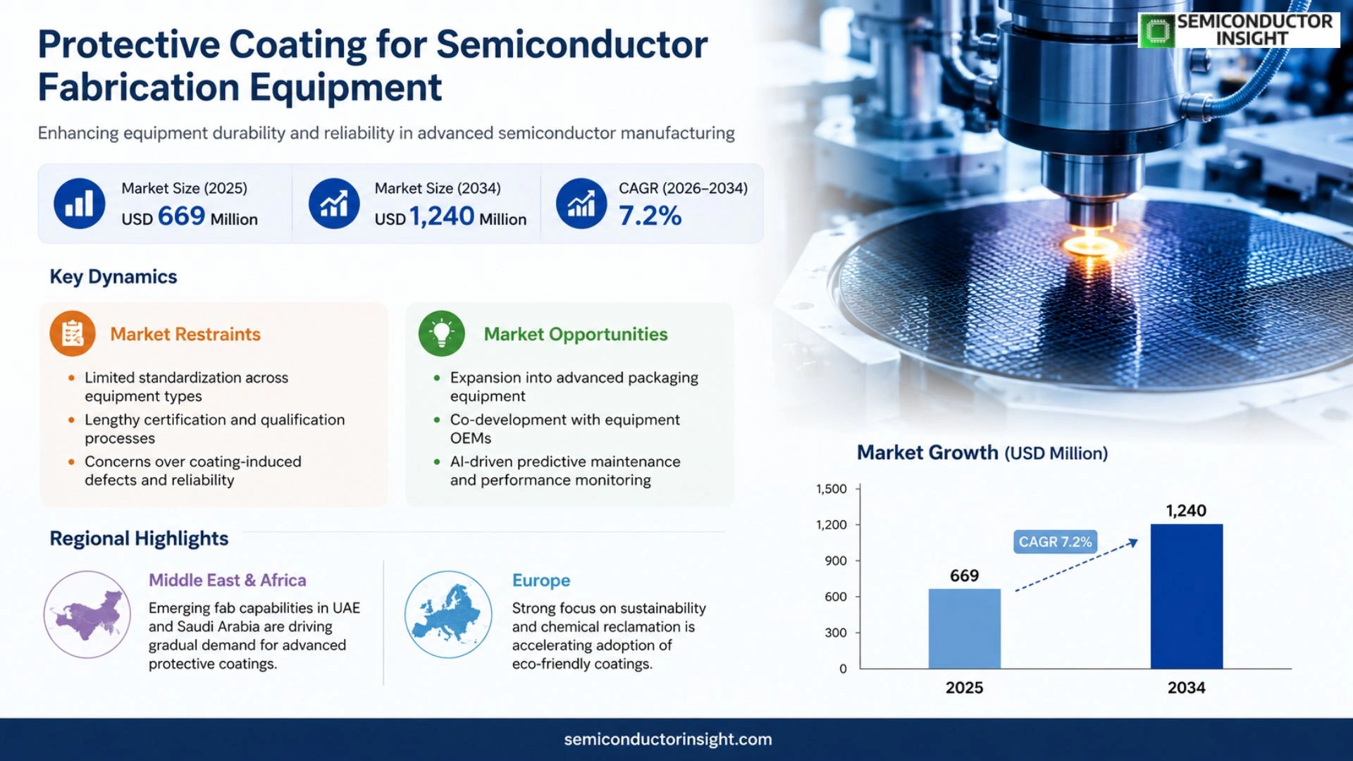
Protective Coating for Semiconductor Fabrication Equipment market is projected to grow from USD 669 million in 2025 to USD 1,240 million by 2034, exhibiting a CAGR of 7.2% during the forecast period.
Protective coating refers to engineered thin‑film or multilayer surfaces applied to semiconductor fabrication equipment such as etch chambers, showerheads, electrostatic chucks, liners and ceramic windows. These coatings,primarily ceramic‑based or metal‑alloy formulations,shield critical components from aggressive plasma chemistries, abrasive particles and thermal cycling, thereby extending part life, reducing contamination risk and preserving process yield.
The harsh environment of silicon wafer manufacturing accelerates wear on chamber components, making regular recoating essential for high‑volume fabs seeking consistent device performance.
MARKET DRIVERS
Increasing Demand for Equipment Longevity
Fabrication tools now operate at higher throughput to meet the push for advanced nodes, and each minute of downtime translates into measurable revenue loss. Operators are therefore investing in Protective Coating for Semiconductor Fabrication Equipment Market solutions that extend the service life of critical components by up to 30 %, reducing the frequency of costly part replacements.
Stringent Contamination Control Standards
Regulatory bodies and leading fabs have tightened particle‑count limits on wafer‑processing chambers. Innovative coating chemistries that create chemically inert, low‑shedding surfaces directly address these limits, allowing manufacturers to maintain yield levels while scaling to finer geometries.
➤ “A robust coating layer is the silent workhorse that keeps high‑precision tools in production longer without compromising cleanliness.”
Beyond reliability, the coating market benefits from the growing adoption of high‑k metal gate and EUV lithography platforms, both of which impose harsher plasma environments. Suppliers that can tailor film thickness and adhesion properties are gaining traction among equipment OEMs seeking to safeguard their next‑generation portfolios.
MARKET CHALLENGES
Compatibility with Emerging Process Chemistries
New etchants and photoresists introduce solvents that were not considered in legacy coating specifications. Aligning the protective layer’s resistance profile with these aggressive chemicals requires iterative testing, which can extend development cycles and increase upfront R&D spend.
Other Challenges
Cost‑Sensitivity of High‑Volume Manufacturers
While the long‑term savings of protective coatings are compelling, many fabs operate on razor‑thin margins. The incremental expense of applying a premium coating must be justified within a single production run, prompting buyers to demand transparent ROI models.
MARKET RESTRAINTS
Limited Standardization Across Equipment Types
Coating processes vary widely between deposition, etch, and inspection tools, yet industry guidelines remain fragmented. This lack of unified standards forces each equipment vendor to develop bespoke solutions, slowing broader market adoption.
Additionally, certification requirements for cleanroom compatibility often involve lengthy qualification phases. Fab managers may defer coating upgrades until a new tool generation arrives, creating a lag between technology readiness and field implementation.
Finally, the perception that coating application can introduce hidden defects,such as micro‑cracks under thermal cycling,remains a barrier. Overcoming this trust gap necessitates robust field data and transparent performance metrics.
MARKET OPPORTUNITIES
Expansion into Advanced Packaging Equipment
As semiconductor manufacturers shift focus toward 2.5‑D/3‑D integration, the protective coating market can leverage its core capabilities to address the unique wear patterns of wafer‑level packaging tools. Early adopters stand to secure differentiated positioning in a high‑value niche.
Another promising avenue lies in partnership models where coating providers collaborate directly with equipment OEMs during the design phase. Co‑engineered solutions that embed protective layers into the tool architecture can reduce retro‑fit costs and accelerate time‑to‑market.
Finally, the rise of AI‑driven predictive maintenance opens a data‑rich environment for coating performance monitoring. Integrating sensor analytics with coating durability models enables customers to schedule re‑coating events precisely, converting a traditional maintenance expense into a value‑added service.
Protective Coating for Semiconductor Fabrication Equipment Market Trends
Increasing Adoption of Ceramic Plasma‑Spray Coatings
The abrasive atmosphere inside etch and deposition chambers forces manufacturers to replace component surfaces more often, eroding productivity. Ceramic plasma‑spray formulations now dominate because they combine high thermal stability with resistance to fluorine‑rich chemistries. Installations that previously relied on metal alloys are switching to ceramic layers, which cut particle generation by a noticeable margin. This transition matters for fab owners: longer component lifetimes translate directly into higher equipment uptime and lower clean‑room downtime. Moreover, the wider availability of high‑purity yttrium‑based powders shortens qualification cycles, allowing OEMs to certify new coating runs faster than before. Service firms that can deliver consistent thickness and adhesion are gaining a strategic edge, as fab managers prioritize vendors that demonstrate reproducible performance across multiple tool generations.
Other Trends
Shift Toward Thin‑Film Multilayer Coatings
While plasma‑spray remains the workhorse for bulk protection, design teams are layering thin‑film PVD/ALD stacks over the base coating to address particle shedding at the nanoscale. These hybrid structures create a densified barrier that tolerates rapid temperature swings during high‑throughput cycles. The added complexity is justified by the fact that advanced logic nodes demand tighter contamination budgets; even a marginal reduction in sub‑micron debris can improve yield on 3‑nm processes. Companies that couple plasma‑spray expertise with in‑house ALD capabilities are positioning themselves as end‑to‑end solution providers, offering package‑level qualification data that simplifies the fab’s material approval workflow. This convergence is reshaping the competitive landscape, encouraging smaller specialists to merge or partner with larger service houses to broaden their technology portfolio.
Regional Consolidation of Service Providers
North America, Europe, and Asia‑Pacific each exhibit distinct supply‑chain dynamics, yet all are seeing a consolidation of coating service firms around a handful of multinational players. In North America, the top five providers capture roughly two‑thirds of the revenue, leveraging proximity to major fab hubs and a mature regulatory framework. European outfits benefit from strong standards on material traceability, which appeals to customers pursuing ultra‑low‑contamination processes. Asian providers, meanwhile, are expanding capacity to support the continent’s growing fab count, focusing on rapid turnaround and localized powder sourcing. The net effect is a market where regional expertise is bundled with global scale, forcing new entrants to differentiate through niche material innovations or ultra‑responsive field service. For customers, this shift means fewer but more capable partners, which can streamline contract negotiations and reduce the overhead associated with managing multiple vendors.
COMPETITIVE LANDSCAPE
Key Industry Players
Protective Coating Services: Competitive Dynamics Across Global Fab Equipment Market
The market is dominated by a handful of vertically integrated firms that combine proprietary plasma‑spray formulations with on‑site recoating capabilities. KoMiCo (USA) leverages a broad ceramic‑powder portfolio and maintains a network of service bays near major fabs, enabling it to capture roughly one‑third of global revenue despite intense price pressure. UCT (Ultra Clean Holdings) follows a similar model, differentiating through rapid turnaround times that align with the tight downtime windows of etch and deposition tools. TOCALO, Entegris and Oerlikon Balzers round out the top five, each holding a strategic mix of OEM contracts and long‑term service agreements that lock in recurring income. This concentration reflects the high barrier to entry posed by the need for clean‑room certification, advanced powder handling, and deep technical expertise to qualify coatings on high‑value equipment.
Beyond the leading tier, a diverse set of niche specialists sustains the market’s breadth. Companies such as Beneq and Cinos focus on emerging ALD‑compatible thin‑film stacks, positioning them for growth as fabs migrate to higher‑density nodes. Regional players,including Mitsubishi Chemical’s Cleanpart unit in Japan, FM Industries in Europe, and Pentagon Technologies in North America,pursue market share by tailoring formulations to local process chemistries and offering flexible financing models. Smaller innovators like Frontken Corporation, Hansol IONES, and DFtech exploit gaps in specialty coatings for electrostatic chucks and shield covers, where incremental performance gains translate into measurable yield improvements. Their agility allows quick adoption of new material chemistries such as fluorinated yttrium oxides, reinforcing the overall ecosystem’s resilience.
List of Key Protective Coating for Semiconductor Fabrication Equipment Companies Profiled
- KoMiCo
- UCT (Ultra Clean Holdings, Inc.)
- TOCALO Co., Ltd.
- Entegris
- Oerlikon Balzers
- Beneq
- Cinos
- Pentagon Technologies
- Mitsubishi Chemical (Cleanpart)
- FM Industries
- SilcoTek
- Frontken Corporation Berhad
- Hansol IONES
- DFtech
- Value Engineering Co., Ltd.
Segment Analysis:
| Segment Category | Sub-Segments | Key Insights |
| By Type |
|
Ceramic Coating is the predominant type because it offers superior plasma resistance and longevity in harsh process environments. – Provides excellent barrier against abrasive etchants, extending component life. – Enables stable thermal performance for high‑temperature chambers. – Aligns with industry demand for low‑particle emission surfaces. |
| By Application |
|
Etching Equipment leads the application segment as it faces the most aggressive chemistries and plasma exposure. – Protective layers mitigate premature wear of chamber walls and showerheads. – Reduces particle generation, crucial for device yield. – Supports the shift toward denser, multi‑pattern etch processes. |
| By End User |
|
Fab Equipment Manufacturers dominate because they integrate coating services directly into equipment supply contracts. – Require consistent coating quality to meet stringent uptime targets. – Favor suppliers with close proximity to major semiconductor clusters. – Value collaborative development for next‑generation plasma‑resistant materials. |
| By Coating Material |
|
Oxide‑based Systems remain the core material class due to their proven durability and ease of processing. – Offer high hardness while maintaining thermal stability. – Provide a versatile platform for integrating dopants that improve plasma resistance. – Serve as the baseline from which newer fluoride‑based innovations evolve. |
| By Technology |
|
Plasma Spray continues to dominate the technology landscape as it delivers high throughput and robust coating adhesion. – Adaptable to a wide range of substrate geometries found in chambers and shatter‑proof windows. – Aligns with the industry shift toward multilayer hybrid stacks that combine plasma‑sprayed bases with thin‑film top coats. – Benefits from expanding powder supply chains for advanced yttrium‑based compositions. |
Regional Analysis: Protective Coating for Semiconductor Fabrication Equipment Market
Asia‑Pacific
The density of fab complexes in Taiwan and South Korea translates into a constant demand for high‑performance protective layers. Suppliers that can deliver rapid‑cycle coating processes gain preferential access to new line‑ups, making manufacturing concentration a decisive competitive lever.
Regional standards around chemical emissions and waste handling are tightening, prompting equipment owners to prioritize coatings with lower volatile organic compound (VOC) footprints. Compliance considerations are now woven into procurement criteria.
Recent disruptions highlighted the vulnerability of single‑source raw material suppliers. Players that have diversified feedstock sources across the region are better positioned to sustain uninterrupted protective‑coating deliveries.
Collaborative research hubs in Singapore and Japan accelerate the rollout of nano‑engineered coatings, offering fabs incremental yield improvements that can justify premium pricing.
North America
In North America, Protective Coating for Semiconductor Fabrication Equipment Market is shaped by a blend of legacy fabs and a surge of advanced-node projects in the United States. The strategic emphasis on sovereign chip production fuels collaborations between defense contractors and coating specialists, who are tasked with meeting stringent reliability thresholds for aerospace and high‑performance computing. While the overall volume lags behind Asia‑Pacific, the willingness to invest in bespoke, high‑cost formulations creates a niche premium segment that can influence global pricing dynamics.
Europe
European manufacturers place a premium on sustainability and circular‑economy principles, prompting adoption of protective coatings that enable easier reclamation and recycling of process chemicals. The region’s fragmented fab landscape, spanning Germany, the Netherlands, and France, encourages cross‑border partnerships that focus on standardizing coating performance metrics. Additionally, strong intellectual‑property frameworks give European firms confidence to co‑develop proprietary chemistries with academia, fostering a modest but technically sophisticated market segment.
South America
South America remains a peripheral player, yet emerging investment in microelectronics assembly plants is prompting early‑stage interest in protective coating solutions. Local foundries are constrained by limited access to high‑purity raw materials, which drives a dependence on imported formulations. Consequently, market growth hinges on the ability of global suppliers to establish reliable logistics corridors and offer technical support that compensates for regional skill gaps.
Middle East & Africa
The Middle East & Africa region is gradually transitioning from a pure consumption model to one that includes modest fabrication capacities, especially in the United Arab Emirates and Saudi Arabia. Government‑led diversification agendas encourage the import of advanced coating technologies to protect capital‑intensive equipment, thereby reducing downtime. However, the market’s evolution will be tempered by the need for capacity building and the establishment of local expertise in coating application and maintenance.
Report Scope
This market research report provides a comprehensive analysis of the Protective Coating for Semiconductor Fabrication Equipment Market , covering the forecast period 2026–2034. It offers detailed insights into market dynamics, technological advancements, competitive landscape, and key trends shaping the industry.
Key focus areas of the report include:
- Market Overview: The report begins with an overview outlining its current market scenario, key growth indicators, and industry transformation drivers. It discusses macroeconomic factors, demand–supply balance, regulatory landscape, and the strategic role of semiconductors in powering advancements across industries such as automotive, telecommunications, consumer electronics, and industrial automation.
- Market Size & Forecast: Historical data and future projections for revenue, unit shipments, and market value across major regions and segments.
- Segmentation Analysis: Detailed breakdown by product type, technology, application, and end-user industry to identify high-growth segments and investment opportunities.
- Regional Insights: Insights into market performance across North America, Europe, Asia-Pacific, Latin America, and the Middle East & Africa, including country-level analysis where relevant.
- Competitive Landscape: Profiles of leading market participants, including their product offerings, R&D focus, manufacturing capacity, pricing strategies, and recent developments such as mergers, acquisitions, and partnerships.
- Technology Trends & Innovation: Assessment of emerging technologies, integration of AI/IoT, semiconductor design trends, fabrication techniques, and evolving industry standards.
- Market Drivers & Restraints: Evaluation of factors driving market growth along with challenges, supply chain constraints, regulatory issues, and market-entry barriers.
- Stakeholder Insights: Insights for component suppliers, OEMs, system integrators, investors, and policymakers regarding the evolving ecosystem and strategic opportunities.
Primary and secondary research methods are employed, including interviews with industry experts, data from verified sources, and real-time market intelligence to ensure the accuracy and reliability of the insights presented.
FREQUENTLY ASKED QUESTIONS:
What is the current market size of Protective Coating for Semiconductor Fabrication Equipment Market?
-> Protective Coating for Semiconductor Fabrication Equipment market is projected USD 1,240 million by 2034, exhibiting a CAGR of 7.2%
Which key companies operate in Protective Coating for Semiconductor Fabrication Equipment Market?
-> Key players include KoMiCo, Cinos, TOCALO, WONIK QnC, Beneq, Entegris, Inficon, Oerlikon Balzers, UCT (Quantum Clean), Pentagon Technologies, Enpro Industries, Mitsubishi Chemical (Cleanpart), FM Industries, APS Materials, Inc., SilcoTek, among others.
What are the key growth drivers?
-> Key growth drivers include intensifying semiconductor manufacturing capex, rising demand for advanced logic and memory chips, higher equipment uptime requirements, and the need for particle‑control and contamination‑reduction through protective coating services.
Which region dominates the market?
-> Asia-Pacific leads the market with the largest revenue base, followed by North America and Europe.
What are the emerging trends?
-> Emerging trends include the shift toward PVD/CVD/ALD hybrid multilayer coatings, development of fluorine‑containing yttrium oxides (YOF/YF) for plasma resistance, and increasing adoption of plasma spray as the volume workhorse while advancing thin‑film technologies.

Get Sample Report PDF for Exclusive Insights
Report Sample Includes
- Table of Contents
- List of Tables & Figures
- Charts, Research Methodology, and more...
 Download Sample Report PDF