PCB X-Ray Inspection Systems Market Insights
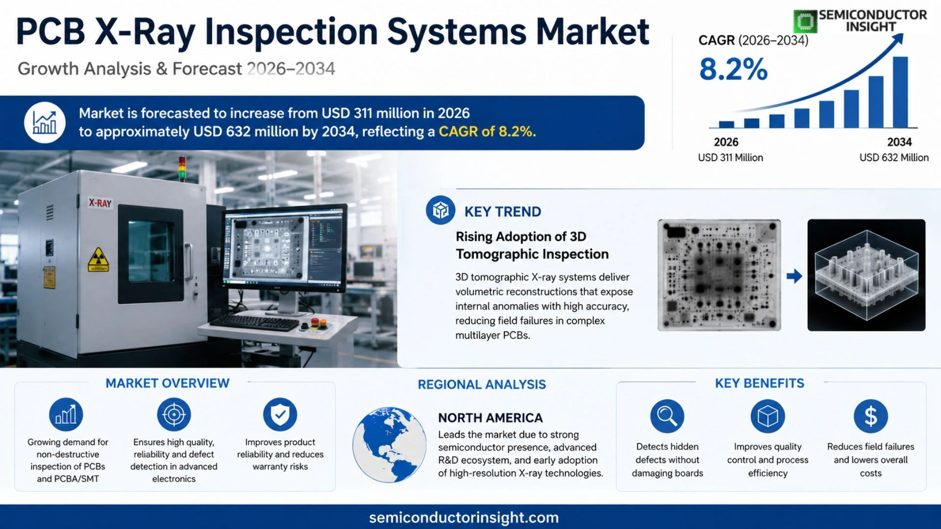
PCB X-Ray Inspection Systems market is forecasted to increase from USD 311 million in 2026 to approximately USD 632 million by 2034, reflecting a compound annual growth rate of about 8.2 % over the period.
PCB X‑Ray Inspection Systems are non‑destructive inspection solutions used for printed circuit boards (PCBs) and assembled boards (PCBA/SMT). A typical system combines a micro‑focus or high‑power X‑ray source, high‑resolution detectors, precision motion hardware and shielding, together with reconstruction and automated defect‑recognition software that delivers volumetric “inside‑the‑product” evidence without damaging the sample.
MARKET DRIVERS
Increasing Complexity of Multi‑Layer PCBs
The surge in high‑density interconnect (HDI) designs forces manufacturers to adopt non‑contact inspection methods. X‑ray systems can penetrate dense copper stacks, revealing hidden voids and micro‑cracks that optical tools miss. As board layer counts climb from eight to twelve in advanced telecommunications equipment, the need for reliable X‑ray verification becomes a decisive factor in production yield.
Regulatory and Reliability Demands
Automotive safety standards such as ISO 26262 and aerospace mandates like DO‑160 require demonstrable defect‑free assemblies. Compliance audits increasingly request X‑ray imagery as proof of solder joint integrity. Companies that embed this capability into their line‑side testing not only avoid costly re‑work but also enhance their credibility with OEMs.
➤ “Strategic investment in X‑ray inspection translates directly into lower field failure rates and stronger supplier relationships.”
Collectively, these forces elevate the PCB X-Ray Inspection Systems Market by pushing adoption beyond niche applications toward mainstream manufacturing lines, reshaping capital budgeting priorities across the sector.
MARKET CHALLENGES
Cost Sensitivity in High‑Volume Production
Deploying a full‑feature X‑ray station often exceeds six figures, a hurdle for contract manufacturers operating thin margins. While the long‑term ROI becomes evident after defect‑related scrap declines, the initial cash outlay can delay technology rollout, especially in regions where financing options remain limited.
Other Challenges
Supply Chain Constraints
The specialized detector modules and high‑precision X‑ray tubes rely on a narrow supplier base. Recent component shortages have extended lead times to twelve months, compelling buyers to stock safety inventory or explore refurbished alternatives, both of which add complexity to project planning.
MARKET RESTRAINTS
Limited Skilled Personnel
Operating and interpreting high‑resolution X‑ray images demands a blend of engineering expertise and radiological safety knowledge. The talent pool capable of calibrating exposure parameters, managing shielding protocols, and diagnosing subtle defect signatures remains small, creating a bottleneck that slows broader deployment despite clear technical advantages.
MARKET OPPORTUNITIES
AI‑Assisted Defect Classification
Machine‑learning algorithms trained on thousands of annotated X‑ray images are beginning to flag out‑of‑spec features with near‑human accuracy. Integration of AI modules into inspection platforms promises faster throughput and predictive maintenance insights, opening a revenue stream for vendors willing to license cloud‑based analytics services.
PCB X-Ray Inspection Systems Market Trends
Rising Adoption of 3D Tomographic Inspection
In high‑density multilayer boards, concealed defects such as micro‑via voids or hidden solder cracks have become a primary source of field failures. 3D tomographic X‑ray systems now deliver volumetric reconstructions that expose these internal anomalies with sub‑millimeter accuracy. Manufacturers adopting this capability report yield improvements of 4‑6 % on average, because early detection allows process engineers to adjust plating and reflow parameters before large‑scale production. The shift toward 3D inspection is driven by the need to meet the reliability expectations of AI‑server and automotive electronics customers, where a single defective joint can trigger costly warranty claims.
Other Trends
AI‑Enhanced Defect Recognition
Algorithmic advances have turned raw X‑ray imagery into actionable quality metrics. By training neural networks on labeled defect libraries, leading vendors now achieve false‑call rates below 2 %, compared with legacy rule‑based systems that hovered around 8 %. This reduction in noise accelerates automated disposition, enabling manufacturers to feed defect statistics directly into MES dashboards for root‑cause analysis. Consequently, inspection stations are transitioning from a sampling role to a continuous monitoring function that supports closed‑loop yield optimization.
Supply‑Chain Consolidation of Core Components
Stability of X‑ray tubes, high‑resolution detectors, and precision motion platforms has emerged as a strategic bottleneck. OEMs that have secured long‑term contracts with tube manufacturers report gross margins edging toward the upper 50 % range, reflecting lower component cost volatility. At the same time, firms investing in in‑house detector refurbishment capabilities reduce total cost of ownership and improve service turnaround, which is increasingly important as customers demand higher throughput on larger‑format boards.
COMPETITIVE LANDSCAPE
Key Industry Players
PCB X‑Ray Inspection Systems – Competitive Overview
The dominance of a few platform‑focused firms defines the current structure of the PCB X‑Ray Inspection market. ViTrox leads with a modular architecture that couples a stable micro‑focus tube, high‑resolution flat‑panel detector, and adaptable motion mechanics. This configuration permits rapid re‑engineering for larger boards or higher throughput, giving ViTrox a decisive edge in both high‑volume automotive and data‑center segments. Its ability to bundle software licensing, AI‑enhanced defect classification, and long‑term service contracts translates into gross margins that exceed the industry median, reinforcing its position as the benchmark for platform evolution.
Beyond the flagship vendors, a cluster of specialized manufacturers sustains market depth. Viscom offers compact inline solutions optimized for SMT lines, while Nordson targets the high‑throughput niche with rugged tube designs. Omron’s emphasis on precision motion complements its broader automation portfolio. Nikon and ZEISS contribute premium imaging optics that improve defect detectability on multilayer HDI boards. Waygate Technologies (Baker Hughes) leverages deep‑well X‑ray tubes for aerospace applications, and Comet Yxlon provides cost‑effective offshore units for emerging markets. Test Research Inc., Seamark ZM, Zhengye Technology, Saki Corporation, XAVIS Co., SEC, Techvalley, Goepel Electronic, Scienscope, SXRAY, and Creative Electron round out the ecosystem, each carving out niches ranging from prototype‑scale inspection to low‑dose tomographic systems. Their collective activity pushes technology boundaries, fuels competition on price and functionality, and ensures that end‑users have alternatives tailored to specific reliability targets.
List of Key PCB X‑Ray Inspection Systems Companies Profiled
- ViTrox
- Viscom
- Nordson
- Omron
- Nikon
- Waygate Technologies (Baker Hughes)
- Comet Yxlon
- Test Research Inc. (TRI)
- Seamark ZM
- Zhengye Technology
- ZEISS
- Saki Corporation
- XAVIS Co., Ltd.
- SEC
- Techvalley
- Goepel Electronic
- Scienscope
- SXRAY
- Creative Electron
Segment Analysis:
| Segment Category | Sub-Segments | Key Insights |
| By Type |
|
Inline X‑ray Inspection Equipment
|
| By Application |
|
Automotive Electronics
|
| By End User |
|
EMS/SMT Assemblers
|
| By Technology |
|
3D/Tomography Inspection
|
| By Production Line |
|
Large‑volume Production
|
Regional Analysis: PCB X-Ray Inspection Systems Market
Early‑stage pilots in silicon‑photonic fabs have accelerated migration to high‑energy X‑ray units capable of resolving sub‑micron voids. Vendors are integrating AI‑driven defect classification, reducing operator fatigue and sharpening root‑cause analysis for complex multilayer boards.
Federal safety directives increasingly mandate non‑destructive testing for critical defence and medical devices. These rules push assembly houses toward X‑ray inspection as a compliance checkpoint, reinforcing demand for certified equipment.
Aerospace and electric‑vehicle suppliers dominate the buyer profile, each requiring traceable defect documentation. Smaller contract manufacturers follow suit to meet their customers’ quality contracts, expanding the installed base beyond the tier‑one segment.
A handful of legacy equipment makers retain market share through extensive service networks, while new entrants differentiate with modular designs that allow retro‑fit upgrades, intensifying pressure on pricing and after‑sales support.
Europe
European manufacturers are responding to a tightening of quality standards in automotive safety systems, where hidden solder defects trigger costly recalls. The region benefits from a coordinated standards framework that encourages cross‑border technology sharing, allowing midsize PCB assemblers to pool resources and adopt X‑ray inspection without prohibitive capital outlay. Additionally, sustainability initiatives are urging producers to minimize waste, and X‑ray systems provide early defect detection that reduces scrap rates. These dynamics foster a steady growth trajectory for the PCB X‑Ray Inspection Systems Market across Germany, the Benelux, and Central Europe, with service contracts becoming a critical revenue source for equipment providers.
Asia‑Pacific
Asia‑Pacific’s expansion is driven by an explosive rollout of consumer electronics and a rapid up‑scaling of automotive electronics plants in China, Vietnam, and India. While cost considerations dominate purchasing decisions, the region’s manufacturers are increasingly aware of the long‑term expense of field failures, prompting a shift toward higher‑precision inspection. Local OEMs are also forging joint ventures with Western technology firms to acquire X‑ray capability, accelerating knowledge transfer. The combined effect is a nuanced market where low‑cost solutions coexist with premium systems tailored for high‑volume, high‑complexity board productions.
South America
In South America, the market’s evolution is tied to the gradual maturation of the region’s electronics assembly sector, particularly in Brazil and Argentina. Government incentives for advanced manufacturing have lowered barriers for adopting sophisticated inspection equipment. Nevertheless, limited access to skilled technicians means providers are bundling training and remote diagnostics with hardware sales, ensuring operational readiness. This service‑centric approach is shaping buyer expectations and nudging the market toward higher‑value, support‑intensive offerings.
Middle East & Africa
The Middle East & Africa region is witnessing nascent interest in PCB X‑ray inspection as aerospace and defence projects gain momentum, especially in the United Arab Emirates and Saudi Arabia. Investment in smart‑factory initiatives is prompting early adopters to prototype inspection lines that can validate complex multilayer designs. In Africa, a handful of electronics hubs are exploring outsourcing opportunities, and the ability to certify board integrity becomes a competitive differentiator. Consequently, the market is characterized by pilot deployments and a growing demand for turnkey solutions that include both hardware and ongoing expertise.
Report Scope
This market research report provides a comprehensive analysis of the PCB X-Ray Inspection Systems Market , covering the forecast period 2026–2034. It offers detailed insights into market dynamics, technological advancements, competitive landscape, and key trends shaping the industry.
Key focus areas of the report include:
- Market Overview: The report begins with an overview outlining its current market scenario, key growth indicators, and industry transformation drivers. It discusses macroeconomic factors, demand–supply balance, regulatory landscape, and the strategic role of semiconductors in powering advancements across industries such as automotive, telecommunications, consumer electronics, and industrial automation.
- Market Size & Forecast: Historical data and future projections for revenue, unit shipments, and market value across major regions and segments.
- Segmentation Analysis: Detailed breakdown by product type, technology, application, and end-user industry to identify high-growth segments and investment opportunities.
- Regional Insights: Insights into market performance across North America, Europe, Asia-Pacific, Latin America, and the Middle East & Africa, including country-level analysis where relevant.
- Competitive Landscape: Profiles of leading market participants, including their product offerings, R&D focus, manufacturing capacity, pricing strategies, and recent developments such as mergers, acquisitions, and partnerships.
- Technology Trends & Innovation: Assessment of emerging technologies, integration of AI/IoT, semiconductor design trends, fabrication techniques, and evolving industry standards.
- Market Drivers & Restraints: Evaluation of factors driving market growth along with challenges, supply chain constraints, regulatory issues, and market-entry barriers.
- Stakeholder Insights: Insights for component suppliers, OEMs, system integrators, investors, and policymakers regarding the evolving ecosystem and strategic opportunities.
Primary and secondary research methods are employed, including interviews with industry experts, data from verified sources, and real-time market intelligence to ensure the accuracy and reliability of the insights presented.
FREQUENTLY ASKED QUESTIONS:
What is the current market size of PCB X-Ray Inspection Systems Market?
-> PCB X-Ray Inspection Systems Market was valued at USD 311 million in 2025 and is expected to reach USD 573 million by 2034 at a CAGR of 8.2% during the forecast period.
Which key companies operate in PCB X-Ray Inspection Systems Market?
-> Key players include ViTrox, Viscom, Nordson, Omron, Unicomp Technology, NIKON, Waygate Technologies (Baker Hughes), Comet Yxlon, Test Research Inc. (TRI), Seamark ZM, Zhengye Technology, ZEISS, Saki Corporation, XAVIS Co., Ltd., SEC, Techvalley, Goepel Electronic, Scienscope, SXRAY, Creative Electron.
What are the key growth drivers?
-> Key growth drivers include AI‑driven demand for higher‑layer count HDI and substrate PCBs, rising need for hidden‑defect detection in AI servers, high‑speed networking and automotive electronics, and broader adoption of non‑destructive X‑ray inspection for quality assurance.
Which region dominates the market?
-> Asia dominates the PCB X‑Ray Inspection Systems market, driven by strong manufacturing bases in China, Japan, and South Korea and increasing demand from electronics, data‑center and automotive sectors.
What are the emerging trends?
-> Emerging trends include development of large‑format and 3D/tomographic X‑ray systems, low‑dose imaging, AI/ML‑enabled defect classification, and integration of inspection data with MES/quality platforms for closed‑loop yield improvement.

Get Sample Report PDF for Exclusive Insights
Report Sample Includes
- Table of Contents
- List of Tables & Figures
- Charts, Research Methodology, and more...
 Download Sample Report PDF