Market Insights
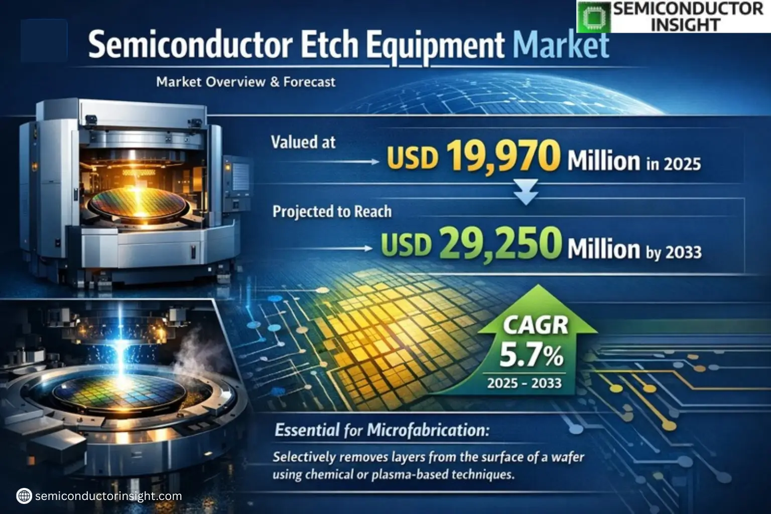
Global Semiconductor Etch Equipment Market was valued at USD 19,970 million in 2025 and is projected to reach USD 29,250 million by 2033, exhibiting a CAGR of 5.7% during the forecast period.
Semiconductor Etch Equipment is critical in microfabrication processes, where it selectively removes layers from the surface of a wafer using chemical or plasma-based techniques. This equipment shapes thin films into precise patterns essential for semiconductor device manufacturing. The process involves dry etching (plasma-based) and wet etching (chemical solutions), with dry etching dominating the market due to its higher precision and compatibility with advanced node technologies.
The market growth is driven by increasing demand for miniaturized electronic components, advancements in semiconductor fabrication technologies, and rising investments in foundries. Key players such as Lam Research, TEL, and Applied Materials collectively hold approximately 90% of the market share. Dry etch equipment accounts for 89% of the market, while logic and memory applications represent nearly 80% of demand. Emerging trends include the adoption of atomic layer etching (ALE) for next-generation chips and expansion in Asia-Pacific semiconductor hubs.
MARKET DRIVERS
Increasing Demand for Advanced Semiconductor Devices
Semiconductor Etch Equipment Market is experiencing significant growth due to rising demand for high-performance chips in AI, 5G, and IoT applications. Major foundries are investing heavily in cutting-edge nodes below 7nm, requiring sophisticated dry etching solutions. Global wafer fab equipment spending is projected to exceed USD 100 billion annually, with etch systems representing approximately 15% of this expenditure.
Technology Miniaturization Trends
As semiconductor geometries shrink below 5nm, atomic-level precision in etching becomes critical. Leading manufacturers are adopting advanced plasma etching techniques to achieve sub-10nm feature sizes. The transition to 3D NAND and GAAFET architectures is particularly driving demand for selective etching solutions with superior aspect ratio capabilities.
Additionally, the shift towards EUV lithography is creating complementary demand for ultra-precise etch systems that can handle complex multi-patterning requirements.
MARKET CHALLENGES
Technical Complexities in Advanced Node Processing
Developing etch solutions for sub-5nm nodes presents substantial technical hurdles, including control of plasma-induced damage and critical dimension uniformity. Semiconductor Etch Equipment Market faces increasing R&D costs, with leading manufacturers spending over USD 1 billion annually on process development.
Other Challenges
Supply Chain Constraints
Global semiconductor shortage has highlighted vulnerabilities in the equipment supply chain, with lead times for critical components extending beyond 12 months. This is particularly acute for precision parts used in plasma etch chambers.
MARKET RESTRAINTS
High Capital Investment Requirements
Semiconductor Etch Equipment Market faces growth limitations due to the substantial capital expenditure required for new fabrication facilities. A state-of-the-art 300mm wafer fab can cost upwards of USD 20 billion, with etch tools representing a significant portion of this investment.
MARKET OPPORTUNITIES
Expansion in Emerging Applications
Semiconductor Etch Equipment Market is poised for growth through emerging applications such as power semiconductors for electric vehicles and RF devices for 6G networks. The GaN and SiC device markets are expected to grow at 15% CAGR, creating new demand for specialized etching solutions.
Semiconductor Etch Equipment Market Trends
Rapid Market Growth Driven by Semiconductor Demand
Global Semiconductor Etch Equipment Market is experiencing steady growth, valued at USD 19.97 billion in 2025 and projected to reach USD 29.25 billion by 2033 at a 5.7% CAGR. This expansion is fueled by increasing demand for advanced logic and memory chips, particularly for AI, 5G, and IoT applications. Semiconductor etching remains a critical step in chip manufacturing, with dry etching dominating 89% of the market due to its precision in advanced node manufacturing.
Other Trends
Market Consolidation Among Equipment Vendors
The semiconductor etch equipment industry shows high market concentration, with Lam Research, TEL, and Applied Materials collectively controlling approximately 90% market share. This oligopoly results from the significant R&D investments and technological barriers required to develop next-generation etching solutions.
Regional Production Shifts and Supply Chain Dynamics
Asia-Pacific dominates semiconductor etch equipment consumption with over 80% market share, led by China, Taiwan, South Korea, and Japan. Recent government initiatives like the U.S. CHIPS Act and EU Chips Act are driving capacity expansion in other regions. The equipment market faces challenges from geopolitical factors affecting supply chains and technology transfers between regions.
Technology Evolution in Etching Processes
Equipment manufacturers are developing advanced solutions for sub-5nm node production, with increasing focus on atomic layer etching (ALE) and selective etching technologies. The transition to new materials like high-k dielectrics and new transistor architectures requires continuous innovation in etching processes and equipment.
Application-Specific Equipment Demand
Logic and memory applications account for 80% of semiconductor etch equipment usage, with particular growth in 3D NAND and DRAM manufacturing. The power device and MEMS segments are also driving demand for specialized etching solutions as these technologies gain importance in automotive and industrial applications.
COMPETITIVE LANDSCAPE
Key Industry Players
Oligopolistic Market Dominated by Top Equipment Manufacturers
Semiconductor Etch Equipment Market is highly concentrated, with Lam Research, Tokyo Electron Limited (TEL), and Applied Materials collectively controlling approximately 90% of global market share. These three players dominate both dry and wet etch equipment segments through continuous R&D investments and strategic partnerships with leading foundries. Lam Research maintains technological leadership in plasma etch systems, while TEL has strong presence in dielectric etch applications. Applied Materials complements its etch portfolio with integrated deposition-etch solutions for advanced nodes.
Niche players like Hitachi High-Tech and AMEC focus on specialized applications such as MEMS and compound semiconductor etching. Emerging Chinese manufacturers including NAURA are gaining traction in domestic markets through government-supported semiconductor self-sufficiency initiatives. Equipment suppliers continue to develop atomic layer precision etching solutions for sub-3nm nodes, with significant competition around high-aspect-ratio etching capabilities for 3D NAND and DRAM applications.
List of Key Semiconductor Etch Equipment Companies Profiled
- Lam Research Corporation
- Tokyo Electron Limited (TEL)
- Applied Materials, Inc.
- Hitachi High-Tech Corporation
- Oxford Instruments plc
- SPTS Technologies (KLA Corporation)
- Plasma-Therm LLC
- GigaLane Co., Ltd.
- SAMCO Inc.
- Advanced Micro-Fabrication Equipment Inc. (AMEC)
- NAURA Technology Group Co., Ltd.
- Ultratech (Veeco Instruments Inc.)
- Canon Anelva Corporation
- Eugenus Inc.
- Singulus Technologies AG
Segment Analysis:
| Segment Category | Sub-Segments | Key Insights |
| By Type |
|
Dry Etch Equipment dominates the market due to:
|
| By Application |
|
Logic and Memory segment shows strongest demand because:
|
| By End User |
|
Foundries represent the largest consumer segment because:
|
| By Technology Node |
|
5nm and below segment is experiencing fastest growth due to:
|
| By Chamber Configuration |
|
Multi-Chamber configuration is gaining prominence because:
|
Regional Analysis: Global Semiconductor Etch Equipment Market
Taiwan accounts for over 60% of global foundry capacity, with TSMC driving continuous upgrades in etch equipment technology for advanced nodes. The concentration of tier-1 foundries creates a high-value market for precision etch systems.
Samsung and SK Hynix require specialized etch solutions for 3D NAND and DRAM production. The country’s strength in memory semiconductors creates unique demand for high-aspect ratio etching capabilities.
Despite US restrictions, Chinese foundries are accelerating domestic etch equipment adoption. SMIC and Yangtze Memory are working with local suppliers to develop alternative etch solutions amid technology access challenges.
Japanese firms like Tokyo Electron dominate certain etch equipment segments with superior materials science capabilities. Their technologies are critical for advanced packaging and specialty semiconductor production.
North America
North America remains a key innovation hub for semiconductor etch equipment, with major R&D centers developing next-generation etching technologies. The US benefits from leading equipment vendors like Applied Materials and Lam Research headquartered in Silicon Valley. Intel’s IDM 2.0 strategy is driving etch equipment upgrades across its fabs. The region sees strong demand from both logic and memory chip producers, with particular emphasis on GAAFET-compatible etching solutions. Government initiatives like the CHIPS Act are expected to boost domestic semiconductor production and related equipment demand.
Europe
Europe maintains strengths in specialty semiconductor applications requiring advanced etch solutions. ASML’s EUV leadership creates complementary demand for precision etching equipment. The region has notable capabilities in power semiconductors and MEMS production. Imec’s research partnerships with equipment makers drive etch technology innovation. Recent EU chip act provisions aim to strengthen the regional semiconductor supply chain. Automotive and industrial applications dominate etch equipment demand patterns in European fabs.
Middle East & Africa
The Middle East is emerging as a new growth area for semiconductor investments, particularly in Israel’s thriving fabless ecosystem and the UAE’s technology diversification efforts. While current etch equipment demand is modest, planned semiconductor projects could create new opportunities. South Africa has niche capabilities in compound semiconductor production requiring specialized etch solutions. The region benefits from growing partnerships with Asian and Western semiconductor firms.
South America
South America’s semiconductor etch equipment market remains underdeveloped but shows potential in Brazil’s established electronics manufacturing base. Argentina and Chile have nascent semiconductor research initiatives that may drive future equipment demand. The region primarily imports etch systems from global suppliers for limited domestic production needs. Growing interest in local electronics manufacturing could gradually increase equipment requirements.
Report Scope
This market research report provides a comprehensive analysis of the Semiconductor Etch Equipment Market, covering the forecast period 2025–2033. It offers detailed insights into market dynamics, technological advancements, competitive landscape, and key trends shaping the industry.
Key focus areas of the report include:
- Market Overview: The report begins with an overview outlining its current market scenario, key growth indicators, and industry transformation drivers. It discusses macroeconomic factors, demand–supply balance, regulatory landscape, and the strategic role of semiconductors in powering advancements across industries such as automotive, telecommunications, consumer electronics, and industrial automation.
- Market Size & Forecast: Historical data and future projections for revenue, unit shipments, and market value across major regions and segments.
- Segmentation Analysis: Detailed breakdown by product type, technology, application, and end-user industry to identify high-growth segments and investment opportunities.
- Regional Insights: Insights into market performance across North America, Europe, Asia-Pacific, Latin America, and the Middle East & Africa, including country-level analysis where relevant.
- Competitive Landscape: Profiles of leading market participants, including their product offerings, R&D focus, manufacturing capacity, pricing strategies, and recent developments such as mergers, acquisitions, and partnerships.
- Technology Trends & Innovation: Assessment of emerging technologies, integration of AI/IoT, semiconductor design trends, fabrication techniques, and evolving industry standards.
- Market Drivers & Restraints: Evaluation of factors driving market growth along with challenges, supply chain constraints, regulatory issues, and market-entry barriers.
- Stakeholder Insights: Insights for component suppliers, OEMs, system integrators, investors, and policymakers regarding the evolving ecosystem and strategic opportunities.
Primary and secondary research methods are employed, including interviews with industry experts, data from verified sources, and real-time market intelligence to ensure the accuracy and reliability of the insights presented.
FREQUENTLY ASKED QUESTIONS:
What is the current market size of Semiconductor Etch Equipment Market?
-> Semiconductor Etch Equipment Market was valued at USD 19,970 million in 2025 and is projected to reach USD 29,250 million by 2033, exhibiting a CAGR of 5.7% during the forecast period.
Which key companies operate in Semiconductor Etch Equipment Market?
-> Key players include Lam Research, TEL, Applied Materials, Hitachi High-Tech, AMEC, Oxford Instruments, SPTS Technologies, Plasma-Therm, GigaLane, SAMCO, and NAURA, among others. The top three players account for approximately 90% of the total market.
What are the key growth drivers?
-> Key growth drivers include increasing demand for advanced semiconductor fabrication, technological advancements in etching processes, and rising investments in semiconductor manufacturing facilities.
Which region dominates the market?
-> Asia is the dominant region, with major contributions from China, Japan, and South Korea, driven by robust semiconductor manufacturing activities.
What are the emerging trends?
-> Emerging trends include adoption of dry etching technology (89% market share), expansion in logic and memory applications (80% share), and advancements in AI/IoT-driven semiconductor manufacturing.

Get Sample Report PDF for Exclusive Insights
Report Sample Includes
- Table of Contents
- List of Tables & Figures
- Charts, Research Methodology, and more...


