Market Insights
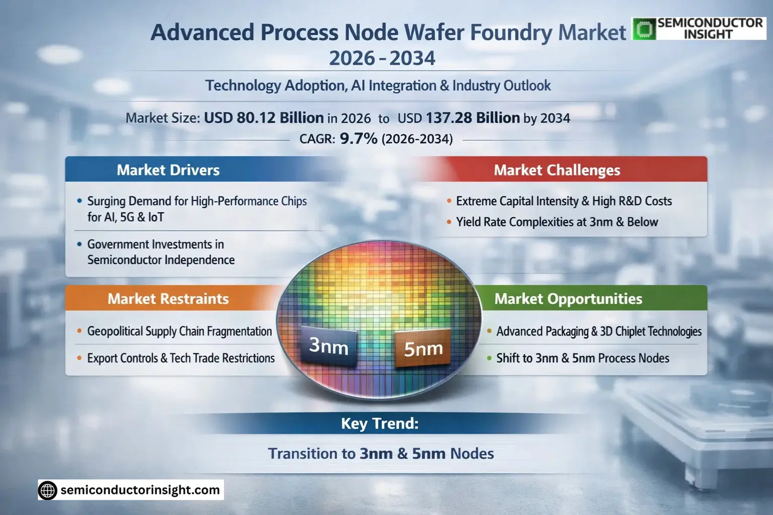
Global Advanced Process Node Wafer Foundry Market size was valued at USD 73.08 billion in 2025. The market is projected to grow from USD 80.12 billion in 2026 to USD 137.28 billion by 2034, exhibiting a CAGR of 9.7% during the forecast period.
Advanced process node wafer foundries specialize in manufacturing semiconductor wafers using cutting-edge fabrication technologies, typically ranging from 3nm to 20nm nodes. These facilities enable the production of high-performance chips for applications such as artificial intelligence, 5G networks, and autonomous vehicles by leveraging extreme ultraviolet (EUV) lithography and other precision techniques.
The market growth is driven by escalating demand for advanced computing solutions and the proliferation of IoT devices, though it faces challenges from rising R&D costs and geopolitical tensions affecting semiconductor supply chains. Leading foundries like TSMC and Samsung are accelerating their investments in next-generation nodes, with TSMC’s Arizona fab expansion representing a strategic move to strengthen North American production capabilities.
MARKET DRIVERS
Increasing Demand for High-Performance Chips
Advanced Process Node Wafer Foundry Market is driven by the growing need for high-performance semiconductors in 5G, AI, and IoT applications. Leading-edge nodes (5nm and below) enable faster processing with lower power consumption, making them essential for next-gen technologies. Foundries investing in advanced nodes are capturing significant market share as demand outpaces supply.
Government Investments in Semiconductor Independence
Nations worldwide are prioritizing domestic semiconductor capabilities through initiatives like the CHIPS Act, allocating over USD 52 billion to boost advanced manufacturing. This strategic push is accelerating capacity expansion in the Advanced Process Node Wafer Foundry Market, with TSMC, Samsung, and Intel leading the node race.
Transition to EUV lithography has enabled more cost-effective production at 7nm and below, with TSMC’s 3nm process achieving 70% yield rates, driving higher adoption.
MARKET CHALLENGES
Extreme Capital Intensity and R&D Costs
Building a new advanced node foundry requires USD 20+ billion investments, with EUV lithography tools costing up to USD 150 million per unit. Only three companies currently possess the financial resources to compete in the Advanced Process Node Wafer Foundry Market at 5nm and below.
Other Challenges
Yield Rate Complexities
Achieving >80% yields at 3nm requires overcoming quantum tunneling effects and thermal dissipation issues, adding months to process qualification timelines.
MARKET RESTRAINTS
Geopolitical Supply Chain Fragmentation
Export controls on advanced semiconductor equipment are creating bifurcated supply chains, with China developing indigenous 14nm capabilities while Western markets advance to 2nm. This division may temporarily slow the Advanced Process Node Wafer Foundry Market’s global growth trajectory.
MARKET OPPORTUNITIES
Advanced Packaging Technologies
Chiplet architectures and 3D stacking allow foundries to extend the value of mature nodes while incorporating advanced node components. This hybrid approach presents a USD 15 billion opportunity in the Advanced Process Node Wafer Foundry Market by 2027, with TSMC’s CoWoS platform leading adoption.
Advanced Process Node Wafer Foundry Market Trends
Transition to 3nm and 5nm Nodes Accelerates
Advanced Process Node Wafer Foundry Market is witnessing rapid adoption of 3nm and 5nm process technologies, driven by demand from smartphone and high-performance computing applications. Leading foundries like TSMC and Samsung are ramping up production capacities to meet growing requirements for these advanced nodes, which offer significant improvements in power efficiency and transistor density.
Other Trends
Geographic Expansion of Production Facilities
Major players are establishing new advanced node foundries in multiple regions to mitigate supply chain risks and meet local demand. The U.S. and China are emerging as key growth markets, with significant investments in domestic semiconductor manufacturing capabilities for advanced process nodes.
Diversification of Application Segments
While smartphones remain the dominant application, Advanced Process Node Wafer Foundry Market is seeing growing adoption in automotive electronics and AI processors. This diversification is driving demand for specialized node technologies optimized for different performance and power requirements across industries.
Technological Collaboration Intensifies
Foundries are increasingly partnering with design firms and end-users to co-develop customized process technologies. This trend is particularly evident in the HPC segment, where performance optimization at advanced nodes requires close collaboration throughout the development cycle.
Concentration of Market Share Among Top Players
Advanced Process Node Wafer Foundry Market remains highly concentrated, with TSMC, Samsung, and Intel Foundry Services accounting for the majority of global capacity in cutting-edge nodes below 7nm. This consolidation presents both opportunities and challenges for fabless semiconductor companies.
COMPETITIVE LANDSCAPE
Key Industry Players
Semiconductor Giants Dominate Advanced Node Foundry Market
Taiwan Semiconductor Manufacturing Company (TSMC) leads the Advanced Process Node Wafer Foundry Market with over 55% global share in 2025, maintaining technological leadership through rapid node transitions and massive R&D investments. The market structure remains highly concentrated with TSMC and Samsung Foundry collectively controlling nearly 80% of sub-10nm production capacity, creating significant barriers to entry for competitors.
Emerging Chinese foundries are gaining traction in mature advanced nodes (14nm-28nm) through government subsidies, while specialty foundries like GlobalFoundries focus on differentiated technologies. Intel’s re-entry via IFS demonstrates the strategic importance of advanced nodes, though volume production remains limited compared to Asian leaders.
List of Key Advanced Process Node Wafer Foundry Companies Profiled
- Taiwan Semiconductor Manufacturing Company (TSMC)
- Samsung Foundry
- Intel Foundry Services (IFS)
- GlobalFoundries
- Semiconductor Manufacturing International Corporation (SMIC)
- Huahong Grace Semiconductor Manufacturing Corporation (HLMC)
- United Microelectronics Corporation (UMC)
- Powerchip Semiconductor Manufacturing Corporation
- Tower Semiconductor
- Vanguard International Semiconductor Corporation
- Dongbu HiTek
- MagnaChip Semiconductor
- Skyworks Solutions
- VisIC Technologies
- X-FAB Silicon Foundries
Segment Analysis:
| Segment Category | Sub-Segments | Key Insights |
| By Type |
|
5nm Process Node currently dominates as the most balanced solution between performance and cost efficiency.
|
| By Application |
|
Smartphones remain the primary growth driver for advanced node adoption.
|
| By End User |
|
Fabless Semiconductor Companies account for majority of advanced node demand.
|
| By Technology Complexity |
|
Chiplet-Based Designs are gaining significant traction in advanced nodes.
|
| By Design Approach |
|
Platform-Based Designs are becoming increasingly important for advanced nodes.
|
Regional Analysis: Advanced Process Node Wafer Foundry Market
Asia-Pacific leads in sub-7nm process adoption with TSMC’s volume production of 3nm wafers. Foundries are pioneering gate-all-around transistor architectures while European and American counterparts still perfect FinFET technologies.
Proximity to semiconductor materials suppliers and equipment manufacturers enables faster iteration cycles. Regional clustering of ecosystem partners reduces time-to-market for new process node developments.
Foundries are implementing AI-driven predictive maintenance and defect detection systems. Machine learning models optimize lithography patterns and deposition processes, improving yields at advanced nodes.
Over 15 new advanced node fab projects are underway across Taiwan, South Korea, and China. These facilities will collectively add >1 million wafers/month of <7nm capacity by 2026.
North America
The North American Advanced Process Node Wafer Foundry Market is driven by strong demand from AI accelerator and HPC chip designers. Intel’s renewed foundry strategy focuses on catching up in EUV-based processes while leveraging packaging innovations. Regional advantages include proximity to fabless semiconductor companies and DOE-funded research in next-generation nanomaterials. However, the region faces challenges in matching Asia’s cost structures and skilled workforce availability for high-volume production.
Europe
Europe maintains niche strengths in specialty semiconductor processes and collaborates closely with equipment manufacturers like ASML. The EU Chips Act is stimulating investments in advanced node R&D, particularly in Germany and France. While lacking leading-edge volume production, European foundries excel in embedded non-volatile memory and power-efficient process variants for automotive applications.
Middle East & Africa
Emerging as a dark horse, the Middle East is making strategic investments in semiconductor manufacturing capabilities. Saudi Arabia’s Vision 2030 includes plans for advanced packaging and testing facilities. The region benefits from abundant energy resources crucial for power-intensive wafer fabs, though technology transfer remains challenging.
South America
South America shows growing interest in semiconductor self-sufficiency, particularly for industrial and defense applications. Brazil’s CEITEC focuses on specialized node development, while regional collaborations aim to build foundational expertise. The market remains in early stages for advanced nodes but shows long-term potential.
Report Scope
This market research report provides a comprehensive analysis of the Advanced Process Node Wafer Foundry Market, covering the forecast period 2025–2034. It offers detailed insights into market dynamics, technological advancements, competitive landscape, and key trends shaping the industry.
Key focus areas of the report include:
- Market Overview: The report begins with an overview outlining its current market scenario, key growth indicators, and industry transformation drivers. It discusses macroeconomic factors, demand–supply balance, regulatory landscape, and the strategic role of semiconductors in powering advancements across industries such as automotive, telecommunications, consumer electronics, and industrial automation.
- Market Size & Forecast: Historical data and future projections for revenue, unit shipments, and market value across major regions and segments.
- Segmentation Analysis: Detailed breakdown by product type, technology, application, and end-user industry to identify high-growth segments and investment opportunities.
- Regional Insights: Insights into market performance across North America, Europe, Asia-Pacific, Latin America, and the Middle East & Africa, including country-level analysis where relevant.
- Competitive Landscape: Profiles of leading market participants, including their product offerings, R&D focus, manufacturing capacity, pricing strategies, and recent developments such as mergers, acquisitions, and partnerships.
- Technology Trends & Innovation: Assessment of emerging technologies, integration of AI/IoT, semiconductor design trends, fabrication techniques, and evolving industry standards.
- Market Drivers & Restraints: Evaluation of factors driving market growth along with challenges, supply chain constraints, regulatory issues, and market-entry barriers.
- Stakeholder Insights: Insights for component suppliers, OEMs, system integrators, investors, and policymakers regarding the evolving ecosystem and strategic opportunities.
Primary and secondary research methods are employed, including interviews with industry experts, data from verified sources, and real-time market intelligence to ensure the accuracy and reliability of the insights presented.
FREQUENTLY ASKED QUESTIONS:
What is the current market size of Advanced Process Node Wafer Foundry Market?
-> Advanced Process Node Wafer Foundry Market size was valued at USD 73.08 billion in 2025. The market is projected to grow from USD 80.12 billion in 2026 to USD 137.28 billion by 2034, exhibiting a CAGR of 9.7% during the forecast period.
Which key companies operate in Advanced Process Node Wafer Foundry Market?
-> Key players include TSMC, Samsung Foundry, Intel Foundry Services (IFS), GlobalFoundries, SMIC, and HLMC, among others.
What are the key application segments?
-> Key applications include High Performance Computing (HPC), smartphone, network communication, consumer electronics, and automotive electronics.
What are the major process node segments?
-> Major segments include 3nm, 5nm, 7nm, and grouped 10/12/14/16/20nm technologies.
Which region dominates the market?
-> Asia holds the largest market share, with significant contributions from China, Japan, and South Korea.
Get Sample Report PDF for Exclusive Insights
Report Sample Includes
- Table of Contents
- List of Tables & Figures
- Charts, Research Methodology, and more...