Semiconductor Critical Dimension-Scanning Electron Microscopes (CD-SEM) Market Insights
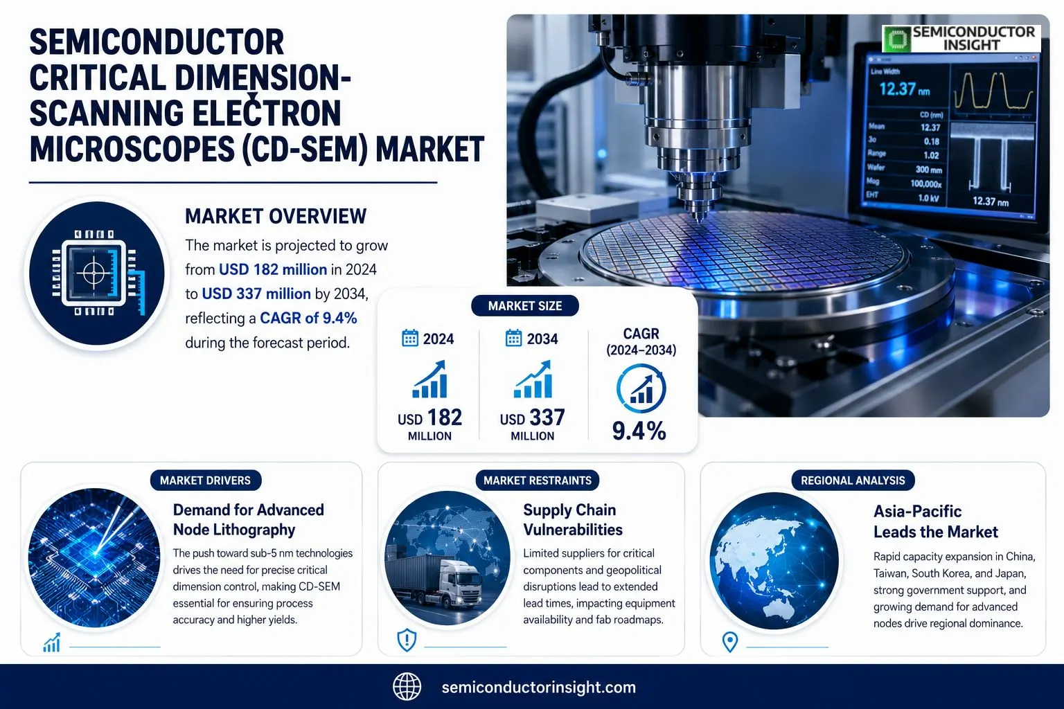
Semiconductor Critical Dimension-Scanning Electron Microscopes (CD‑SEM) market size was USD 182 million in 2024 and is expected to reach USD 337 million by 2034, reflecting a compound annual growth rate of roughly 9.4 %.
A Critical Dimension SEM (CD‑SEM) is a purpose‑built instrument that measures the width and profile of patterned features on semiconductor wafers. It provides line‑width control for logic, memory and advanced‑node production, allowing process engineers to verify compliance with increasingly stringent design rules.The upward trend stems from the push toward sub‑5 nm technologies, where tighter tolerances make CD‑SEM indispensable. Expansion of IoT devices and automotive electronics further fuels demand for high‑resolution metrology tools. Leading suppliers such as Hitachi, Advantest, Applied Materials and HOLON have announced new high‑resolution models and service programs aimed at shortening cycle time for fabs worldwide.
MARKET DRIVERS
Demand for Advanced Node Lithography
Manufacturers targeting sub‑10‑nm logic devices rely on tighter critical‑dimension control, and the Semiconductor Critical Dimension-Scanning Electron Microscopes (CD-SEM) Market supplies the precision needed to verify feature widths below 20 nm. As design rules shrink, process engineers turn to CD‑SEMs to detect pattern irregularities early, reducing costly re‑works on the fab floor.
Push for Higher Throughput and Accuracy
Recent instrument upgrades incorporate multi‑beam optics and faster scan rates, allowing fabs to examine more wafers per shift without sacrificing measurement fidelity. This efficiency gain translates directly into higher equipment utilization, a factor that many chipmakers cite as a primary justification for capital allocation to new CD‑SEMs.
➤ “The ability to resolve sub‑5 nm line‑edge roughness in real‑time has become a decisive advantage for leading foundries.”
Consequently, the accelerated adoption of these next‑generation tools is reshaping the competitive landscape, prompting equipment vendors to deepen their service portfolios and offering bundled analytics that further embed CD‑SEM data into process control loops.
MARKET CHALLENGES
Technical Complexity and Calibration
Maintaining nanometer‑level accuracy demands rigorous calibration protocols, and the expertise required to execute them is scarce. Facilities that lack dedicated metrology specialists often face longer downtime for instrument qualification, eroding the productivity gains promised by high‑speed CD‑SEMs.
Other Challenges
Cost Sensitivity
The upfront capital outlay for state‑of‑the‑art CD‑SEM systems remains steep, and many mid‑size fab operators must balance this expense against other pressing investments such as EUV lithography. Budget constraints can delay upgrades, creating a lag between technology roadmaps and measurement capability.
MARKET RESTRAINTS
Supply Chain Vulnerabilities
Critical components for CD‑SEMssuch as high‑purity electron sources and precision lensesare sourced from a limited pool of suppliers. Recent disruptions in raw‑material logistics have led to extended lead times, compelling some manufacturers to postpone equipment purchases despite clear process benefits.
MARKET OPPORTUNITIES
Emerging Applications in 3D Integration
Three‑dimensional stacking technologies, including heterogeneous integration and TSV (through‑silicon‑via) architectures, demand metrology that can access buried features without damaging the stack. Advanced CD‑SEM platforms equipped with variable‑pressure and low‑energy electron beams are uniquely positioned to meet this need, opening a new revenue stream for vendors willing to tailor solutions for 3D‑IC producers.
Semiconductor Critical Dimension-Scanning Electron Microscopes (CD-SEM) Market Trends
Shift Toward High‑Resolution CD‑SEM Systems
The adoption of sub‑5 nm logic processes is compelling equipment makers to prioritize resolution over throughput. Manufacturers are integrating advanced electron optics and detector arrays that can resolve line‑edge roughness at sub‑nanometer scales. This technical upgrade reduces the margin for error in pattern transfer, a factor that directly influences yield on high‑density wafers. As a result, fabs are allocating a larger share of capital expenditure to high‑resolution CD‑SEM units, even if the unit cost exceeds that of legacy instruments. The trend reflects a broader industry push for precision that outweighs the traditional emphasis on speed, reshaping the equipment purchasing hierarchy within the Semiconductor Critical Dimension-Scanning Electron Microscopes (CD-SEM) Market.
Other Trends
Emerging Demand from 3‑nm Logic Nodes
Design teams targeting the 3‑nm node are encountering tighter critical dimension windows, prompting a surge in metrology activity. The need to monitor gate‑pitch variations and fin height uniformity on both 4‑inch and 6‑inch wafers has led to an expansion of the application portfolio for CD‑SEM tools. Vendors are responding with modular software upgrades that enable real‑time feedback loops, allowing process engineers to correct deviations within a single production cycle. This capability shortens the time‑to‑market for new chip designs and mitigates the risk of costly re‑runs, thereby delivering a clear competitive advantage to fabs that invest early in these enhanced measurement solutions.
Regional Diversification of CD‑SEM Procurement
Historically, North America and Japan dominated equipment purchases, but recent fiscal reports show a marked increase in orders from East‑Asian foundries. The shift is driven by aggressive capacity expansion plans in China and South Korea, where manufacturers are scaling up 8‑inch and 12‑inch wafer lines to support AI‑centric workloads. Local governments are also offering incentives for advanced lithography infrastructure, nudging domestic players toward high‑performance CD‑SEM acquisitions. Meanwhile, European fabs are focusing on niche applications such as automotive power‑device production, where precision measurement adds regulatory value. This geographic redistribution creates a more balanced supply chain and presents opportunities for service providers to establish regional support hubs, enhancing after‑sales responsiveness and fostering tighter OEM‑customer relationships.
COMPETITIVE LANDSCAPE
Key Industry Players
Competitive Overview of CD‑SEM Suppliers
Hitachi High‑Technologies retains the largest share of the high‑resolution CD‑SEM segment, largely because its latest V‑Series instruments combine sub‑nanometer precision with a user‑friendly interface that satisfies the most demanding logic‑node fabs. Applied Materials leverages its broader metrology portfolio to cross‑sell CD‑SEM solutions to customers already using its deposition and etch equipment, creating a bundled value proposition that reinforces its market foothold. KLA Corporation, while known for defect inspection, has expanded aggressively into CD measurement with the e‑Line series, positioning itself as a one‑stop shop for yield‑critical metrology. These three firms together command more than half of the revenue, shaping pricing dynamics and influencing the direction of future technology roadmaps.Beyond the dominant trio, a cadre of specialist vendors sustains competitive pressure. Nanometrics supplies cost‑effective low‑resolution models that appeal to mid‑tier foundries seeking rapid cycle times. JEOL Ltd. and NIKON Metrology focus on ultra‑high‑resolution optics, differentiating through patented electron column designs that improve depth‑of‑focus. Oxford Instruments and Bruker target niche research laboratories with configurable platforms that can be retrofitted for emerging materials. Regional players such as Advantest (Japan), Hanyang (South Korea), and Taiwan Semiconductor Equipment Corp. (Taiwan) capture domestic market share by aligning product roadmaps with local fab upgrades. Their presence prevents excessive consolidation and encourages the larger incumbents to innovate on service, software integration, and after‑sales support.
List of Key Semiconductor Critical Dimension-Scanning Electron Microscopes Companies Profiled
- Hitachi High‑Technologies
- Applied Materials
- KLA Corporation
- Nanometrics
- JEOL Ltd.
- NIKON Metrology
- Oxford Instruments
- Bruker
- Advantest
- Hanyang Precision
- Taiwan Semiconductor Equipment Corp.
- Thermo Fisher Scientific
- Raith GmbH
- Carl Zeiss AG
- ASML (Metrology Division)
Segment Analysis:
| Segment Category | Sub-Segments | Key Insights |
| By Type |
|
High Resolution CD‑SEM drives innovation in advanced node manufacturing. • Enables precise measurement of sub‑10 nm features, supporting design shrinkage. • Preferred by leading fabs for its superior image fidelity and reduced defect risk. • Encourages ecosystem collaboration around tool optimization and software analytics. |
| By Application |
|
8‑Inch Wafer segment is pivotal for high‑volume logic and memory production. • Offers a balance of throughput and measurement accuracy for midsize fabs. • Aligns with the shift toward larger substrates to improve cost efficiency. • Fuels continuous improvements in stage stability and automation. |
| By End User |
|
Foundries shape the competitive landscape through early adoption of next‑generation CD‑SEM capabilities. • Prioritize instrument reliability to support high‑mix, high‑volume production cycles. • Collaborate closely with equipment vendors to co‑develop metrology workflows. • Emphasize training programs to maintain expertise across evolving process nodes. |
| By Resolution |
|
Sub‑10 nm Resolution is a strategic focus for leading fabs. • Enables verification of aggressive patterning techniques such as EUV and multi‑patterning. • Drives demand for enhanced electron optics and reduced noise designs. • Encourages software evolution toward AI‑assisted defect detection. |
| By Wafer Size |
|
300 mm Wafer adoption reflects the industry’s drive toward higher throughput. • Aligns with the migration to advanced nodes where larger substrates reduce per‑chip cost. • Fuels innovations in stage precision and vacuum stability. • Encourages ecosystem support for automation and data analytics integration. |
Regional Analysis: Semiconductor Critical Dimension-Scanning Electron Microscopes (CD-SEM) Market
North America
Major chipmakers allocate a sizable portion of their capital to research parks in Silicon Valley, where CD‑SEM performance is a decisive factor for transistor scaling. This investment fuels a steady pipeline of specification upgrades that vendors must anticipate.
Recent mergers among metrology service firms have tightened the supply chain, enabling tighter pricing structures while preserving service depth. Clients benefit from a single point of contact for maintenance and upgrade pathways.
Leading fabs prioritize CD‑SEMs with sub‑nanometer resolution for high‑volume logic nodes, whereas emerging manufacturers adopt mid‑range instruments to balance cost against yield improvement goals.
Federal initiatives targeting domestic semiconductor production have included subsidies earmarked for advanced metrology, indirectly boosting CD‑SEM procurement cycles.
Europe
European semiconductor hubs such as Dresden and Grenoble are integrating CD‑SEMs to support the continent’s shift toward advanced packaging. While the region lacks the sheer volume of North American fabs, it compensates with a strong focus on precision engineering and compliance with strict environmental standards. Collaborative projects funded by the EU increasingly require metrology data that meet a higher degree of traceability, prompting local vendors to offer customized calibration services. The resulting niche market encourages a blend of high‑end instrument sales and specialized consultancy, creating a resilient revenue stream for equipment manufacturers who can adapt to heterogeneous demand.
Asia‑Pacific
Asia‑Pacific’s rapid expansion of fabrication capacity, especially in Taiwan, South Korea, and China, translates into a growing appetite for CD‑SEMs capable of handling dense patterning. However, the region’s market is fragmented; tier‑1 foundries invest in the latest platforms, whereas smaller players rely on refurbished units to manage cost pressures. Government stimulus programs in several economies have accelerated procurement, yet export controls on certain technologies introduce uncertainty. Vendors that can navigate these regulatory nuances while offering flexible financing options are positioning themselves to capture a sizable share of the emerging demand curve.
South America
South America remains a peripheral player in the CD‑SEM arena, primarily because its semiconductor manufacturing base is modest. Nonetheless, a handful of research institutions in Brazil and Chile are establishing pilot lines that require high‑resolution imaging, generating niche demand for entry‑level systems. Partnerships with North American distributors help bridge the technology gap, and local governments are beginning to view advanced metrology as a strategic asset for future industrial diversification.
Middle East & Africa
The Middle East & Africa region shows limited direct consumption of CD‑SEMs, yet growing interest in semiconductor design services and test facilities is nudging the market forward. United Arab Emirates and South Africa host a few specialized labs that are beginning to source mid‑range instruments for research and low‑volume production. Procurement decisions are heavily influenced by the availability of skilled operators and after‑sales support, prompting equipment suppliers to explore joint‑venture service centers as a way to establish a foothold.
Report Scope
This market research report provides a comprehensive analysis of the Semiconductor Critical Dimension-Scanning Electron Microscopes (CD-SEM) Market , covering the forecast period 2026–2034. It offers detailed insights into market dynamics, technological advancements, competitive landscape, and key trends shaping the industry.
Key focus areas of the report include:
- Market Overview: The report begins with an overview outlining its current market scenario, key growth indicators, and industry transformation drivers. It discusses macroeconomic factors, demand–supply balance, regulatory landscape, and the strategic role of semiconductors in powering advancements across industries such as automotive, telecommunications, consumer electronics, and industrial automation.
- Market Size & Forecast: Historical data and future projections for revenue, unit shipments, and market value across major regions and segments.
- Segmentation Analysis: Detailed breakdown by product type, technology, application, and end-user industry to identify high-growth segments and investment opportunities.
- Regional Insights: Insights into market performance across North America, Europe, Asia-Pacific, Latin America, and the Middle East & Africa, including country-level analysis where relevant.
- Competitive Landscape: Profiles of leading market participants, including their product offerings, R&D focus, manufacturing capacity, pricing strategies, and recent developments such as mergers, acquisitions, and partnerships.
- Technology Trends & Innovation: Assessment of emerging technologies, integration of AI/IoT, semiconductor design trends, fabrication techniques, and evolving industry standards.
- Market Drivers & Restraints: Evaluation of factors driving market growth along with challenges, supply chain constraints, regulatory issues, and market-entry barriers.
- Stakeholder Insights: Insights for component suppliers, OEMs, system integrators, investors, and policymakers regarding the evolving ecosystem and strategic opportunities.
Primary and secondary research methods are employed, including interviews with industry experts, data from verified sources, and real-time market intelligence to ensure the accuracy and reliability of the insights presented.
FREQUENTLY ASKED QUESTIONS:
What is the current market size of Semiconductor Critical Dimension-Scanning Electron Microscopes (CD-SEM) Market?
-> Semiconductor Critical Dimension-Scanning Electron Microscopes (CD-SEM) Market was valued at USD 182 million in 2024 and is expected to reach USD 337 million by 2034.
What is the projected compound annual growth rate (CAGR) for the CD-SEM market?
-> The market is projected to grow at a CAGR of 9.4% during the forecast period.
Which key companies operate in Semiconductor Critical Dimension-Scanning Electron Microscopes (CD-SEM) Market?
-> Key players include Hitachi, Advantest, Applied Materials, and HOLON, among others.
What are the primary growth drivers for the CD-SEM market?
-> Growth is driven by the rising demand for advanced semiconductor manufacturing, increased adoption of IoT and AI‑driven devices, the need for higher‑resolution metrology, and continuous scaling of device geometries.
Which region dominates the CD-SEM market?
-> Asia‑Pacific leads the market, propelled by major semiconductor hubs in China, Japan, and South Korea.
What emerging trends are shaping the CD-SEM market?
-> Emerging trends include integration of AI for defect detection, development of ultra‑high‑resolution CD‑SEMs, and the shift toward 300 mm and larger wafer processing.
Get Sample Report PDF for Exclusive Insights
Report Sample Includes
- Table of Contents
- List of Tables & Figures
- Charts, Research Methodology, and more...
 Download Sample Report PDF