
Metrology (CD-SEM, OCD, X-ray) for Sub-3nm Market Insights
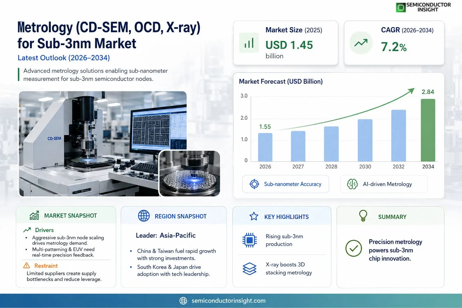
Global metrology (CD‑SEM, OCD, X‑ray) market size was valued at USD 1.45 billion in 2025. The market is projected to grow from USD 1.55 billion in 2026 to USD 2.84 billion by 2034, exhibiting a CAGR of 7.2% during the forecast period.
Critical dimension scanning electron microscopy (CD‑SEM), optical critical dimension (OCD) tools, and X‑ray based metrology systems are essential for measuring feature sizes below three nanometers on advanced semiconductor wafers. These techniques provide sub‑nanometer accuracy, enabling manufacturers to verify pattern fidelity and overlay compliance as node dimensions shrink.The market is accelerating because leading foundries are ramping up production of sub‑3nm chips, driving demand for higher‑resolution inspection solutions. Furthermore, increased R&D spending on extreme ultraviolet (EUV) lithography and the push toward heterogeneous integration are compelling equipment vendors to innovate faster metrology platforms.
MARKET DRIVERS
Advanced Node Scaling Demand
Semiconductor manufacturers are aggressively pursuing sub‑3nm logic nodes, which requires sub‑nanometer dimensional control. Metrology solutions such as CD‑SEM, OCD, and X‑ray provide the resolution needed to verify critical dimensions (CD) and overlay accuracy, driving strong adoption across leading fabs.
Integration of Multi‑Patterning Techniques
Multi‑patterning and extreme ultraviolet (EUV) lithography intensify the need for real‑time, high‑precision feedback. CD‑SEM offers rapid line‑edge detection, while OCD delivers three‑dimensional overlay measurements essential for stacked patterns.
➤ Metrology precision directly correlates with wafer yield improvements, often adding 5‑10% incremental yield for sub‑3nm processes.
The convergence of AI‑based defect detection and automated data analytics further enhances the value proposition of X‑ray metrology, enabling faster decision cycles and reducing time‑to‑market for next‑generation chips.
MARKET CHALLENGES
Technical Complexity at Sub‑3nm
The sub‑3nm regime pushes CD‑SEM resolution to its physical limits, demanding advanced electron optics and stringent vibration control. Similarly, OCD requires nanometer‑scale focus precision, and X‑ray metrology must contend with low photon flux, making data acquisition time‑consuming.
Other Challenges
Tool Cost & Throughput
High capital expenditure for state‑of‑the‑art CD‑SEM, OCD, and X‑ray systems, combined with slower inspection speeds, can limit throughput in high‑volume manufacturing environments.
MARKET RESTRAINTS
Limited Supplier Ecosystem
Only a handful of vendors currently offer fully qualified metrology tools for sub‑3nm processes, creating supply chain bottlenecks and reducing negotiating leverage for fabs. This concentration also raises concerns about long‑term service support and part availability.
MARKET OPPORTUNITIES
Emerging AI‑Assisted Metrology Solutions
Integrating machine learning algorithms with CD‑SEM, OCD, and X‑ray data streams can automatically flag anomalous patterns, reduce false positives, and accelerate root‑cause analysis. This automation is poised to increase measurement throughput by up to 30%, making advanced metrology more viable for high‑volume production.
Metrology (CD-SEM, OCD, X-ray) for Sub-3nm Market Trends
Rising Demand from Sub‑3nm Production
The acceleration of sub‑3nm chip fabrication is reshaping equipment priorities across leading foundries. As pattern dimensions shrink below three nanometers, the tolerance window for critical dimension (CD) measurement tightens to sub‑nanometer levels. Metrology (CD‑SEM, OCD, X‑ray) for Sub‑3nm Market therefore experiences heightened pressure to deliver higher resolution, faster throughput, and tighter overlay control. Vendors are responding by integrating AI‑driven defect detection and real‑time calibration loops, which reduce cycle time while preserving accuracy. This trend is reinforced by the growing adoption of extreme ultraviolet (EUV) lithography, where mask‑to‑wafer fidelity relies heavily on precise metrology feedback.
Other Trends
Advancements in CD‑SEM Resolution
Recent product releases demonstrate CD‑SEM systems capable of resolving features as small as 0.45 nm, a significant improvement over previous generations. Enhanced electron optics combined with hybrid detector arrays enable simultaneous high‑resolution imaging and spectroscopy, allowing manufacturers to verify line‑edge roughness (LER) and pattern collapse risk without additional process steps. The deployment of these tools aligns with the intensified focus on yield optimization for advanced logic nodes.
Integration of X‑ray Metrology for 3D Stacking
X‑ray based metrology is gaining traction as three‑dimensional (3D) integration becomes a cornerstone of sub‑3nm design strategies. By penetrating multiple layers, X‑ray systems provide accurate CD and overlay measurements across stacked dies, overcoming the opacity limitations of traditional optical methods. The latest instruments employ high‑flux synchrotron sources paired with compact detector modules, delivering sub‑nanometer precision while maintaining a footprint suitable for fab floor deployment. This capability supports heterogeneous integration initiatives, where disparate technologies are co‑located on a single silicon platform.Overall, the Metrology (CD‑SEM, OCD, X‑ray) for Sub‑3nm Market is being driven by a confluence of production scaling, lithography innovation, and the push toward 3D architectures. Companies that can translate these technical demands into reliable, high‑throughput solutions are well positioned to capture the expanding demand from next‑generation semiconductor manufacturers.
COMPETITIVE LANDSCAPEKey Industry Players
Metrology Solutions for Sub‑3nm Node: Competitive Overview
The sub‑3nm market is dominated by a few large equipment suppliers that offer integrated metrology platforms capable of sub‑nanometer precision. KLA Corp leads the space with its latest CD‑SEM and X‑ray scatterometry systems, which are increasingly adopted by leading foundries such as TSMC and Samsung for high‑volume manufacturing. ASML, while primarily known for lithography, provides the yield‑enhancement metrology suite that complements its EUV tools, enabling tight overlay control. Nikon Metrology and Hitachi High‑Technologies round out the top tier, delivering high‑resolution OCD tools that are essential for critical dimension verification on the most advanced nodes. These firms benefit from deep R&D pipelines and strong customer relationships, creating a market structure where the top three capture a majority of the revenue.Beyond the headline players, a robust ecosystem of niche specialists addresses specific metrology challenges. Onto Innovation (formerly Nanometrics) supplies a portfolio of X‑ray and CD‑SEM tools focused on legacy and emerging nodes, while Carl Zeiss SMT provides high‑precision optics that enhance measurement accuracy. Advantest Corp, Tokyo Electron Limited (TEL), and Applied Materials contribute complementary solutions through integrated process modules and hybrid metrology offerings. Smaller innovators such as SUSS MicroTec, Bruker Nano Analytics, and Cymer (now part of ASML) add value with specialized inspection sensors and advanced data analytics, ensuring a diversified competitive landscape that drives continuous innovation.
List of Key Metrology Companies Profiled
- KLA Corp
- ASML
- Nikon Metrology
- Hitachi High‑Technologies
- Carl Zeiss SMT
- Onto Innovation (Nanometrics)
- Advantest Corp
- Tokyo Electron Limited (TEL)
- Applied Materials
- SUSS MicroTec
- Bruker Nano Analytics
- Cymer
- Thermo Fisher Scientific
- Rudolf-Ferdinand GmbH
- Nanometrics Instruments
Segment Analysis:
| Segment Category | Sub-Segments | Key Insights |
| By Type |
|
CD‑SEM continues to dominate high‑resolution inspection due to its unmatched ability to resolve sub‑nanometer features.
|
| By Application |
|
Node verification is the primary driver, as manufacturers need precise measurement to maintain yield at aggressive dimensions.
|
| By End User |
|
Foundries shape the market narrative through their demand for reliable, high‑resolution metrology.
|
| By Technology Evolution |
|
High‑NA EUV‑compatible metrology is emerging as the critical enabler for future nodes.
|
| By Integration Strategy |
|
Inline metrology is gaining prominence as fabs seek real‑time feedback.
|
Regional Analysis: Asia-Pacific
Asia-Pacific
China’s significant investments in domestic semiconductor manufacturing and metrology infrastructure are fueling rapid growth in the Sub-3nm market. Strong government support and a burgeoning domestic market are key drivers.
Taiwan, home to some of the world’s leading semiconductor manufacturers, is a vital hub for metrology innovation and adoption in the Sub-3nm space. Its established ecosystem and strong technological capabilities are crucial.
South Korea continues to invest heavily in advanced semiconductor technologies and metrology solutions, playing a significant role in the global Sub-3nm market.
Japan’s expertise in precision manufacturing and advanced materials positions it as a key player in providing high-quality metrology equipment for the Sub-3nm market.
North America
North America is witnessing growing interest and investment in Sub-3nm metrology, primarily driven by research institutions and leading semiconductor companies. While not yet at the scale of Asia-Pacific, the region is focusing on developing innovative metrology solutions. The emphasis is on advanced X-ray and OCD techniques for enhanced process control.
Europe
Europe is actively participating in the Sub-3nm metrology landscape through collaborative research projects and strategic partnerships. Several European companies are developing cutting-edge CD-SEM and OCD systems, contributing to the overall advancement of metrology technologies. Government initiatives are fostering innovation in this critical area.
South America
South America is in the early stages of developing its semiconductor industry and associated metrology capabilities for Sub-3nm. Initial investments are focused on foundational metrology tools and expertise. The potential for growth exists as the region’s technology sector matures.
Middle East & Africa
The Middle East and Africa represent a nascent market for Sub-3nm metrology. While the semiconductor industry is still developing, increasing investments in technology and manufacturing are expected to drive future demand for advanced metrology solutions.
Report Scope
This market research report provides a comprehensive analysis of the Metrology (CD-SEM, OCD, X-ray) for Sub-3nm Market , covering the forecast period 2026–2034. It offers detailed insights into market dynamics, technological advancements, competitive landscape, and key trends shaping the industry.
Key focus areas of the report include:
- Market Overview: The report begins with an overview outlining its current market scenario, key growth indicators, and industry transformation drivers. It discusses macroeconomic factors, demand–supply balance, regulatory landscape, and the strategic role of semiconductors in powering advancements across industries such as automotive, telecommunications, consumer electronics, and industrial automation.
- Market Size & Forecast: Historical data and future projections for revenue, unit shipments, and market value across major regions and segments.
- Segmentation Analysis: Detailed breakdown by product type, technology, application, and end-user industry to identify high-growth segments and investment opportunities.
- Regional Insights: Insights into market performance across North America, Europe, Asia-Pacific, Latin America, and the Middle East & Africa, including country-level analysis where relevant.
- Competitive Landscape: Profiles of leading market participants, including their product offerings, R&D focus, manufacturing capacity, pricing strategies, and recent developments such as mergers, acquisitions, and partnerships.
- Technology Trends & Innovation: Assessment of emerging technologies, integration of AI/IoT, semiconductor design trends, fabrication techniques, and evolving industry standards.
- Market Drivers & Restraints: Evaluation of factors driving market growth along with challenges, supply chain constraints, regulatory issues, and market-entry barriers.
- Stakeholder Insights: Insights for component suppliers, OEMs, system integrators, investors, and policymakers regarding the evolving ecosystem and strategic opportunities.
Primary and secondary research methods are employed, including interviews with industry experts, data from verified sources, and real-time market intelligence to ensure the accuracy and reliability of the insights presented.
FREQUENTLY ASKED QUESTIONS:
What is the current market size of Metrology (CD-SEM, OCD, X-ray) for Sub-3nm Market?
-> Metrology (CD-SEM, OCD, X-ray) for Sub-3nm Market was valued at USD 1.45 billion in 2025 and is expected to reach USD 2.84 billion by 2034, reflecting a CAGR of 7.2% over the forecast period.
Which key companies operate in Metrology (CD-SEM, OCD, X-ray) for Sub-3nm Market?
-> Key players include Axalta Coating Systems, AkzoNobel, BASF SE, PPG, Sherwin-Williams, and 3M, among others.
What are the key growth drivers?
-> Key growth drivers include railway infrastructure investments, urbanization, and demand for durable coatings.
Which region dominates the market?
-> Asia-Pacific is the fastest-growing region, while Europe remains a dominant market.
What are the emerging trends?
-> Emerging trends include bio-based coatings, smart coatings, and sustainable rail solutions.

Get Sample Report PDF for Exclusive Insights
Report Sample Includes
- Table of Contents
- List of Tables & Figures
- Charts, Research Methodology, and more...
 Download Sample Report PDF

