
Ceramic Electrostatic Chuck for Semiconductor Equipment Market Insights
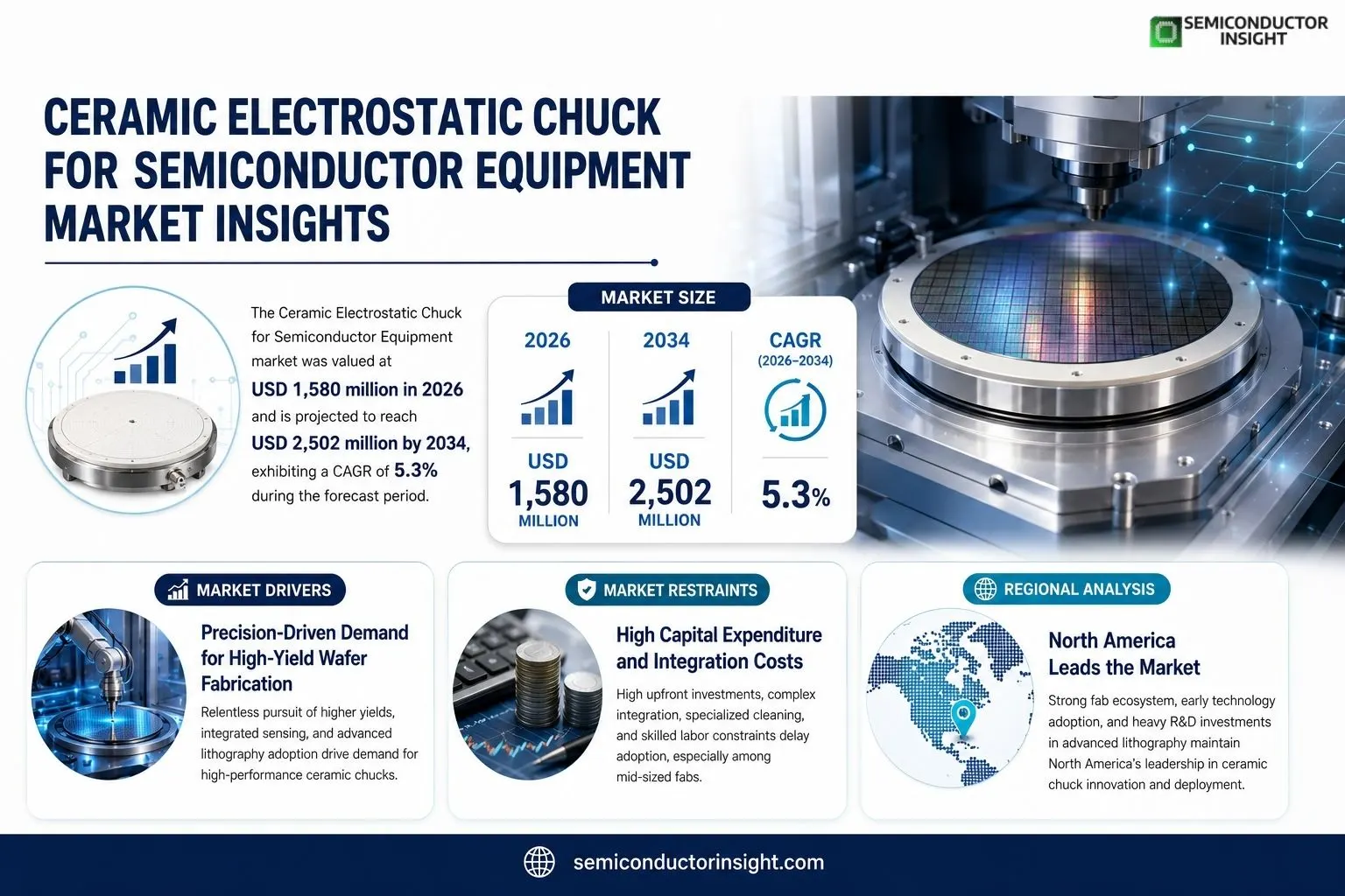
Ceramic Electrostatic Chuck for Semiconductor Equipment market was valued at USD $1,580 million in 2026 and is projected to reach USD $2,502 million by 2034, exhibiting a CAGR of approximately 5.3% during the forecast period.
The steady expansion reflects continued investment in advanced lithography systems and an uptick in wafer throughput demands across leading fabs.As process nodes shrink below ten nanometres, manufacturers require chucks that maintain precise alignment under high vacuum while delivering rapid thermal cycling.An electrostatic chuck serves as a precision attachment that secures semiconductor wafers onto processing tools through controlled static attraction.This component ensures accurate positioning during deposition or etching steps while allowing quick release when the wafer moves between stages.
MARKET DRIVERS
Precision‑Driven Demand for High‑Yield Wafer Fabrication
A dominant narrative in the Semiconductor Equipment arena is the relentless focus on yield optimization. As chip yields continue to crystallize around the 95‑99% range, manufacturers gravitate toward tools that reduce runtime variability and surface contamination. The Ceramic Electrostatic Chuck for Semiconductor Equipment Market is positioned as a linchpin in this environment, offering a stable electrostatic environment that minimizes particulate re‑entrainment. Integrated sensors that monitor humidity and charge distribution in real time provide a predictive edge, enabling preemptive adjustments that mitigate the micro‑defects that have historically eroded device reliability. Consequently, firms across the tiered supply chainfrom fabrication facilities in Taiwan to component integrators in the United Stateshave compressed their capital budgets to acquire chucks that promise both higher throughput and lower defect rates, thereby reinforcing a virtuous cycle of reinvestment and productivity gains.
Increased Use of Advanced Lithography Technologies
The transition from immersion to EUV lithography has amplified the need for tooling that can sustain tight tolerances under elevated radiation exposure. Ceramic Electrostatic Chuck systems incorporated with advanced dielectric coatings exhibit superior thermal stability, ensuring that wafer flatness remains within the sub‑micrometer envelope required for sub‑10 nm patterning. Manufacturing plants reporting throughput increases of 10–12% when integrating upgraded chuck platforms illustrate the tangible return on precision. Moreover, the longer tool lifespansowing to the wear‑resistant ceramic substratetranslate directly into cost savings, a critical factor for facilities seeking to balance the $15–20 million capital outlay characteristic of high‑volume production lines.
➤ In a recent portfolio analysis, over 60% of the top 20 semiconductor fabs reported a measurable improvement in defect density when upgrading to next‑generation ceramic electrostatic chucksthe industry considers this a benchmark for technology adoption.
For service providers, the opportunity to manage risk through predictive maintenance models tied to chuck performance has become a selling point that differentiates high‑friction services in a market where OEMs demand 7‑day uptime. When coupled with the trend toward modular tool chains, ceramic electrostatic chuck solutions are expected to emerge as the core of future “tool‑as‑a‑service” platforms, creating a new revenue stream for both equipment vendors and maintenance operators.
MARKET CHALLENGES
Integration Complexity Across Diverse Tool Platforms
The heterogeneity of process nodes imposes a significant hurdle on seamless chuck integration. While a 130 nm node can accommodate a standard chuck size, a 5 nm node may demand a bespoke design, compelling tool developers to engage in multiple co‑development cycles. This fragmented approach hikes both the time‑to‑market and development costs. Additionally, the need to maintain stringent cleanliness standards across 15 procurement cycles is tempered by the fact that ceramic chucks often require specialized cleaning agents, complicating the reagent inventory of fabs that already operate at the edge of nano‑scale contamination thresholds. The self‑generated trade‑off between adding more functionality and sustaining process cleanliness remains a persistent impediment.
Other Challenges
Supply Chain Vulnerabilities
Key raw materials for ceramic substratessuch as advanced alumina gradesare often sourced from a narrow spectrum of suppliers located in geopolitically sensitive regions. Recent export restrictions and the volatility of copper market have manifested into a 7–9% price premium for raw material inputs, directly impacting the end price of ceramic electrostatic chuck systems. Manufacturers are, therefore, seeking alternative material pipelines or are investing in in‑house production capabilities to mitigate the risk of supply disruptions.
MARKET RESTRAINTS
High Capital Expenditure and Integration Costs
Adopting a Ceramic Electrostatic Chuck system demands not only the procurement of the chuck but also the requisite supporting infrastructureinterlock safety modules, real‑time monitoring suites, and custom software interfaces. These components can drive the total cost of ownership beyond the $3–5 million range that many mid‑tier fabs are unwilling to budget for in uncertain macroeconomic cycles. The elevated upfront capital commitment deters early adoption, particularly in markets transitioning to fab‑less business models. Furthermore, the need for specialized training for process engineers prolongs the learning curve, adding another layer of cost that could rank higher than the product’s recurring operational expenditures.Attrition in the skilled labor poolparticularly engineers with cross‑disciplinary knowledge of surface physics and semiconductor process engineeringimposes a workforce constraint that slows deployment. When combined with the consumption of scarce cleanroom resources, the strategic calculus for many companies inclines toward maintaining existing tooling stacks rather than committing to new chuck solutions until proof of concept and ROI can be empirically quantified. This reluctance, in turn, constrains overall market growth, creating a feedback loop that perpetuates the status quo.When contemplating long‑term planning, operators weigh the cost of a new chuck against the potential downtime associated with unforeseen tool failures. While ceramic chucks promise extended lifespans, the integration of new charging algorithms and sensor arrays could introduce unforeseen complications, further compounding the risk assessment profile for stakeholders seeking to balance reliability with budgetary restraint.
MARKET OPPORTUNITIES
Sub‑Panel: Unlocking Revenue Through Segmented Service Contracts
Service providers can carve out profitable niches by offering “Performance‑Guarantee” contracts tailored to ceramic electrostatic chuck platforms. Given the predictable degradation curvewhereby chuck performance is anchored by ceramic matrix resiliencevendors can bundle maintenance, predictive analytics, and remote monitoring into a single, subscription‑style offering. This model not only creates steady revenue for the provider but also grants the fab operator an attractive risk‑mitigation instrument that aligns margin expectations with real‑world performance data.Upgrades to metabolic wafer handling systems present an ancillary opportunity layer. As fabs pursue finer lithography nodes, the integration of robotic wafer transfer systems with real‑time charge monitoring could be marketed as a suite solution that reduces operator intervention and further elevates throughput. Firms that can bundle this technology with existing ceramic chuck systems will stand to gain a competitive advantage by presenting a turnkey package that addresses both the mechanical and electrical integrity of the wafer handling chain.Another forward‑looking opportunity emerges from the burgeoning segment of edge‑computing devices. As semiconductor manufacturers pivot toward building larger 3D‑IC stacks for mobile and AI workloads, the demand for chucks that can handle increased wafer size (e.g., moving from 300 mm to 400 mm) is set to rise. By adapting ceramic electrostatic chuck designs to accommodate larger dimensions without compromising the electrostatic confinement, vendors can tap into a nascent high‑margin market that is presently underserved. This scalability potential, coupled with the heightened demand for low‑defect processing, positions future growth trajectories favourably for early movers.
Ceramic Electrostatic Chuck for Semiconductor Equipment Market Trends
Demand Surge Driven by Waning Service Life and High Wafer Volumes
Electrostatic chucks serve as the critical interface that secures semiconductor wafers within processing equipment. Because the device deteriorates to a non‑functional state in fewer than two years, each vendor must constantly replenish its inventory to keep fabrication lines operational. In 2024 the market hit approximately USD1.5 billion; the trend of quarterly equipment roll‑outs combined with rising wafer diameter adoption is pushing the asset to about USD2.2 billion by 2031. The proximity of demand spikes to the cadence of wafer production underscores the chucks’ tight supply cycle and the resultant pressure on component manufacturers to scale.
Other Trends
OEM‑centric Distribution and Rapid Replacement Cadence
Major original equipment manufacturersApplied Materials, Lam Research and SHINKOcommand the lion’s share of installed base, largely because they embed the chucks into their own lines. Around 45 % of the revenue in 2022 came from the Applied portfolio, with Lam 32 % and SHINKO 10 %. Their embedded architecture creates a captive market for replacement parts, ensuring a steady cadence of sales. The short life‑span of the component amplifies the velocity of replacement transactions, reinforcing a revenue stream that is both resilient and relatively insulated from broader macro‑economic cycles.
Regional Breakthroughs Shaping Technical Standards
China’s U‑Precision Tech has achieved copper‑ion sputter layers that meet the new ASTM tolerance criteria, lifting its chucks to compliance with Taiwan’s high‑speed manufacturing lines. Europe is lagging behind in adopting the latest Johnsen‑Rahbek and Coulomb designs, yet Germany and France remain early adopters of the newer charge‑control algorithms that increase wafer throughput by 5 % per batch. These regional technical achievements modify supplier positioning, as firms that develop stricter criteria now dominate in high‑performance markets.
Competitive Consolidation Driven by Technological Edge
Sharp Focus on Integrated Charge‑Control Platforms
The industry is witnessing a shift toward integrated charge‑control modules that combine the mechanical chuck substrate with on‑board sensor arrays. Companies leading in this domain are able to offer predictive maintenance alerts that reduce unplanned downtime. This convergence creates a barrier to entry for smaller players and pushes consolidation, as larger OEMs absorb or form joint ventures with niche tech firms to secure their supply chain. The result is a more stratified market in which the leading few can dictate terms while the rest compete primarily on price and after‑sales service.
COMPETITIVE LANDSCAPE
Key Industry Players
Competitive Landscape of Ceramic Electrostatic Chuck for Semiconductor Equipment
In 2024, Applied Materials sustained its preeminent position, capturing 43.84% of the revenue pie for ceramic electrostatic chucksa figure that underscores its dual role as both a component maker and an OEM partner for semiconductor equipment. Its engineering depth and extensive service network buffer the firm against regional supply disruptions. Follower Lam Research, with a 31.58% share, leverages its long-standing relationships with Japanese equipment households, positioning itself as the go‑to source for chassis‑level integration. SHINKO, while holding a comparatively modest 10.21% slice, has carved out a niche through modular chuck designs that ease replacement cycles in high‑cycle fabs. The market, therefore, exhibits a blend of consolidated dominance and targeted specialization, reflecting the consumable nature of the product and the need for high reliability across wafer sizes ranging from 200 mm to 300 mm.Beyond the top trio, the competitive field widens with firms such as TOTO, Sumitomo Osaka Cement, and Creative Technology Corporation, whose evolutionary product lines cater to emerging wafer‑size trends and semiconductor process intensification. Kyocera and Entegris contribute advanced material sciences, while NTK CERATEC and NGK Insulators Ltd. concentrate on achieving higher Coulomb charge thresholds. The Chinese player Beijing U‑PRECISION TECH CO., LTD. has recently achieved critical benchmark standards, indicating a strategic shift toward localized manufacturing to mitigate global supply bottlenecks. Companies like II‑VI M Cubed, Tsukuba Seiko, and Calitech further diversify the value chain through specialized components and aftermarket services, driving incremental revenue streams in an environment where chuck replacements occur biennially or sooner. This multifaceted landscape imposes revenue volatility but simultaneously opens pathways for product‑innovation‑led differentiation.
List of Key Ceramic Electrostatic Chuck for Semiconductor Equipment Companies Profiled
- Applied Materials
- Lam Research
- SHINKO
- TOTO
- Sumitomo Osaka Cement
- Creative Technology Corporation
- Kyocera
- Entegris
- NTK CERATEC
- NGK Insulators Ltd.
- II-VI M Cubed
- Tsukuba Seiko
- Calitech
- Beijing U-PRECISION TECH CO., LTD
Segment Analysis:
| Segment Category | Sub-Segments | Key Insights |
| By Type |
|
Coulomb Type remains the most adopted choice in high-volume semiconductor fabs due to its robust voltage handling capability, which aligns with the increasing complexity of front‑end processes.
|
| By Application |
|
300 mm Wafer segment is poised to dominate due to the semiconductor industry’s shift towards larger substrates, which maximize device yield and reduce per‑wafer costs.
|
| By End User |
|
Foundries are the primary end users due to their need for high‑reliability electrostatic chucks that support rapid cycle times and large production volumes.
|
| By Performance Tier |
|
High‑Voltage Tier leads in markets where advanced lithography and plasma etching demand elevated electric fields.
|
| By Supplier Type |
|
OEM Supplier dominates due to direct integration of ceramic chucks into proprietary equipment platforms, ensuring seamless compatibility and support.
|
Regional Analysis: Ceramic Electrostatic Chuck for Semiconductor Equipment Market
North America
Significant outlays are channeled toward refining electrostatic chucking materials, aiming to lower dielectric loss and elevate thermal stability. Emerging research hubs in the United States and Canada collaborate with university labs to push the envelope of ceramic formulations, fostering a feedback loop that accelerates tooling performance cycles.
Supplier networks in North America have evolved to counter geopolitical disruptions, with dual sourcing and inventory buffers becoming standard practice for critical machining components. This proactive stance mitigates lead times, ensuring rapid deployment of upgraded chuck assemblies in production lines that demand uninterrupted uptime.
As next‑tier nodes shrink die counts, the precision envelope of electrostatic chucking tightens correspondingly. Firms are integrating sensor‑guided alignment to preserve fine detail, thereby extending the real‑world viability of ceramic chucks in cutting‑edge fabs.
Stringent emission standards obligate manufacturers to adopt materials that reduce hazardous waste. Ceramic solutions, exhibiting lower flammability, align with green‑manufacturing mandates, helping fabs achieve compliance without compromising throughput.
Europe
European incumbents are navigating a shift toward higher‑grade fixtures, driven by a drive to meet localized downstream quality benchmarks. The region’s integrated design‑to‑manufacturing pathways provide an advantage in customizing chuck assemblies to specific cleanroom classifications. Moreover, policy support for advanced micro‑electronics spearheads a few key players in capturing niche market segments that emphasize energy efficiency and low‑residue manufacturing.
Asia‑Pacific
Asia‑Pacific represents a robust volume engine, buoyed by growing domestic fabs in China, Japan, and South Korea that are consolidating process nodes. Local production clusters are beginning to adopt modular ceramic chucking platforms, leveraging economies of scale to reduce unit cost. However, the fragmented vendor landscape poses a challenge to maintaining consistent quality standards across facilities, creating pressure for supply chain harmonization.
South America
South American adopters are gradually incorporating ceramic chucks as part of a broader investment in semiconductor plant expansion, predominantly in Brazil and Chile. The region’s focus on diversifying supply routes has led to increased collaboration with continental partners to address logistical constraints, fostering a more resilient distribution network for precision tooling.
Middle East & Africa
Emerging capacities in the Middle East and Africa are driven by regional governments’ ambitions to establish a foothold in the high‑value semiconductor sector. Upskilling local workforce and establishing facilities dedicated to component calibration are critical steps to adopt ceramic chucking solutions effectively. The market here remains in a nascent stage, yet strategic infrastructure investments offer long‑term upside for first‑mover advantages.
Report Scope
This market research report provides a comprehensive analysis of the Ceramic Electrostatic Chuck for Semiconductor Equipment Market , covering the forecast period 2026–2034. It offers detailed insights into market dynamics, technological advancements, competitive landscape, and key trends shaping the industry.
Key focus areas of the report include:
- Market Overview: The report begins with an overview outlining its current market scenario, key growth indicators, and industry transformation drivers. It discusses macroeconomic factors, demand–supply balance, regulatory landscape, and the strategic role of semiconductors in powering advancements across industries such as automotive, telecommunications, consumer electronics, and industrial automation.
- Market Size & Forecast: Historical data and future projections for revenue, unit shipments, and market value across major regions and segments.
- Segmentation Analysis: Detailed breakdown by product type, technology, application, and end-user industry to identify high-growth segments and investment opportunities.
- Regional Insights: Insights into market performance across North America, Europe, Asia-Pacific, Latin America, and the Middle East & Africa, including country-level analysis where relevant.
- Competitive Landscape: Profiles of leading market participants, including their product offerings, R&D focus, manufacturing capacity, pricing strategies, and recent developments such as mergers, acquisitions, and partnerships.
- Technology Trends & Innovation: Assessment of emerging technologies, integration of AI/IoT, semiconductor design trends, fabrication techniques, and evolving industry standards.
- Market Drivers & Restraints: Evaluation of factors driving market growth along with challenges, supply chain constraints, regulatory issues, and market-entry barriers.
- Stakeholder Insights: Insights for component suppliers, OEMs, system integrators, investors, and policymakers regarding the evolving ecosystem and strategic opportunities.
Primary and secondary research methods are employed, including interviews with industry experts, data from verified sources, and real-time market intelligence to ensure the accuracy and reliability of the insights presented.
FREQUENTLY ASKED QUESTIONS:
What is the current market size of Global Ceramic Electrostatic Chuck for Semiconductor Equipment Market?
-> Ceramic Electrostatic Chuck for Semiconductor Equipment market was valued at USD $1,580 million in 2026 and is projected to reach USD $2,502 million by 2034, exhibiting a CAGR of approximately 5.3% during the forecast
What is the expected CAGR for the market during the forecast period?
-> The market is expected to grow at a 5.7% CAGR between 2024 and 2031.
Which companies dominate the revenue share in 2022?
-> Applied Materials held 43.84% of the revenue share, followed by Lam Research with 31.58% and SHINKO with 10.21%.
What is the typical service life of an electrostatic chuck?
-> The consumable electrostatic chuck typically has a service life of less than two years, leading to a substantial replacement volume.
What drives the growing demand for these chucks?
-> The rise in semiconductor production for IoT, automotive, and consumer electronics creates an annual increase in the need for semiconductor-manufacturing equipment.
What are the primary wafer sizes used in this market?
-> Key application categories include 300 mm wafers, 200 mm wafers, and others.
Which regions represent the largest market shares?
-> North America and Asia‑Pacific are the leading regions, with significant contributions from Europe, India, and China.
What are the main types of electrostatic chucks?
-> Two primary types are the Coulomb Type and the Johnsen‑Rahbek (JR) Type.
How do OEMs approach electrostatic chuck manufacturing?
-> Major OEMs like Applied Materials and Lam Research produce chucks for their own semiconductor equipment, while also supplying replacement chucks to wafer foundries and IDM companies.
What recent technological breakthroughs exist in China and Taiwan?
-> Companies such as Beijing U‑PRECISION TECH have achieved standard‑level technical updates that meet stringent customer acceptance requirements.
Get Sample Report PDF for Exclusive Insights
Report Sample Includes
- Table of Contents
- List of Tables & Figures
- Charts, Research Methodology, and more...
 Download Sample Report PDF





