
Wafer Handling Equipment Market Insights
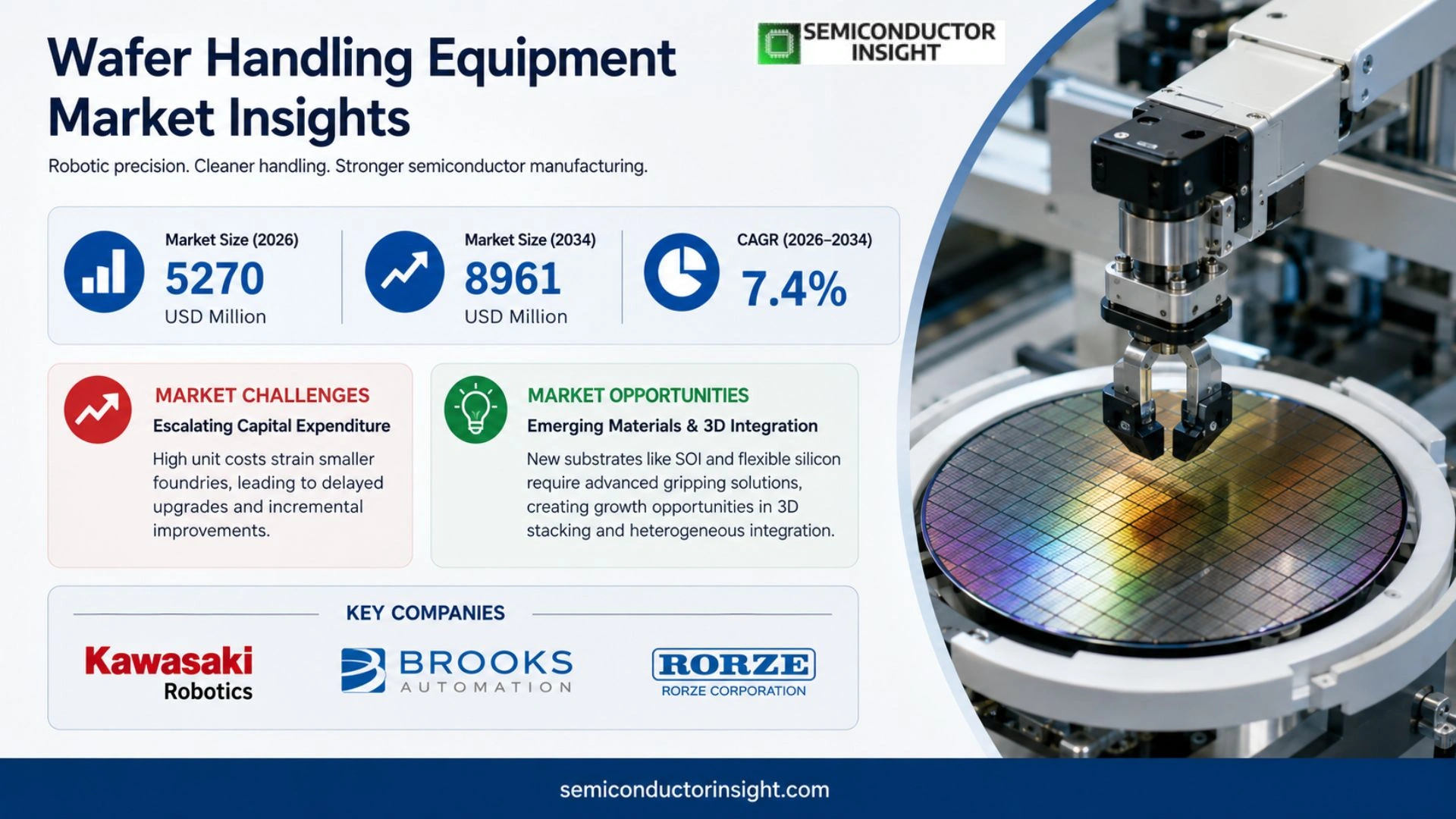
Wafer Handling Equipment market is expected to rise from USD 5270 million in 2026 to USD 8961 million by 2034, showing a CAGR of 7.4 % over the forecast horizon.
Wafer Handling Equipment comprises the automation hardware stack that enables carrier (FOUP/FOSB/cassette) and wafer transfer, positioning, buffering, and exchange between factory logistics and process tools, as well as within multi‑module tools. It is commonly described across three layers: (1) factory‑level AMHS for in‑fab storage and transport; (2) tool front‑end modules (EFEM) that link carrier transport with process tools; and (3) in‑tool transfer robots that move wafers among load locks, chambers, and internal buffers.
The sector’s expansion stems from rising fab automation density, tighter contamination controls required for sub‑10 nm nodes, and increasing standardisation of load‑port interfaces such as SEMI E15 and E87. Moreover, manufacturers are investing heavily in mini‑environment integration and edge‑grip handling solutions to protect wafer backside cleanliness. Recent announcements include new OHT platforms from leading OEMs announced in Q2 2024 aimed at supporting high‑throughput 300 mm fabs.
MARKET DRIVERS
Rising Demand for High‑Yield Semiconductor Production
Manufacturers are tightening yield tolerances as device architectures shrink below 10 nm. Wafer Handling Equipment market benefits because fabs must replace legacy handlers with systems that guarantee sub‑micron positional accuracy and reduced particle generation. Operators are willing to invest in equipment that demonstrably trims defect density, because each percentage point gain in yield translates directly into revenue uplift.
Automation and Industry 4.0 Integration
Smart sensors, real‑time data analytics, and closed‑loop robotic control are moving from pilot projects to production lines. Companies that embed predictive maintenance within wafer handlers can pre‑empt downtime, a factor that directly improves fab utilization. The shift toward fully automated wafer flow creates a clear preference for equipment that can communicate seamlessly with Manufacturing Execution Systems.
➤ Operators report a 12 % reduction in cycle time after retrofitting existing handlers with AI‑driven alignment modules.
These dynamics compel equipment suppliers to accelerate R&D pipelines, while also expanding service networks that can quickly certify new automation modules. The net effect is a steady uplift in capital orders across both mature and emerging fab locations.
MARKET CHALLENGES
Escalating Capital Expenditure
Advanced wafer handling platforms often exceed $2 million per unit, a price point that strains the budgets of smaller foundries. When investment decisions are weighed against tight operating margins, firms may postpone upgrades, favoring incremental improvements over wholesale replacement.
Other Challenges
Supply Chain Volatility
Component shortages for high‑precision linear motors and vacuum subsystems have introduced lead‑time extensions of up to six months. The ripple effect forces purchasers to lock in prices early, limiting flexibility in responding to technology shifts.
MARKET RESTRAINTS
Stringent Cleanroom Compliance
Compliance with Class 1 or better cleanroom standards mandates rigorous material selection and outgassing controls for every component of a wafer handler. Vendors must undergo extensive qualification, a process that adds both time and cost to product roll‑out, tempering market velocity.
Limited Standardization Across Facilities
Different fab operators adopt a variety of carrier and chuck formats, hindering the development of truly universal handling solutions. This fragmentation forces equipment makers to maintain multiple product variants, diluting economies of scale and increasing inventory complexity.
MARKET OPPORTUNITIES
Emerging Materials and 3D Integration
New substrate materials such as silicon‑on‑insulator (SOI) and flexible silicon demand customized gripping mechanisms to avoid micro‑cracking. Suppliers that engineer adaptive clamping systems stand to capture early‑stage contracts from companies pioneering 3D stacking and heterogeneous integration.
Aftermarket Services and Retrofit Solutions
Many fabs operate legacy handlers that lack modern sensor suites. Offering retrofit kits that embed vision‑based alignment and remote diagnostic capabilities creates a recurring revenue stream and extends equipment lifespan, a proposition that resonates with cost‑conscious operators.
Geographic Expansion in Emerging Semiconductor Hubs
Regions such as Southeast Asia and Eastern Europe are attracting new fabs due to favorable policy incentives. Establishing local engineering and support centers in these zones can reduce service response times, making suppliers more attractive to emerging players.
Wafer Handling Equipment Market Trends
Automation Density and Mini‑Environment Penetration
Wafer Handling Equipment market is seeing a pronounced shift toward higher automation density within 300 mm fabs. As fabs expand their footprint and introduce more process modules, the need for continuous wafer transport across longer interbay tracks becomes critical. Vendors are embedding larger fleets of overhead transport vehicles and integrating buffer stations that operate round‑the‑clock, reducing idle time between deposition, etch, and inspection steps. Simultaneously, mini‑environment enclosures are moving from optional add‑ons to standard components of EFEMs and sorters. By tightly controlling temperature, particle count, and humidity around the wafer carrier, these enclosures directly address the tighter contamination budgets demanded by sub‑10 nm node devices. The combined effect is a measurable lift in tool throughput and a reduction in wafer‑loss incidents, reshaping capacity planning for fab managers.
Other Trends
Standardized Load‑Port and Carrier Interfaces
Standardization, codified in SEMI E15 and E87, now underpins most equipment procurement decisions. Uniform load‑port dimensions and docking mechanisms enable seamless hand‑off between AMHS, EFEMs, and cluster‑tool robots. This interoperability lowers integration costs and accelerates line‑upgrade cycles, because a single carrier type can travel the entire fab without custom adapters. For suppliers, the push toward modularity translates into product portfolios that emphasize interchangeable front‑end modules, offering customers the flexibility to retrofit existing lines while preserving compliance with evolving clean‑room standards.
Lights‑Out Fab Objectives Driving Predictive Maintenance
Operators are targeting “lights‑out” production where human intervention is limited to exception handling. To realize this, Wafer Handling Equipment market is embedding advanced diagnostics into motion controllers, encoders, and vacuum robots. Real‑time vibration analysis and sensor‑fusion algorithms feed predictive‑maintenance platforms that schedule component replacements before failure, thereby shrinking mean‑time‑to‑repair (MTTR). The ripple effect is twofold: first, it safeguards the high‑value wafer stream from unexpected pauses; second, it creates a data‑rich environment where AI‑driven scheduling can dynamically re‑route wafers, optimizing line balance across multiple tool families.
COMPETITIVE LANDSCAPE
Key Industry Players
Wafer Handling Equipment Market – Competitive Overview
The wafer handling segment is dominated by a handful of multinational firms that couple deep semiconductor expertise with advanced robotics. Brooks Automation, for instance, leverages its legacy in vacuum robotics to supply integrated EFEM and intra‑tool transfer solutions across the 300 mm ecosystem, allowing fabs to compress cycle times while preserving yield. Kawasaki Robotics complements this position with high‑speed overhead transport (OHT) platforms and modular load‑port architectures that are widely adopted in Tier‑1 foundries. Both companies have pursued strategic acquisitions,Brooks’ purchase of Genmark Automation and Kawasaki’s joint venture with a leading wafer‑sorter provider,to broaden their product portfolios and lock in long‑term service contracts. Their global footprint, backed by extensive aftermarket networks, translates into a market share that eclipses smaller suppliers, making them the primary reference points for fab planners seeking end‑to‑end automation.
Beyond the top tier, a diverse set of niche specialists fuels innovation in discrete sub‑segments. Companies such as RORZE Corporation and DAIHEN Corporation concentrate on precision motion control and mini‑environment modules, attributes that are increasingly valued as wafer geometries shrink and contamination tolerances tighten. Regional players like Shanghai Guona Semiconductor and Mirle Automation have capitalized on the rapid fab expansions in China and Southeast Asia, offering cost‑effective OHT solutions that integrate seamlessly with locally dominant AMHS software stacks. Meanwhile, firms such as Stäubli and EPSON Robots provide high‑precision wafer‑transfer robots that cater to advanced packaging and heterogenous integration lines. These smaller outfits often differentiate themselves through bespoke engineering services, rapid prototyping cycles, and close collaborations with equipment OEMs, creating a competitive pressure that pushes incumbents toward continuous product refinement.
List of Key Wafer Handling Equipment Companies Profiled
- Kawasaki Robotics
- Brooks Automation
- RORZE Corporation
- DAIHEN Corporation
- Yaskawa
- Sumitomo Heavy Industries (SHI)
- Robostar
- Mirle Automation
- Stäubli
- EPSON Robots
- Daifuku
- ULVAC
- Sinfonia Technology
- SMCore
- Shanghai Guona Semiconductor
Segment Analysis:
| Segment Category | Sub-Segments | Key Insights |
| By Type |
|
EFEM & Sorter serves as the central hub linking carrier transport to process tools, enabling precise wafer positioning and contamination control. – Enhances yield by minimizing manual handling errors. – Integrates mini‑environment modules that protect wafer surfaces during transfer. – Provides modular interfaces that support rapid tool upgrades and flexible fab layouts. – Aligns with industry standards (SEMI E87/E90) fostering interoperability across equipment suppliers. |
| By Application |
|
Etching Equipment relies heavily on precise wafer handling to sustain high‑volume throughput while preserving pattern fidelity. – Vacuum‑based robots provide rapid, repeatable wafer exchange within cluster tools. – Tight integration with load‑port standards reduces cycle time and contamination risk. – Supports “lights‑out” fab concepts by enabling autonomous, unattended wafer movement. – Facilitates advanced process control through real‑time telemetry linking handling modules to fab MES systems. |
| By End User |
|
Fab Operators drive the adoption of advanced handling solutions to meet escalating yield and throughput expectations. – Prioritize equipment that offers seamless integration with existing AMHS infrastructure. – Demand robust safety interlocks and predictive maintenance analytics to reduce downtime. – Emphasize clean‑room compatibility, especially edge‑grip handling for backside contamination control. – Seek modular systems that can evolve with fab expansion plans without extensive re‑engineering. |
| By Technology |
|
Vacuum Robots dominate in‑tool transfer environments where high‑precision, contamination‑free movement is critical. – Provide rapid wafer exchange between load‑locks and process chambers, supporting complex multi‑step recipes. – Integrated sensor suites enable real‑time alignment and slot‑mapping, improving throughput consistency. – Compatibility with standard SECS/GEM communication simplifies integration across tool families. – Their proven reliability makes them a preferred choice for high‑value processes such as etch and deposition. |
| By Process Stage |
|
In‑Tool Transfer is pivotal for maintaining process continuity and minimizing wafer exposure to contaminants. – Enables seamless handoff between load‑ports, buffer stations, and processing modules. – Drives higher equipment utilization by reducing idle time between steps. – Incorporates advanced alignment and vision systems that guarantee positional accuracy for sub‑micron features. – Supports the shift toward fully automated, “lights‑out” fabs where human interaction is minimized. |
Regional Analysis: Wafer Handling Equipment Market
Asia‑Pacific
Leading wafer fabs are scaling capacity to meet demand for high‑density chips, prompting equipment vendors to accelerate production schedules. The emphasis on modular designs enables swift line upgrades, allowing operators to insert new handling stations without extensive plant downtime. This approach aligns with the region’s aggressive roadmap for advanced logic and memory devices.
Automation, robotics, and AI‑driven inspection are becoming integral to wafer handling workflows. Suppliers that embed predictive maintenance algorithms gain a competitive edge, as they can promise higher throughput and lower defect rates – critical metrics for fabs targeting sub‑5nm processes.
Recent disruptions have led manufacturers to diversify component sources and increase on‑site inventories of critical handling modules. This shift reduces reliance on single‑supplier pipelines and shortens lead times for critical upgrades, reinforcing operational stability across the region.
Environmental compliance frameworks are tightening, with emphasis on reducing chemical usage in wafer transfer processes. Companies that can demonstrate lower ecological footprints while maintaining precision are better positioned to secure long‑term contracts with environmentally conscious fab operators.
North America
North America remains a strong secondary market for Wafer Handling Equipment, driven largely by the United States’ mature fabs and a growing ecosystem of research facilities. The region benefits from deep pockets of venture capital that fund niche equipment startups focused on niche processes such as quantum and photonic chips. However, the market’s tempo is moderated by longer equipment replacement cycles and a more cautious capital‑allocation mindset compared with Asia‑Pacific. Strategic partnerships between equipment manufacturers and domestic semiconductor consortia help mitigate these constraints, offering avenues for co‑development that align technology roadmaps with regional demand patterns.
Europe
European wafer handling vendors face a landscape shaped by stringent environmental standards and a fragmented customer base across several mature economies. The region’s emphasis on sustainability drives innovation in low‑emission handling tools and closed‑loop coolant systems. While overall demand is steadier than in the Asia‑Pacific, the presence of high‑value specialty fabs,particularly in Germany and the Netherlands,creates pockets of premium‑price opportunities for equipment capable of supporting heterogeneous integration and advanced packaging techniques.
South America
South America’s contribution to Wafer Handling Equipment market is modest but evolving, as several nations launch initiatives to attract semiconductor investment. Government incentives aimed at building pilot fabs have sparked preliminary interest from equipment providers willing to offer customized solutions that accommodate lower production volumes. The principal challenge remains the development of a skilled workforce capable of operating sophisticated handling systems, prompting firms to bundle training programs with equipment sales to accelerate market uptake.
Middle East & Africa
The Middle East & Africa region is at an early stage of participation in Wafer Handling Equipment market. Investment in semiconductor manufacturing is nascent, yet strategic vision documents from several Gulf states outline ambitions to establish downstream processing capabilities. Equipment manufacturers are positioning themselves as partners in these long‑term plans by offering scalable handling platforms that can be expanded as local fabs mature. Collaborative ventures with regional universities aim to cultivate the technical expertise required to sustain future equipment deployment.
Report Scope
This market research report provides a comprehensive analysis of the Wafer Handling Equipment Market , covering the forecast period 2026–2034. It offers detailed insights into market dynamics, technological advancements, competitive landscape, and key trends shaping the industry.
Key focus areas of the report include:
- Market Overview: The report begins with an overview outlining its current market scenario, key growth indicators, and industry transformation drivers. It discusses macroeconomic factors, demand–supply balance, regulatory landscape, and the strategic role of semiconductors in powering advancements across industries such as automotive, telecommunications, consumer electronics, and industrial automation.
- Market Size & Forecast: Historical data and future projections for revenue, unit shipments, and market value across major regions and segments.
- Segmentation Analysis: Detailed breakdown by product type, technology, application, and end-user industry to identify high-growth segments and investment opportunities.
- Regional Insights: Insights into market performance across North America, Europe, Asia-Pacific, Latin America, and the Middle East & Africa, including country-level analysis where relevant.
- Competitive Landscape: Profiles of leading market participants, including their product offerings, R&D focus, manufacturing capacity, pricing strategies, and recent developments such as mergers, acquisitions, and partnerships.
- Technology Trends & Innovation: Assessment of emerging technologies, integration of AI/IoT, semiconductor design trends, fabrication techniques, and evolving industry standards.
- Market Drivers & Restraints: Evaluation of factors driving market growth along with challenges, supply chain constraints, regulatory issues, and market-entry barriers.
- Stakeholder Insights: Insights for component suppliers, OEMs, system integrators, investors, and policymakers regarding the evolving ecosystem and strategic opportunities.
Primary and secondary research methods are employed, including interviews with industry experts, data from verified sources, and real-time market intelligence to ensure the accuracy and reliability of the insights presented.
FREQUENTLY ASKED QUESTIONS:
What is the current market size of Wafer Handling Equipment Market?
-> Wafer Handling Equipment market is expected to rise from USD 5270 million in 2026 to USD 8961 million by 2034, showing a CAGR of 7.4 %
Which key companies operate in Wafer Handling Equipment Market?
-> Key players include Kawasaki Robotics, RORZE Corporation, Brooks Automation, DAIHEN Corporation, Hirata Corporation, Yaskawa, Nidec (Genmark Automation), JEL Corporation, Robostar, Robots and Design (RND), among others.
What are the key growth drivers?
-> Key growth drivers include higher automation density driven by fab expansions, tighter contamination and yield requirements, stronger standardization and interoperability demands, and “lights‑out” productivity goals for higher throughput and predictive maintenance.
Which region dominates the market?
-> Asia dominates Wafer Handling Equipment market, with China, Japan and South Korea leading in adoption and installed capacity.
What are the emerging trends?
-> Emerging trends include increased mini‑environment penetration, edge‑grip handling for backside cleanliness, AI‑enabled wafer transfer robots, and integration of predictive maintenance diagnostics.

Get Sample Report PDF for Exclusive Insights
Report Sample Includes
- Table of Contents
- List of Tables & Figures
- Charts, Research Methodology, and more...
 Download Sample Report PDF




