Key Statistics
Key Takeaways
- USD 19,970 million in 2025 establishes a large wafer-fabrication equipment market whose demand is tied directly to the number of 200mm and 300mm fabs, process steps per wafer and the complexity of pattern transfer. The equipment category includes dry and wet etch systems, with dry plasma-based technology providing the core platform for advanced logic, memory and high-aspect-ratio structures.
- Dry etch is the dominant technology family for advanced semiconductor manufacturing as plasma systems can deliver anisotropic removal and tighter profile control than conventional wet processes. Lam Research’s portfolio spans conductor etch, atomic-layer etch, cryogenic processes, deep reactive ion etch and selective etch, illustrating how process-specific tool architectures are expanding as structures become taller, narrower and more material-diverse.
- Logic and memory are the principal application engines, supported by continued AI-server, advanced-node, HBM and 3D-memory investment. SEMI projects global 300mm fab-equipment spending at USD 133 billion in 2026 and USD 151 billion in 2027. That equipment environment creates a direct pipeline for etch chambers, process modules, service contracts and upgraded platforms designed around critical-dimension control.
- Five-nanometre-and-below process development carries the strongest technology intensity, even though mature nodes and power devices remain meaningful demand pools. Tokyo Electron’s 2026 etch technology guide shows how new process approaches can materially change silicon and silicon-oxide etch outcomes in logic and DRAM structures. Suppliers therefore compete on plasma physics, endpoint control, chamber condition and selective removal rather than only on throughput.
- Asia Pacific remains the largest market, while North America has the strongest near-term expansion pipeline. Lam Research’s June 2026 revenue geography included 27% Taiwan, 26% China and 20% Korea, demonstrating the concentration of manufacturing activity. At the same time, TSMC, Intel and Micron are expanding U.S. capacity, creating new qualification and installation opportunities for etch equipment suppliers.
Semiconductor Etch Equipment Market Overview
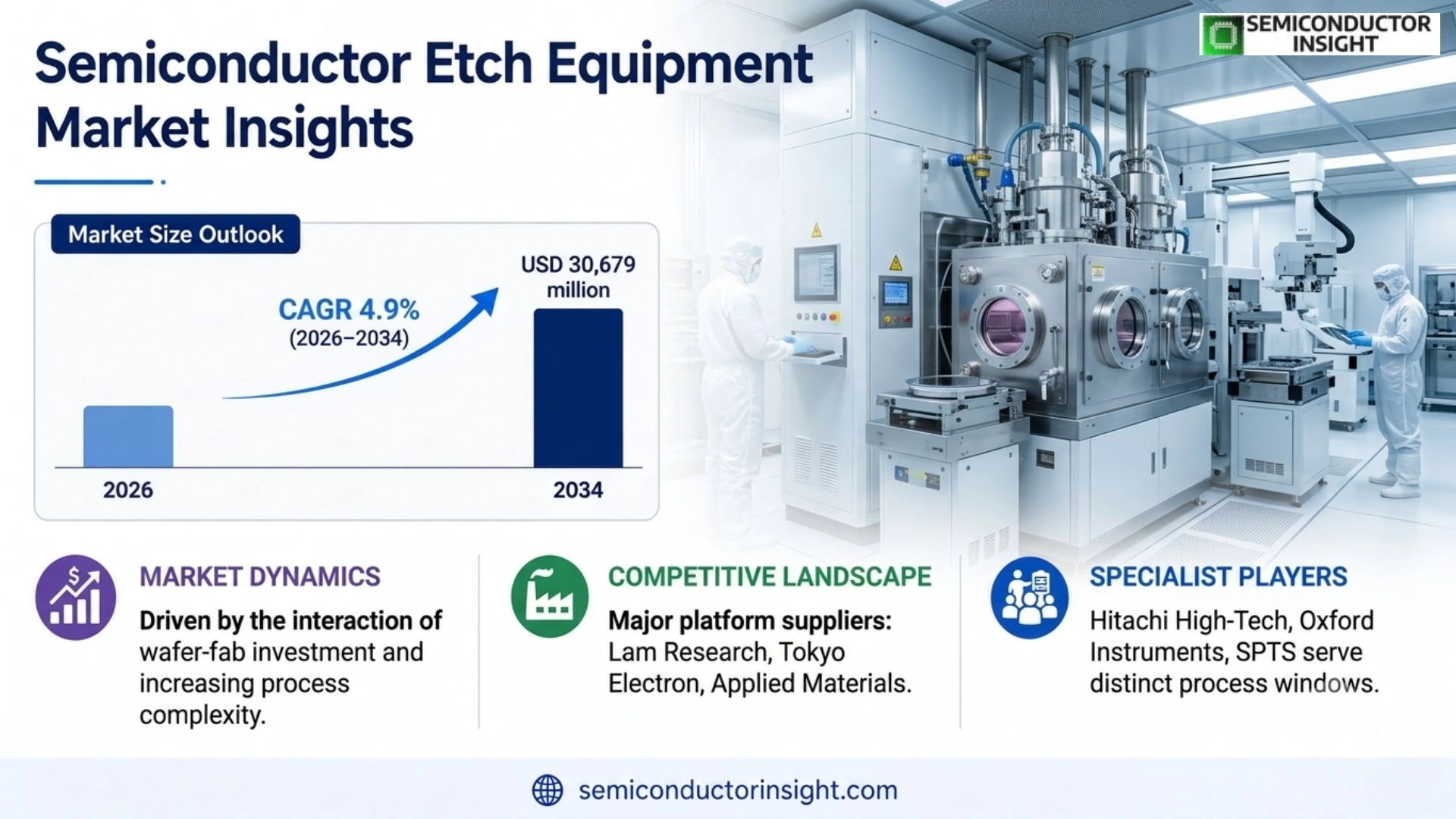
semiconductor etch equipment market was valued at USD 19,970 million in 2025. Using the published 2025 and 2033 anchors and extending the same implied growth factor to 2034, the market reaches approximately USD 30,679 million in 2034, equivalent to a 4.9% CAGR for 2026–2034. The market covers dry and wet etch equipment used by foundries, IDMs and OSAT providers across logic and memory, power devices, MEMS and other specialty process flows.
Etch equipment removes selected portions of semiconductor films to transfer lithographic patterns into underlying layers. In advanced manufacturing, etch is not one operation but a family of controlled processes differentiated by material, feature geometry, aspect ratio, selectivity, profile and endpoint. Dry plasma systems dominate the most demanding pattern-transfer tasks, while wet etch remains important where liquid chemistry provides useful selectivity, throughput or surface-treatment economics. The equipment therefore combines chamber hardware, gas delivery, RF power, temperature management, vacuum, endpoint sensing and process software.
The shift toward gate-all-around logic, multilayer memory, HBM, advanced packaging and three-dimensional device structures is increasing the number of places where etch performance can determine yield. A taller structure can require repeated etch and passivation cycles, tighter sidewall control and more selective removal between adjacent materials. Lam Research’s process portfolio includes atomic-layer etch, cryogenic etch, conductor etch and deep reactive ion etch, reflecting a move toward highly specialized process modules rather than one universal chamber architecture.
Capital spending provides the main demand signal. SEMI projected worldwide 300mm fab-equipment spending of USD 133 billion in 2026, USD 151 billion in 2027, USD 155 billion in 2028 and USD 172 billion in 2029. Earlier SEMI work put 2025 spending at USD 107 billion and 2026 at USD 116 billion across a different forecast vintage. These figures describe the wider equipment environment rather than etch alone, but they matter directly as etch is one of the recurring tool categories purchased whenever new wafer-fab capacity and advanced-node conversions are installed.
The commercial model also includes substantial recurring value after the initial system sale. Etch chambers accumulate deposits, consumable liners and process drift, creating demand for chamber parts, refurbishment, service, process upgrades and software. Lam Research’s June 2026 quarter illustrates the scale of this installed-base model: systems revenue was about USD 4.25 billion while customer-support revenue was about USD 2.47 billion. The exact mix includes several wafer-fabrication equipment categories, yet it demonstrates how a large installed base can support service revenue alongside new tool shipments.
Segment Analysis: By Type
The report’s type segmentation contains two categories: Dry Etch Equipment and Wet Etch Equipment. Dry etch is the leading technology family for advanced pattern transfer, especially in logic and memory, while wet etch remains indispensable for high-selectivity removal and specialty processes. The purchasing trigger is process geometry. As critical dimensions shrink or aspect ratios rise, buyers increasingly value anisotropy, selectivity and repeatability, which pushes investment toward more sophisticated plasma chambers, gas systems, endpoint control and chamber-condition management.
| Type | Technical and purchasing logic | Commercial position |
|---|---|---|
| Dry Etch Equipment | Dry etch uses plasma or reactive species to remove selected materials with high anisotropy and control of critical dimensions. Lam Research lists conductor etch, atomic-layer etch, cryogenic and deep reactive ion etch families, while Applied Materials continues to develop selective etch for high-aspect-ratio structures. Advanced logic, DRAM and 3D NAND increasingly require process windows that make chamber chemistry, plasma control and endpoint precision strategic. | Dominant technology family for advanced-node and 3D pattern transfer; highest technology intensity. |
| Wet Etch Equipment | Wet etch uses liquid chemistries to selectively remove films and process residues, often where isotropic removal or high throughput provides an economic advantage. It remains relevant across cleaning, surface preparation, bulk material removal and specialty process steps. Equipment suppliers compete on chemical delivery, temperature control, particle management, automation and compatibility with increasingly sensitive materials, while fabs weigh throughput against selectivity and contamination control. | Important complementary technology where chemical selectivity, throughput and surface preparation are advantageous. |
Which technical axis creates the greatest equipment differentiation?
Aspect-ratio control and selective removal increasingly determine etch differentiation. TEL’s May 2026 technology guide compares conventional and new process approaches for DRAM capacitor SiO2 etch and logic gate silicon etch, illustrating how a change in process chemistry or plasma condition can materially alter bottom critical dimension and residual silicon. The purchasing decision is therefore increasingly tied to process capability at the customer’s target node, not simply chamber throughput or installed system count.
Segment Analysis: By Application
The application axis includes Logic and Memory, Power Device, MEMS and Others. Logic and memory form the principal demand pool as leading-edge architectures require multiple pattern-transfer stages and increasingly selective etch. Power devices and MEMS create a different kind of value, with deeper structures, difficult materials and specialized profile requirements. The application purchasing trigger is therefore not just wafer volume: it is the complexity of the feature geometry and the cost of a profile excursion in a particular device family.
| Application | Demand characteristics and purchasing trigger |
|---|---|
| Logic and Memory | Logic and memory form the largest application pool as advanced processors, HBM-connected systems and high-density memory arrays require repeated pattern transfer and increasingly selective etch steps. SEMI expects global 300mm fab equipment spending to reach USD 133 billion in 2026 and USD 151 billion in 2027, providing the capital backdrop for continued etch equipment demand. Suppliers therefore optimize products around critical-dimension control, high aspect ratios and stable multi-step process sequences. |
| Power Device | Power semiconductors use etch across silicon carbide, silicon and other device structures where deep features, hard materials and high-voltage architectures can create unusually demanding process windows. Suppliers must balance etch rate with sidewall integrity and defect control. The market opportunity is driven by electrification and power conversion rather than only by advanced-node scaling, so equipment platforms need process flexibility across multiple wafer materials and device geometries. |
| MEMS | MEMS fabrication uses etch to create cavities, trenches, membranes and other three-dimensional structures, often combining anisotropic plasma processes with silicon deep reactive ion etching. Lam’s DRIE and RIE portfolio illustrates the equipment breadth required. Purchasing decisions emphasize feature depth, sidewall quality, wafer bow tolerance and recipe flexibility, while device makers frequently value application engineering that can adapt a platform to distinct sensor architectures. |
| Others | The Others category includes specialty semiconductors and process flows that do not fit the main logic, memory, power or MEMS groups. It can include compound-semiconductor, photonics and heterogeneous-integration processes where material stacks differ from mainstream CMOS. Suppliers gain by offering modular chambers and recipes that can be qualified across lower-volume applications, allowing customers to use established platforms without accepting the cost of a fully bespoke etch architecture. |
How does the application mix change the tool specification?
Logic and memory buyers often prioritize nanometre-scale critical-dimension control, selective material removal, chamber matching and defect performance across many wafers. Power-device fabs may place greater emphasis on deep etch capability, hard-material processing and robustness across larger feature sizes. MEMS manufacturers can prioritize silicon DRIE, sidewall profile and wafer bow tolerance. These differences favor modular platforms whose chambers, gas systems and recipes can be optimized for several device families without forcing the customer into completely separate equipment infrastructures.
Regional Analysis
Asia Pacific is the largest regional etch equipment market through the concentration of logic, memory and foundry manufacturing across Taiwan, Korea, China and Japan. North America is the fastest-developing expansion region as the United States adds leading-edge logic and memory capacity. Europe is project-led through Chips Act-supported manufacturing, while South America and the Middle East & Africa remain smaller markets tied to specialty production, research and emerging industrial clusters.
Where is etch equipment demand strongest, and where is capacity localization accelerating fastest?
| Region | Current position | Growth mechanism | Supplier ecosystem | Commercial implication |
|---|---|---|---|---|
| Asia Pacific | Asia Pacific is the largest demand center as it hosts the highest concentration of semiconductor wafer-fabrication capacity and the broadest installed base of advanced process equipment. Taiwan, Korea, China and Japan combine major fabs with equipment, materials and service ecosystems. Lam Research’s June 2026 revenue geography included 27% Taiwan, 26% China and 20% Korea, showing the weight of these manufacturing locations in a leading equipment supplier’s business. | Advanced logic, memory and 3D-device investment adds chambers, process modules and service needs. Mature-node expansion preserves demand for established platforms, while advanced-node conversion increases the value of selective and high-aspect-ratio etch. | Local equipment service, process engineering and component support have become critical as fabs run complex multi-chamber production lines. New tool installations are typically paired with long-duration support and upgrade requirements. | Suppliers should maintain regional field engineering, spare-parts inventory and application labs close to the major clusters. Qualification strength and installed-base service are major barriers to substitution. |
| North America | North America has the strongest near-term expansion pipeline as leading-edge logic and memory manufacturing is being localized in the United States. TSMC Arizona, Intel’s 18A program and Micron’s U.S. memory investments create new fab sites where etch equipment is specified from the beginning. Existing North American fabs also provide a service and upgrade base that supports recurring revenue. | The mechanism is new capacity rather than only higher utilization of existing fabs. Each advanced fab requires multiple dry-etch systems for transistor, interconnect, spacer and pattern-transfer steps, creating a broad tool demand curve from installation through ramp. | Supplier operations increasingly require domestic technical support, rapid part availability and engineering teams that can coordinate with customer process-development groups during qualification and yield ramp. | The commercial priority is to qualify tools early, establish local service coverage and transfer successful chamber processes between U.S. and Asian fabs without losing recipe stability. |
| Europe | Europe remains a smaller volume market but an important strategic manufacturing region. European Commission initiatives include projects in Germany and Italy and a 300mm program targeted at 480,000 wafers per year by 2029. Such projects create etch demand around advanced logic, specialty chips and strategic production rather than East Asia’s broad memory scale. | Growth is project milestone driven. Equipment suppliers can see demand rise sharply when a new fab moves from construction to tool installation and then normalize as utilization builds. | European buyers value process documentation, environmental compliance, service continuity and supply-chain traceability, which favors suppliers able to combine global technology with regional support. | Suppliers should align with government-backed projects early, establish local service capability and use pilot qualifications to secure platforms before the first high-volume production lots are released. |
| South America | South America has a smaller etch installed base and a more specialized demand profile that includes research, specialty electronics and selective semiconductor manufacturing. The market is more project-driven than the Asia Pacific or North American clusters, so equipment vendors need flexible platforms that can support several process materials and modest wafer volumes without demanding an oversized local infrastructure. | Growth follows development programs, research capacity and selected specialty manufacturing investments. Customers may prioritize capability breadth, training and support more heavily than maximum chamber throughput. | Local service and parts availability can determine whether a technically suitable imported tool becomes a practical production asset. Vendors with distributor and engineering partnerships gain an advantage. | A focused commercial approach is more effective than a scale-first strategy: support research and specialty users, then expand into production projects as local capability grows. |
| Middle East & Africa | Middle East & Africa is an emerging market whose semiconductor potential is linked to ecosystem creation rather than an established dense fab base. Abu Dhabi identifies semiconductors as a growth sector, creating an industrial policy platform for future technology and manufacturing activity. Current etch demand remains comparatively specialized, but early cluster projects can open doors for pilot lines, research systems and future production fabs. | Growth is investment-led and can occur in step changes when a new facility is approved. Equipment suppliers can enter before volume production through demonstration, engineering and training programs. | Technical support, workforce development and supply continuity are particularly important where local process engineering infrastructure is still forming. | The commercial implication is a longer sales cycle but an opportunity to become an early platform supplier. Firms able to support training and local qualification can establish relationships before the installed base becomes competitive. |
Detailed Regional Blocks
Asia Pacific
Why does Asia Pacific dominate etch equipment demand?
Asia Pacific combines the world’s deepest concentration of logic and memory manufacturing with dense supplier ecosystems for equipment, materials and engineering. Lam Research’s June 2026 revenue geography included 27% Taiwan, 26% China and 20% Korea, illustrating the commercial weight of these locations. The regional logic is installed-base intensity: high wafer throughput requires many chambers, regular service and continuous upgrades, creating demand at both the equipment and aftermarket levels.
| Country / subregion | Commercial role and evidence |
|---|---|
| Taiwan | Taiwan is the anchor of advanced foundry production and a major destination for leading-edge etch systems. The customer requirement is extreme process control across dense logic structures, so suppliers compete on chamber matching, selective removal and defect performance. A large installed base also supports recurring service, chamber refurbishment and process upgrades, making Taiwan important across the full equipment lifecycle rather than only initial system sales. |
| South Korea | South Korea is central to DRAM and NAND manufacturing, making etch demand closely linked to three-dimensional memory and high-volume pattern transfer. SK hynix’s KRW 54 trillion 2026 facility investment supports future capacity additions, while existing fabs require continuous chamber optimization. The commercial opportunity therefore spans new tool installation and mature installed-base service, with memory-specific process technology creating a steady need for selective and high-aspect-ratio etch capability. |
| China | China has a broad and growing semiconductor-fabrication base covering mature nodes and expanding advanced capacity. The equipment market is shaped by localization, supply security and the need to maintain production despite export controls and technology-transfer constraints. Suppliers with strong domestic service, component availability and modular platforms can be competitive, while qualification and technology-access conditions remain critical determinants of which products can be deployed at specific nodes. |
| Japan | Japan remains an important semiconductor equipment manufacturing and process-development location. Tokyo Electron continues developing new etch technologies and production capability in Japan, reinforcing a domestic ecosystem where process innovation and manufacturing are closely linked. Customers value stable engineering support and equipment reliability, while suppliers benefit from access to advanced development programs and specialized process requirements across logic, memory and specialty devices. |
| Southeast Asia | Southeast Asia is a diversification region for electronics, packaging and selected semiconductor manufacturing. Its etch demand is smaller than Taiwan or Korea but can grow as companies distribute manufacturing and assembly activity across additional countries. Suppliers should expect more mixed process requirements, smaller initial tool populations and strong demand for field support, with modular equipment and scalable service contracts providing a practical route into new sites. |
Market instances
- July 2026 Lam results: Lam Research reported June-quarter revenue of about USD 7.6 billion, with systems revenue of approximately USD 4.25 billion and customer-support revenue near USD 2.47 billion. The development matters as a concrete indicator of equipment and installed-base activity, although the figures cover several wafer-fabrication equipment categories. Market impact is sustained demand for both new tools and lifecycle service across Asia’s major fab clusters.
- May 2026 TEL etch guide: Tokyo Electron described new etch approaches for DRAM capacitor SiO2 and logic gate silicon, showing changes in bottom critical dimension and residual silicon performance. The development matters as process architecture is moving toward tighter control rather than simply higher etch rates. Market impact is incremental demand for new chamber designs, recipes and process upgrades at advanced-node and memory fabs.
- August 2026 SK hynix capacity plan: SK hynix announced KRW 54 trillion of facility investment across Yongin Y2 and Cheongju M17, including specified cleanroom openings in 2029 and 2028. The development matters for etch suppliers as future memory output requires multiple pattern-transfer steps. Market impact is a multi-year pipeline of tool qualification, installation, chamber parts and service demand in South Korea.
The Asia Pacific block should be interpreted as a distinct commercial operating environment: its etch demand follows a specific combination of fab density, device mix, investment timing, qualification culture and local service requirements. The evidence above is not interchangeable with another region, so equipment suppliers should size field engineering, spare-parts inventory, demonstration capability and customer-development resources according to the regional mechanism rather than a single global average demand assumption.
North America
Why is North America the fastest-developing expansion market?
North America is moving from an established semiconductor equipment market toward a larger manufacturing footprint supported by public incentives and major corporate investment. TSMC Arizona, Intel’s 18A program and Micron’s U.S. memory build-out create new advanced-fab qualification sites. The commercial logic is front-loaded tool selection: etch systems must be installed, matched and qualified before high-volume wafer output, so suppliers can lock in long-duration relationships by entering at the fab-design stage.
| Country / subregion | Commercial role and evidence |
|---|---|
| United States | The United States is the dominant regional demand center and the main localization story. TSMC’s May 2026 board action included roughly USD 31.3 billion of capital appropriations and authorization for up to USD 20 billion of investment into TSMC Arizona. Intel’s Arizona 18A production and Micron’s U.S. memory projects add additional demand points. Suppliers therefore compete on early engagement, domestic service, equipment availability and recipe-transfer capability. |
| Canada | Canada has important semiconductor research, design and specialty-electronics capabilities, but a smaller high-volume fab base than the United States. Etch demand is consequently more project and research oriented, with users valuing flexible configurations, training and process-development support. Vendors can use Canadian research relationships as a bridge into North American specialty markets, but should not assume the country will generate the same chamber volumes as U.S. leading-edge fabs. |
| Mexico | Mexico’s electronics manufacturing ecosystem is substantial, yet mainstream leading-edge wafer fabrication is smaller than in the United States. The etch opportunity is linked to specialty production, industrial electronics and future ecosystem development. Suppliers with regional service models can support customers through distributors and technical centers, using Mexico as part of a North American operating footprint rather than relying solely on domestic wafer-fab volume. |
Market instances
- May 2026 TSMC investment action: TSMC disclosed first-quarter 2026 revenue of NT$1,134.10 billion and advanced U.S. capital plans, including substantial appropriations and a possible USD 20 billion investment in TSMC Arizona. The development matters as direct evidence of additional advanced-node manufacturing capacity. Market impact is increased demand for process tools and qualification work as Arizona production expands.
- October 2025 Intel 18A milestone: Intel said Fab 52 in Arizona was fully operational and moving into high-volume 18A manufacturing. The development matters for etch vendors as live advanced-node production requires stable profile-control recipes and a qualified chamber ecosystem. Market impact is recurring tool utilization, process optimization, chamber maintenance and future platform upgrades around 18A-class production.
- Micron U.S. memory program: Micron describes a New York project supported by up to USD 6.165 billion of CHIPS direct funding and plans for approximately USD 50 billion of U.S. leading-edge memory capital expenditure through 2030. The development matters as future DRAM capacity creates repeated etch demand. Market impact is a longer installation and service pipeline across multiple U.S. manufacturing sites.
The North America block should be interpreted as a distinct commercial operating environment: its etch demand follows a specific combination of fab density, device mix, investment timing, qualification culture and local service requirements. The evidence above is not interchangeable with another region, so equipment suppliers should size field engineering, spare-parts inventory, demonstration capability and customer-development resources according to the regional mechanism rather than a single global average demand assumption.
Europe
What makes Europe a distinct etch equipment region?
Europe’s etch market is driven by strategic manufacturing projects rather than the region’s raw wafer volume. Government-backed programs are strengthening advanced and specialty semiconductor production, with projects in Germany and Italy and a 300mm initiative targeting 480,000 wafers annually by 2029. The commercial logic is project qualification: vendors win when their etch platforms meet performance, compliance and service requirements during fab ramp-up, after which installed systems can generate long-duration service and upgrade revenue.
| Country / subregion | Commercial role and evidence |
|---|---|
| Germany | Germany is a key site for European semiconductor capacity, including projects supported by the Chips Act framework. New 300mm production creates demand for multiple etch platforms, but vendors must meet strict documentation and service requirements. The purchasing decision often involves collaboration with equipment integrators and process teams from early fab design through installation, giving suppliers that invest in European field support an advantage during qualification. |
| France | France has meaningful semiconductor manufacturing and technology capabilities, including specialty processes. Etch equipment demand is therefore tied to advanced production and strategic industrial programs rather than massive memory output. Suppliers benefit from flexible process development, strong service and the ability to support both mainstream plasma etch and specialty material stacks within one regional engineering structure. |
| Italy | Italy is part of Europe’s semiconductor expansion agenda and hosts important power and specialty manufacturing capabilities. Etch demand can be driven by 300mm and specialty device programs where process control and reliability are crucial. Vendors that engage before full-scale tool procurement can tailor chamber configurations and process-development plans, improving their chance of becoming embedded in long-term production infrastructure. |
| United Kingdom | The United Kingdom has strengths in compound semiconductors, research and specialist electronics. Etch opportunities are more niche and can prioritize silicon, III-V or MEMS-type process capability over the full logic-fab tool mix. Customers value application engineering and flexible chamber configurations, while vendors can establish influence through research and pilot environments before broader production opportunities appear. |
| Benelux | Benelux benefits from the region’s dense semiconductor equipment and research network, making it strategically relevant for etch development even where local wafer volume is smaller. Technology trials, equipment integration and advanced process research create opportunities for pilot systems and engineering partnerships. Suppliers gain when they can use the region as a development base that transfers qualified processes into production sites elsewhere in Europe and globally. |
Market instances
- October 2025 EU project milestone: The European Commission identified four semiconductor projects receiving Chips Act investment status, including initiatives in Germany and Italy. One project targets 300mm production with expected output of 480,000 wafers annually by 2029. The development matters as a concrete future fab-capacity signal. Market impact is demand for lithography, deposition, etch and other front-end tools as the projects progress toward production.
- June 2026 Chips Act 2.0 proposal: The European Commission proposed additional measures to strengthen advanced chip production and reduce dependency risks. The development matters for etch equipment vendors as procurement becomes connected to regional technology resilience. Market impact is a stronger long-term case for local service, qualified alternatives and European support infrastructure around high-value process equipment.
- 2025–2026 etch technology development:
Tokyo Electron and other major suppliers continue to invest in next-generation etch and process-control technologies for advanced devices. The development matters as European fabs and R&D centers need access to contemporary process platforms. Market impact is a gradual shift from standardized chamber purchasing toward application-specific platforms and co-development relationships.
The Europe block should be interpreted as a distinct commercial operating environment: its etch demand follows a specific combination of fab density, device mix, investment timing, qualification culture and local service requirements. The evidence above is not interchangeable with another region, so equipment suppliers should size field engineering, spare-parts inventory, demonstration capability and customer-development resources according to the regional mechanism rather than a single global average demand assumption.
South America
What is the practical route to etch growth in South America?
South America remains a smaller etch equipment market with demand concentrated in research, specialty semiconductors and selected electronics programs. Large-scale logic and memory fabs are not yet the dominant demand source, so equipment purchasing is more often project based. The commercial logic favors modular platforms, strong training and distributor support, allowing customers to run multiple material processes without carrying the cost structure of a major high-volume wafer fab.
| Country / subregion | Commercial role and evidence |
|---|---|
| Brazil | Brazil is the main semiconductor-policy market in South America and has national programs aimed at strengthening production, R&D and workforce capability. Etch demand is likely to develop first through specialty manufacturing and research, where flexible equipment and technical support matter. Suppliers can create an early installed base by partnering with development centers and pilot facilities before larger industrial programs reach sustained wafer output. |
| Argentina | Argentina has research and industrial electronics capability but a smaller semiconductor manufacturing base. Etch equipment demand is consequently more specialized and linked to research projects or niche production. Suppliers can compete through process versatility and engineering support, particularly where users need to develop or adapt etch recipes for specific materials rather than maximize high-volume chamber throughput. |
Market instances
- March 2026 Brazil semiconductor program: Brazil introduced a program supporting semiconductor production, R&D, training and investment. The development matters as a policy framework that can strengthen future process-development capability. Market impact is potential demand for pilot-scale etch systems and related equipment as specialty manufacturing and research projects mature.
- July 2026 Brazil industrial decree: Brazil formalized objectives around semiconductor production, research, workforce and competitiveness. The development matters as a sign that process capability development has policy support. Market impact is a gradual expansion of the addressable equipment market for modular tools, training systems and specialty wafer processes rather than an immediate surge in high-volume advanced-node fabs.
- Research-led equipment model: South American customers often value broad process capability and local training more than the maximum throughput of a global mega-fab platform. The development is a growing technical base rather than one large tool-installation event. Market impact is an entry opportunity for suppliers that can offer compact, configurable chambers with accessible service and process-development support.
The South America block should be interpreted as a distinct commercial operating environment: its etch demand follows a specific combination of fab density, device mix, investment timing, qualification culture and local service requirements. The evidence above is not interchangeable with another region, so equipment suppliers should size field engineering, spare-parts inventory, demonstration capability and customer-development resources according to the regional mechanism rather than a single global average demand assumption.
Middle East & Africa
How can etch suppliers participate early in Middle East & Africa?
The Middle East & Africa market is still forming, but semiconductor-cluster strategies create opportunities for early supplier participation. Abu Dhabi identifies semiconductors as a growth sector, and emerging ecosystems can require process-development tools before high-volume fabs arrive. The commercial logic is early qualification and training: vendors that help build local technical capability can become embedded in future process lines, while those waiting for mature wafer volumes may enter after platform choices are already fixed.
| Country / subregion | Commercial role and evidence |
|---|---|
| United Arab Emirates | The UAE, particularly Abu Dhabi, is developing semiconductor and advanced-technology capabilities. Etch demand is currently more likely to arise from research, specialty manufacturing and ecosystem development than mature high-volume production. Suppliers can gain influence by providing pilot platforms, application laboratories and workforce training, creating a direct bridge from technology demonstrations to future manufacturing qualifications. |
| Israel | Israel has advanced semiconductor design, research and manufacturing capabilities, creating a technically sophisticated but comparatively specialized etch market. Customers can require advanced process support and flexible configurations for novel devices. Suppliers with selective etch, MEMS or compound-material capability can use development partnerships to establish reference processes and then expand through production programs. |
| Saudi Arabia | Saudi Arabia is developing broader advanced-manufacturing and technology ecosystems under industrial diversification programs. Semiconductor equipment demand is still emerging, so early opportunities are likely to be associated with research centers, specialty production and cluster projects. Vendors benefit from establishing technical support and import channels before the market becomes large enough for major installed-base competition. |
Market instances
- 2026 Abu Dhabi semiconductor cluster strategy: Abu Dhabi identifies semiconductors as a growth sector within a capital-intensive industrial ecosystem. The development matters as a market-creation signal rather than proof of high-volume current wafer output. Market impact is a longer-term pipeline for pilot etch equipment, research tools and, if fabrication projects advance, full front-end process systems.
- 2026 workforce and ecosystem focus: Emerging semiconductor clusters increasingly pair facility investment with technical training and R&D. The development matters to etch vendors as process capability depends on skilled engineers who can operate complex plasma systems. Market impact is greater value for suppliers that package equipment with training, application support and process-transfer capability rather than selling hardware alone.
- Specialty-device opportunity: Israel and Gulf technology ecosystems can create demand for specialized etch platforms around MEMS, photonics and non-mainstream device stacks. The development matters as these processes often require configurable chambers and application-specific recipes. Market impact is a niche but potentially high-value equipment market where technical differentiation can matter more than installed-base scale.
The Middle East & Africa block should be interpreted as a distinct commercial operating environment: its etch demand follows a specific combination of fab density, device mix, investment timing, qualification culture and local service requirements. The evidence above is not interchangeable with another region, so equipment suppliers should size field engineering, spare-parts inventory, demonstration capability and customer-development resources according to the regional mechanism rather than a single global average demand assumption.
Competitive Landscape
Etch equipment competition is built around process performance, installed base, customer qualification and service depth. Lam Research, Tokyo Electron and Applied Materials are the most visible global platform suppliers in the report universe, while Hitachi High-Tech, Oxford Instruments, SPTS Technologies and other specialists serve distinct process windows. The core competitive asset is not the chamber alone; it is the collection of recipes, hardware variants, process-control knowledge, application engineers and installed-base relationships that allow a tool to run consistently across a customer’s fab network.
Advanced-node buyers increasingly distinguish suppliers by selective removal, high-aspect-ratio capability, plasma uniformity and chamber matching. Applied Materials introduced Centris Spectral SiN ALD and Producer Selectra Mo Etch in June 2026, highlighting the convergence of deposition and selective etch around difficult 3D structures. Lam’s portfolio includes atomic-layer and cryogenic etch alongside conductor and deep-reactive-ion platforms. TEL similarly invests in advanced process development and production capacity, showing how competition is shifting toward material-specific process control.
Installed-base economics strengthen incumbency. Once a supplier has multiple chambers qualified on a high-volume process, the customer gains operational benefits from common spare parts, trained engineers, matched recipes and a known service workflow. The equipment vendor gains recurring service revenue, upgrades and replacement opportunities. This structure makes the aftermarket strategically important: customer support is not an auxiliary business but a mechanism for protecting equipment share while creating the technical relationship that supports future tool placement.
Geography adds another layer. The largest manufacturing regions require local field service, rapid component availability and sometimes local production or refurbishment. Lam’s June 2026 revenue geography demonstrates how heavily major suppliers depend on Taiwan, China and Korea, while TSMC, Intel and Micron are building greater U.S. manufacturing capacity. Vendors that can transfer process know-how between Asian and North American fabs without losing chamber matching or yield have a strong advantage as semiconductor manufacturing becomes more distributed.
The report’s competitive universe contains global equipment companies plus specialized tool makers. The listed names should be treated as the defined competitive scope rather than as a ranked revenue table. Procurement decisions depend on the customer’s application, node, wafer diameter, chamber configuration and installed platform. A specialized MEMS or power-device supplier can be strategically important even when its corporate scale is far smaller than a global logic-and-memory equipment leader.
| Competitive tier | Representative companies | How the tier competes |
|---|---|---|
| Tier 1 – global advanced-node platforms | Lam Research; Tokyo Electron Limited; Applied Materials; Hitachi High-Tech | These suppliers compete with broad process portfolios, global field service and deep installed bases. Their advantage is the ability to package etch with application engineering, service and upgrade programs across major logic and memory customers. They are best positioned where customers need multi-node support, high chamber counts and long-duration lifecycle coverage. |
| Tier 2 – specialized process platforms | Oxford Instruments; SPTS Technologies (KLA); Plasma-Therm; Canon Anelva; AMEC; NAURA | These companies compete through specialized process capability, regional strength or focused platform architectures. Their opportunities are strongest where a customer needs a particular etch regime, process geometry or localization strategy. They can win where flexibility, targeted engineering or regional supply conditions matter more than owning the largest global installed base. |
| Tier 3 – niche and emerging specialists | GigaLane; SAMCO; Ultratech (Veeco Instruments); Eugenus; Singulus Technologies | These suppliers broaden the market through specialty etch, MEMS, compound-semiconductor, research and adjacent process applications. Their commercial path often depends on reference installations and technical differentiation. A successful niche platform can become strategically important within a specific process family even without competing for every advanced-node chamber opportunity. |
The full company scope contains 15 profiled names in the report: 1. Lam Research; 2. Tokyo Electron Limited (TEL); 3. Applied Materials; 4. Hitachi High-Tech; 5. Oxford Instruments; 6. SPTS Technologies (KLA); 7. Plasma-Therm; 8. GigaLane; 9. SAMCO; 10. AMEC; 11. NAURA; 12. Ultratech (Veeco Instruments); 13. Canon Anelva; 14. Eugenus; 15. Singulus Technologies. The list describes the competitive universe rather than a measured global revenue ranking. Commercial leadership varies by technology and customer: a supplier may be strong in conductor etch, DRIE, selective etch, memory-specific structures or specialty devices without competing across the entire semiconductor front-end equipment market.
Production Capacity Analysis
Etch equipment production is constrained by a complex network of precision subsystems rather than by final assembly alone. Chamber bodies, ceramic or quartz components, RF power delivery, vacuum hardware, gas-control modules, temperature systems, sensors and automation all have to meet tight specifications. A platform can be assembled physically yet still require long qualification before a customer considers the chamber production ready. Capacity therefore depends on component availability, engineering throughput, factory test capability and the ability to reproduce chamber performance from one system to the next.
Upstream concentration is particularly important for high-purity ceramics, quartz, specialty metals, RF components, vacuum equipment and control electronics. These items can have long qualification cycles and may be difficult to replace after a tool design has been optimized around a specific supplier. The market response is broader sourcing and inventory buffers where possible, but every alternate component can trigger engineering work. This creates a supply-side barrier: suppliers with established component ecosystems can scale new system output faster than firms assembling a supply chain from scratch.
Factory capacity also includes software and process engineering. New etch platforms increasingly combine hardware with recipe controls, endpoint algorithms, chamber-cleaning routines and data analytics. This means engineering resources can become a bottleneck even when metal fabrication capacity is sufficient. Tokyo Electron’s continued investment in etch development and Lam’s broad process portfolio demonstrate that process development is itself a production asset. The commercial result is that future capacity requires not only more assembly stations, but more engineers who can qualify process windows at customer sites.
Aftermarket capacity is another constraint. A growing installed base increases demand for chamber parts, refurbishment, service engineers and field response. Lam’s June 2026 results illustrate how large customer-support revenue can become alongside systems sales. Suppliers that underbuild service capacity may limit the practical utilization of new equipment and weaken their position in the next purchasing cycle. The highest-value capacity model therefore combines new-system manufacturing with regional parts hubs, refurbishment capability and application engineering coverage around the major fab clusters.
| Capacity constraint | What limits output | Market consequence |
|---|---|---|
| Precision component supply | Ceramics, quartz, RF power, vacuum parts, sensors and specialty metals require tight tolerances and often long qualification cycles. A component shortage can constrain an entire chamber build even when final-assembly capacity is available. | Component dual sourcing and inventory become strategic, but alternate qualification can slow scaling and raise engineering cost. |
| Chamber and factory qualification | Plasma chambers must reproduce uniformity, selectivity, uptime and contamination behavior across multiple systems. Factory-test capacity and process engineers can become bottlenecks during a demand surge. | Suppliers with mature production systems can convert order growth into shippable systems faster than new entrants. |
| Process engineering | Advanced nodes require recipe development, chamber matching, endpoint control and customer-side application support. Engineering bandwidth is finite and each node or material stack can demand distinct development work. | Growth is constrained by technical staffing as well as physical manufacturing capacity, increasing the value of experienced process teams. |
| Field service and refurbishment | Installed-base expansion drives chamber-part replacement, maintenance, upgrades and rapid field response. Service organizations must scale geographically as fabs diversify. | Aftermarket capacity influences equipment utilization and customer retention, making service depth a competitive barrier. |
Market Dynamics
The etch-equipment market is driven by the interaction of wafer-fab investment and process complexity. Capital spending increases the number of chambers installed, while advanced architectures increase the number of etch steps and make each step more demanding. This dual engine explains why AI-related logic and memory investment can support etch demand even when overall semiconductor unit growth is moderate. The counterforce is that every new platform has to clear long qualification cycles, making equipment suppliers dependent on a relatively small number of high-value customers.
Technology development is concentrated around selective and high-aspect-ratio processes. Logic gate formation, spacer patterning, contact and interconnect structures, DRAM capacitors and 3D NAND channels each impose distinct material-removal requirements. Supplier response increasingly involves atomic-layer etch, selective etch, cryogenic methods, chamber cleaning and tighter endpoint control. The market implication is a migration toward higher-value platform differentiation, where the customer buys a process capability with an equipment system rather than a generic removal tool.
The geographic dynamic is also shifting. Asia Pacific remains the installed-base center, yet North America is adding strategic capacity and Europe is supporting selected projects. Suppliers must therefore duplicate some service capabilities and secure local parts without sacrificing global consistency. A distributed fab network raises cost, but it also increases the revenue pool for lifecycle support, spare parts and process transfers. Vendors with global service architecture can monetize this distribution more effectively than smaller suppliers that rely on a single regional footprint.
Which verified indicators best frame the etch equipment cycle?
| Evidence | Verified indicator and commercial meaning | Period |
|---|---|---|
| 300mm equipment outlook 2026 | SEMI projected global 300mm fab-equipment spending of USD 133 billion in 2026. This figure is not an etch-only forecast, yet it is a useful equipment-cycle indicator because etch is repeatedly specified whenever new wafer-fab capacity and advanced process conversions are installed. The USD 133 billion backdrop supports a broad pipeline for system shipments and installed-base service. | 2026 |
| 300mm equipment outlook 2027 | SEMI projected USD 151 billion of 300mm fab-equipment spending in 2027, following the USD 133 billion 2026 figure. The two-year sequence matters for etch suppliers because customer capacity plans often span several procurement cycles. A rising 2026-to-2027 investment envelope supports earlier qualification, manufacturing capacity planning and regional field-service expansion. | 2027 |
| 300mm spending through 2029 | SEMI’s April 2026 outlook also indicated USD 155 billion of 300mm equipment spending in 2028 and USD 172 billion in 2029. The USD 155 billion and USD 172 billion figures extend the investment horizon and show why etch suppliers must manage capacity beyond one annual cycle, particularly where advanced-node and AI-related projects require new chamber generations. | 2028–2029 |
| Lam Research geography | Lam Research reported June-quarter 2026 revenue exposure of 27% Taiwan, 26% China and 20% Korea, with Japan at 9%, the United States at 9%, Southeast Asia at 5% and Europe at 4%. The 27%, 26%, 20%, 9%, 9%, 5% and 4% mix shows how strongly the supplier’s business follows concentrated Asian fabrication clusters. | June 2026 |
| Lam systems and support | Lam reported approximately USD 4.25 billion of systems revenue and USD 2.47 billion of customer-support revenue in the June 2026 quarter. The USD 4.25 billion and USD 2.47 billion values cover the company’s broader wafer-fabrication portfolio, yet they illustrate the two-layer economic model relevant to etch: new-tool placement creates installed base, while service and parts monetize that installed base over time. | June 2026 |
| Applied Materials semiconductor systems | Applied Materials reported USD 7.040 billion of Semiconductor Systems revenue in its fiscal third quarter of 2026, with the mix described as 67% foundry, logic and other, 26% DRAM and 7% flash. These 7.040 billion, 67%, 26% and 7% figures provide context for a diversified equipment supplier whose etch and deposition platforms serve multiple semiconductor process categories. | Q3 FY2026 |
| TEL FY2025 scale | Tokyo Electron reported fiscal-year 2025 net sales of approximately JPY 2,431,568 million, operating income of JPY 697,319 million and capital investment of JPY 162,171 million. The JPY 2,431,568 million revenue scale, JPY 697,319 million operating income and JPY 162,171 million capital investment illustrate the resources available to a major equipment supplier for process R&D, manufacturing capacity and customer support. | FY2025 |
| TSMC U.S. capital | TSMC’s May 2026 board action included roughly USD 31.3 billion of capital appropriations and authorization for up to USD 20 billion of investment in TSMC Arizona. The USD 31.3 billion and USD 20 billion values are relevant to etch suppliers as indicators of new U.S. advanced-node manufacturing capacity, where chamber qualification begins before wafer output reaches mature production levels. | 2026 |
| Intel 18A | Intel stated in October 2025 that Fab 52 in Arizona was fully operational and moving into high-volume 18A production. The 18A process milestone matters to etch suppliers as it places advanced pattern-transfer requirements inside a live manufacturing environment, creating demand for stable chamber performance, maintenance, parts and process optimization rather than only initial construction-stage equipment orders. | October 2025 |
| Micron U.S. memory | Micron describes a New York program with up to USD 6.165 billion of CHIPS direct funding and about USD 50 billion of gross capital expenditure for U.S. leading-edge memory through 2030. The USD 6.165 billion, USD 50 billion and 2030 horizon create a concrete future memory-equipment pipeline, including dry-etch systems needed across repeated DRAM pattern-transfer steps. | Through 2030 |
| TEL etch development | Tokyo Electron’s May 2026 guide compared conventional and new etch approaches for DRAM capacitor SiO2 and logic gate silicon processes, showing changed outcomes for bottom critical dimension and residual silicon. The 2026 guide demonstrates that equipment differentiation is increasingly measured at the feature level, so process-specific chamber development can create demand even when the overall chamber count grows only gradually. | 2026 |
| TEL production expansion | Tokyo Electron completed a new Miyagi development building in April 2025 and had announced a new production building for dry-etch systems in February 2025. The 2025 development and production announcements show that major suppliers are expanding both engineering and manufacturing capacity to support future etch demand, linking process R&D directly with manufacturable chamber output and regional customer qualification. | 2025 |
Market Drivers
AI and advanced computing increase leading-edge etch intensity
AI processors rely on dense logic structures and high-performance packaging, while memory systems increasingly use HBM and high-density DRAM or NAND architectures. These devices require repeated pattern-transfer steps with tight profiles. SEMI’s 2026 300mm equipment outlook projects USD 133 billion of spending in 2026 and USD 151 billion in 2027, creating a strong capital backdrop. Suppliers respond with more selective chambers and process-control features, and the market implication is sustained demand for advanced dry-etch platforms.
3D structures raise the value of high-aspect-ratio etch
Vertical memory and gate-all-around structures make sidewall control and aspect-ratio management more difficult than planar processes. TEL’s May 2026 etch guide demonstrates this through process changes in DRAM capacitor SiO2 etch and logic gate silicon etch, where newer approaches improve critical-dimension outcomes. The industrial requirement is profile fidelity; the technology response is process-specific plasma and chemistry control; the supplier implication is deeper differentiation in chamber architecture and recipes for high-aspect-ratio applications.
Fab localization creates new equipment qualification sites
TSMC, Intel and Micron are expanding U.S. semiconductor manufacturing, while Europe is supporting strategic fab projects. Every greenfield or major expansion creates a period in which tool suppliers compete before the process line is fully established. Customers require equipment matching, local service and spare-parts readiness from the first installed systems. The market implication is that suppliers can gain share through early project engagement even before wafer output is high, making construction schedules and equipment procurement a critical leading indicator.
Installed-base service creates recurring revenue and retention
Etch tools require chamber conditioning, parts replacement, maintenance and periodic technology upgrades, so the economic relationship continues after initial sale. Lam’s June 2026 quarter reported approximately USD 2.47 billion in customer-support revenue, illustrating the scale of an installed-base support model across its equipment portfolio. Suppliers respond by expanding parts hubs and field engineering, while customers value uptime and predictable maintenance. The market implication is greater supplier stickiness and a wider lifecycle revenue pool.
Selective etch creates premium process windows
Advanced devices often require one material to be removed while adjacent films are preserved, making selectivity a decisive metric. Applied Materials’ 2026 introduction of Producer Selectra Mo Etch highlights growing attention to selective molybdenum removal, while Lam and TEL develop advanced selective or atomic-layer approaches. The requirement is control rather than brute-force removal; supplier response is chemistry and plasma innovation; the commercial implication is premium equipment demand tied to new material stacks and difficult process integration.
| Driver | Directional impact* | What changes commercially |
|---|---|---|
| AI / advanced logic and memory spending | High | Supports leading-edge chamber additions and higher-value process modules. |
| High-aspect-ratio and 3D structures | High | Raises demand for advanced plasma, selective etch and chamber-control technologies. |
| Fab localization | High | Creates new qualification sites and expands local service and spare-parts requirements. |
| Installed-base service needs | Medium | Adds recurring parts, refurbishment and support revenue while strengthening incumbency. |
| Selective etch for new materials | Medium | Increases process-specific equipment differentiation and development spending. |
*Directional impact ratings compare the relative strength of each demand mechanism on the etch-equipment market. They are analytical ratings rather than measured contributions to the 4.9% CAGR, and they are not additive. The purpose is to distinguish structural demand forces such as advanced-node complexity, fab investment and service intensity from short-term equipment-cycle movements.
Market Restraints
Long qualification cycles delay commercial conversion
A new etch chamber is typically evaluated under customer-specific recipes, matching requirements, yield tests and production reliability criteria. Qualification can take substantial engineering time, especially at advanced nodes where a small profile excursion can affect thousands of wafers. This restraint slows the translation of R&D investment into revenue and favors suppliers that already have installed platforms inside a customer’s fabs. New entrants must fund development and support before they can secure meaningful production volume.
Complex component supply chains can limit system output
Etch tools rely on specialized ceramics, quartz, vacuum components, RF power supplies, sensors and control electronics that may come from concentrated supplier bases. A shortage in one component can delay a complete system shipment. Suppliers respond through inventory buffers, alternate qualification and supplier-development programs, but these measures take time. The restraint is therefore structural: even a large order backlog may not translate into immediate shipments if a small number of critical components remain capacity constrained.
Advanced chambers require high engineering intensity
The equipment market increasingly depends on software, plasma control, chamber matching and process development as much as on mechanical design. Engineers must optimize gas chemistry, RF power, temperature, pressure and endpoint behavior for each process stack. This limits how quickly a supplier can launch many variants simultaneously. The commercial implication is that established firms with deep application-engineering teams can defend share, while smaller suppliers must focus on carefully selected process niches where their technical expertise is differentiated.
Export-control and localization conditions complicate market access
Semiconductor equipment is subject to national security and trade controls that can influence where particular technologies can be sold and serviced. At the same time, governments are encouraging domestic manufacturing and local supply chains. Suppliers therefore face a dual requirement: comply with export rules while establishing regional operations for permitted markets. The restraint is commercial complexity rather than a lack of technological demand, and it can raise sales-cycle length, inventory cost and compliance requirements for multinational equipment companies.
Mature-node cycles can offset advanced-node growth
Leading-edge investment can remain strong while mature-node fabs reduce purchases or run down equipment inventories. Power devices and specialty processes also follow different demand cycles from cutting-edge logic. This creates a mixed market signal for suppliers with broad portfolios. The restraint matters especially for companies that rely on a narrow customer or process family, while diversified suppliers can balance advanced-node growth against lower-end capital-cycle variability through service revenue and specialty applications.
| Restraint | Directional impact* | Evidence-based commercial effect |
|---|---|---|
| Customer qualification and matching | High | Slows adoption of new tools and increases pre-revenue engineering costs. |
| Precision component bottlenecks | Medium | Can delay system shipments and encourages deeper supplier-development work. |
| Engineering intensity | Medium | Limits the pace at which new chamber variants can be launched and qualified. |
| Trade and localization requirements | Medium | Increase compliance, localization and regional operating complexity. |
| Mature-node capital cycles | Low | Can soften demand in selected segments even as advanced-node investment remains robust. |
*Directional impact ratings compare the intensity of the identified restraints on equipment supplier economics and adoption. They are analytical ratings, not measured reductions from the 4.9% market CAGR, and they do not imply a mathematical subtraction. The ratings instead indicate where qualification, component, engineering, regulatory and cycle risks are most likely to influence purchasing behavior.
Market Opportunities
Where can selective etch suppliers capture premium value?
Selective etch is a high-value opportunity wherever the customer must remove one material while preserving an adjacent film with tight profile control. Applied Materials’ Producer Selectra Mo Etch and Lam’s selective and atomic-layer technologies demonstrate how suppliers are moving toward more chemistry-specific solutions. Beneficiaries are equipment companies with strong process-development teams. What changes is the buying criterion: customers assess selectivity and integration more heavily than simple etch rate. Commercially, successful process qualification can create a durable premium platform position.
Where does North American fab localization create the strongest entry window?
Greenfield fabs create a period in which multiple suppliers compete before process recipes and chamber fleets are fully standardized. TSMC Arizona, Intel Arizona and Micron’s U.S. memory projects provide distinct qualification environments. Beneficiaries are equipment firms with domestic service, parts inventory and strong recipe-transfer capability. What changes is the route to market: suppliers can influence platform choices before production, then capture lifecycle service as wafer starts ramp. The commercial implication is multi-year revenue from one early qualification decision.
Who benefits from aftermarket and chamber-refurbishment growth?
A larger installed base creates demand for liners, electrodes, chamber cleaning, refurbishment, software upgrades and preventive maintenance. Lam’s customer-support revenue illustrates how significant lifecycle activity can become beside systems sales. Beneficiaries include equipment OEMs, authorized service providers and qualified component specialists. What changes is the revenue mix: service and parts can grow even when new system shipments cycle. The commercial implication is improved customer retention and more stable revenue across semiconductor capital-spending fluctuations.
What opportunity exists in modular tools for specialty devices and MEMS?
MEMS, power devices and specialty semiconductors often need process flexibility across different materials and feature geometries. Suppliers such as SPTS Technologies, Oxford Instruments, Plasma-Therm and SAMCO can address this through focused platforms and process-development capability. Beneficiaries are equipment makers with configurable chambers. What changes is system design: customers value modularity and broad recipe flexibility over maximum high-volume throughput. The commercial implication is defensible niche share and access to research-to-production programs.
Supply Chain Analysis
Upstream value capture is concentrated in specialized components where material purity, RF performance, vacuum integrity and dimensional control are difficult to reproduce. A chamber supplier may have multiple final-assembly lines, yet one shortage in ceramic parts, RF generators or vacuum hardware can become the binding constraint. The supply-chain response is supplier diversification and inventory buffers, while the commercial implication is stronger bargaining power for qualified component providers and greater working-capital exposure for equipment OEMs.
System integration creates another layer of value. The OEM must match plasma generation, gas delivery, chamber geometry, temperature control, sensors and software so that the finished tool behaves predictably across process conditions. Factory testing is therefore more than mechanical inspection; it is a process-performance gate. Suppliers with mature internal qualification can shorten the interval between component receipt and customer-ready shipment, improving their ability to respond when a semiconductor fab accelerates a tool-installation schedule.
Customer qualification is the main conversion point from hardware to commercial value. Fabs run DOE work, chamber matching, critical-dimension checks, defect monitoring and reliability testing before allowing production wafers onto a newly qualified tool. The bottleneck is engineering time, not only machine availability. A supplier that can place experienced application engineers at a new fab during installation can shorten qualification and secure a stronger position in the next procurement cycle, making service resources a direct sales asset.
Lifecycle service extends the supply chain after shipment. Etch chambers require routine maintenance, component replacement, periodic refurbishment and software or process upgrades as customer recipes evolve. This creates recurring demand for qualified parts and field engineering around the installed base. As fabs spread across more regions, suppliers need regional hubs and trained technicians to maintain uptime. The commercial implication is a hybrid business model in which systems create the installed base and service infrastructure monetizes that base for years.
Recent Developments
July 2026
June 2026
May 2026
April 2026
April 2025
February 2025
Report Scope & Segmentation
| Attribute | Scope |
|---|---|
| Market definition | Semiconductor etch equipment used to remove selected materials in wafer-fabrication and related process environments, covering dry and wet etch platforms plus the supporting chamber and process-control architecture. |
| Type | Dry Etch Equipment; Wet Etch Equipment. |
| Application | Logic and Memory; Power Device; MEMS; Others. |
| End User | Foundries; IDMs; OSAT. |
| Technology Node | ≤28nm; 14nm–28nm; 7nm–14nm; 5nm and below. |
| Chamber Configuration | Single Chamber; Dual Chamber; Multi-Chamber. |
| Regions | North America; Europe; Asia; South America; Middle East & Africa. Regional analysis uses Asia Pacific terminology where the commercial evidence reflects the broader East and South Asian manufacturing cluster. |
| 2025 Market Size | USD 19,970 million, retained from the published 2025 anchor as it already matches the target base year. |
| 2034 Projected Size | USD 30,679 million, derived from the published USD 19,970 million 2025 anchor and USD 29,250 million 2033 anchor using the deterministic growth factor extended to 2034. |
| CAGR (2026–2034) | 4.9%, calculated from the published size anchors and rounded to one decimal place. |
| Profiled company list | Lam Research; Tokyo Electron Limited (TEL); Applied Materials; Hitachi High-Tech; Oxford Instruments; SPTS Technologies (KLA); Plasma-Therm; GigaLane; SAMCO; AMEC; NAURA; Ultratech (Veeco Instruments); Canon Anelva; Eugenus; Singulus Technologies. |
Frequently Asked Questions
What was the semiconductor etch equipment market size in 2025?
The 2025 market size is USD 19,970 million. That value is retained directly from the published 2025 anchor as the requested target base year is also 2025. The figure is used consistently throughout the article and represents the full scope of dry and wet etch equipment defined across applications, technology nodes, end users and chamber configurations.
What is the projected semiconductor etch equipment market size in 2034?
The 2034 market size is approximately USD 30,679 million. It is derived from the published 2025 value of USD 19,970 million and the published 2033 value of USD 29,250 million using the growth rate. The endpoint is therefore consistent with the target 2034 forecast window rather than relying on a separate percentage-based reverse calculation.
What is the CAGR for 2026–2034?
The calculated CAGR is 4.9% for 2026–2034. The rate comes from the growth factor implied by the published 2025 and 2033 market-size anchors and is rounded to one decimal place. The calculation is used consistently across the Key Statistics, Overview and Scope sections, while the printed source-page percentage is not used where it conflicts with the two size anchors.
Which etch equipment type is the largest?
Dry etch equipment is the dominant type in advanced semiconductor manufacturing and the core technology of the report’s market. Plasma-based systems support anisotropic pattern transfer, high-aspect-ratio structures and selective removal across logic, memory and specialty processes. Suppliers differentiate through chamber design, plasma control, gas delivery, endpoint sensing and process-specific recipes.
Which application leads etch equipment demand?
Logic and memory form the main application demand engine as leading-edge processors, DRAM and 3D NAND require repeated pattern-transfer steps. These devices combine large wafer volumes with difficult geometries, making etch equipment one of the most process-sensitive front-end tool categories. Power devices and MEMS add important specialty demand where deep or unusual structures require dedicated etch capability.
Which region is the largest semiconductor etch equipment market?
Asia Pacific is the largest regional market as Taiwan, South Korea, China and Japan contain the densest concentration of semiconductor wafer-fabrication capacity and installed process equipment. Lam Research’s June 2026 revenue geography included 27% Taiwan, 26% China and 20% Korea, illustrating the commercial significance of these manufacturing clusters for a leading wafer-fabrication equipment supplier.
Which technology node has the strongest technology momentum?
Five-nanometre and below technologies carry the strongest process intensity as advanced logic and memory structures require tight critical-dimension control, selective removal and increasingly complex chamber conditions. Tokyo Electron’s 2026 etch-development work on DRAM and logic structures illustrates how process approaches continue to evolve at the leading edge, even though mature nodes remain commercially important.
What is the main restraint on etch equipment adoption?
Long customer qualification cycles are a primary restraint. Fabs must match chambers, validate recipes, measure critical dimensions, test defect behavior and demonstrate production reliability before approving a new tool. These requirements slow supplier switching and can delay revenue conversion. They also strengthen incumbents, since a qualified installed base reduces the technical and operational risk of adding another tool from the same supplier.
How is semiconductor fab expansion affecting etch equipment demand?
Fab expansion increases the number of chambers required and creates new qualification sites. TSMC, Intel and Micron are expanding U.S. capacity, while Europe is supporting strategic projects and Asia continues to add advanced and memory capacity. Each new fab requires multiple pattern-transfer systems plus field service, spare parts and process-engineering support, so equipment demand continues beyond the initial factory construction period.
Which companies are included in the report’s etch equipment company scope?
The scope includes Lam Research, Tokyo Electron, Applied Materials, Hitachi High-Tech, Oxford Instruments, SPTS Technologies, Plasma-Therm, GigaLane, SAMCO, AMEC, NAURA, Ultratech, Canon Anelva, Eugenus and Singulus Technologies. The list is the defined competitive universe, not a measured ranking, and individual suppliers may be stronger in advanced logic, memory, MEMS, power devices or specialty process applications.
Get Sample Report PDF for Exclusive Insights
Report Sample Includes
- Table of Contents
- List of Tables & Figures
- Charts, Research Methodology, and more...
 Download Sample Report PDF