
MARKET INSIGHTS
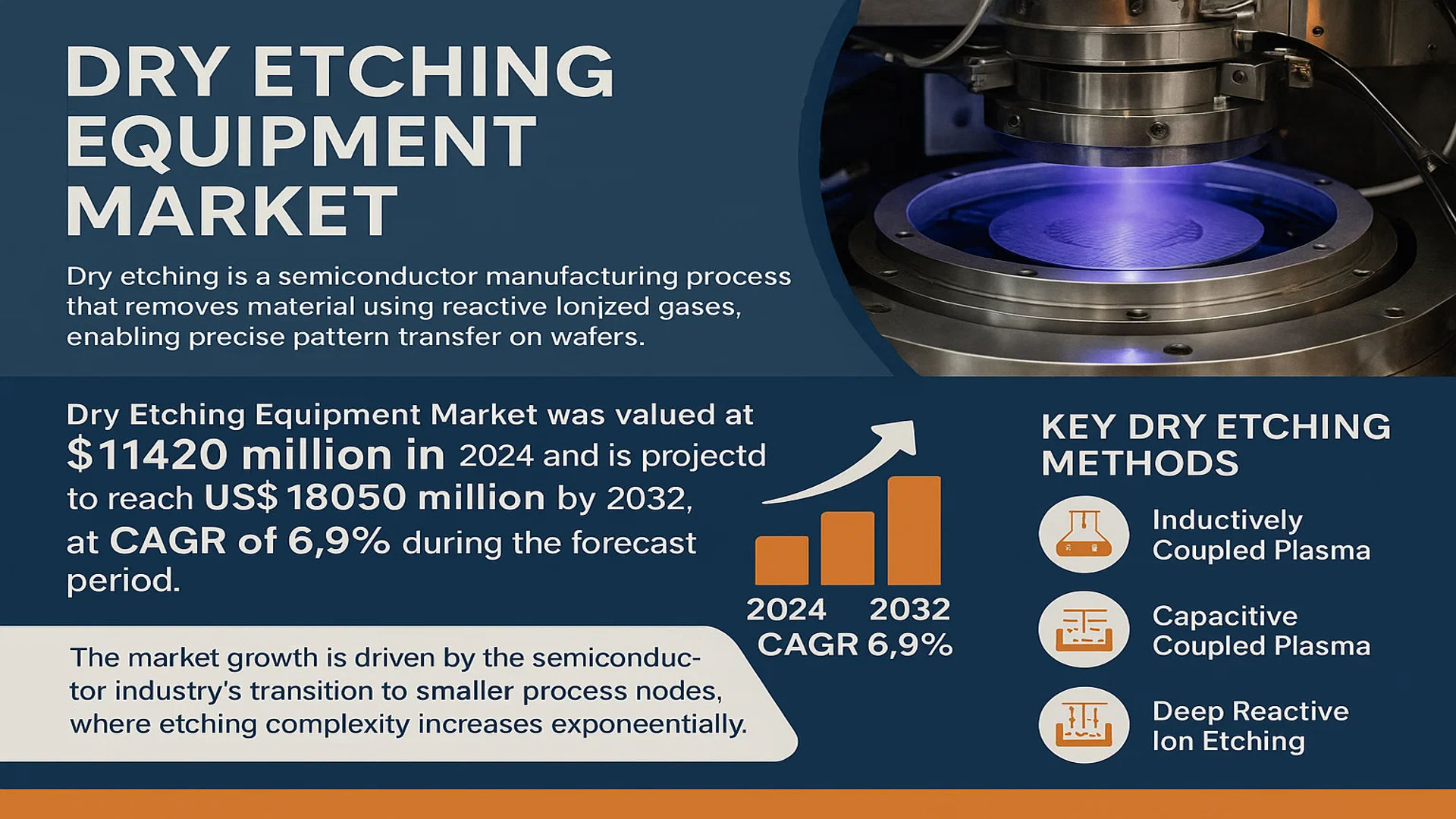
The global Dry Etching Equipment Market was valued at 11420 million in 2024 and is projected to reach US$ 18050 million by 2032, at a CAGR of 6.9% during the forecast period.
Dry etching is a semiconductor manufacturing process that removes material using reactive ionized gases, enabling precise pattern transfer on wafers. This technique is critical for advanced chip fabrication, especially in sub-10nm nodes, as it offers superior anisotropy and selectivity compared to wet etching. Key dry etching methods include Inductively Coupled Plasma (ICP), Capacitive Coupled Plasma (CCP), and Deep Reactive Ion Etching (DRIE), each serving specific applications in logic, memory, and MEMS production.
The market growth is driven by the semiconductor industry’s transition to smaller process nodes, where etching complexity increases exponentially. For instance, 7nm chip production requires 140 etching steps—nearly triple the 40 steps needed for 28nm nodes. Asia-Pacific dominates consumption with 76.07% market share (2024), fueled by massive foundry expansions in Taiwan, South Korea, and China. Leading players like Lam Research, Applied Materials, and Tokyo Electron collectively control over 92% of the global market, though Chinese domestic manufacturers like AMEC are gaining traction with localization initiatives.
MARKET DYNAMICS
MARKET DRIVERS
Expanding Semiconductor Industry to Propel Demand for Dry Etching Equipment
The semiconductor industry’s relentless advancement in process node technologies is a primary driver of the dry etching equipment market. With leading manufacturers transitioning to 3nm and below process nodes, the complexity of etching patterns has increased dramatically. This shift demands highly precise dry etching systems capable of handling intricate designs with minimal defects. In 2024 alone, over 40 new wafer fabrication facilities are under construction globally, with the majority focused on advanced process nodes requiring sophisticated etching solutions. The semiconductor industry’s projected 8% annual growth through 2032 directly translates to increased equipment expenditure, particularly in etching technologies.
3D NAND Memory Expansion Creates Sustained Demand
3D NAND flash memory technology continues its vertical scaling race, with leading manufacturers now producing 200+ layer devices. This architectural evolution directly benefits the dry etching equipment market because stacking additional layers requires increasingly sophisticated high-aspect-ratio etching capabilities. Each new generation of 3D NAND typically requires 20-30% more etch steps than its predecessor, creating a compounding demand for advanced etching systems. The memory sector currently accounts for approximately 35% of all dry etching equipment purchases and is expected to maintain this share as data storage needs grow exponentially across cloud computing and mobile applications.
Government Investments in Domestic Semiconductor Production
National initiatives to strengthen semiconductor supply chains are creating substantial opportunities for dry etching equipment manufacturers. Several regions have introduced substantial incentive programs, with cumulative investments exceeding $200 billion globally for semiconductor fabrication expansion. These projects typically involve installing state-of-the-art equipment capable of producing at the most advanced nodes, where dry etching processes are most critical. The resulting demand for new equipment purchases and technology upgrades presents a significant growth avenue for market players.
MARKET RESTRAINTS
High Equipment Costs Pose Barrier to Market Expansion
The substantial capital expenditure required for advanced dry etching systems acts as a significant market restraint. A single state-of-the-art etching tool can cost between $10-20 million, putting it out of reach for many smaller chip manufacturers and research institutions. This pricing pressure is exacerbated by the increasing complexity of etching processes at advanced nodes, which requires more sophisticated and expensive equipment configurations. While foundries and major IDMs continue investing, the high cost structure limits broader market penetration and slows adoption rates among second-tier manufacturers.
Complexity of Advanced Node Processes Creates Technical Challenges
As semiconductor geometries shrink below 5nm, the technical challenges in etching processes multiply exponentially. Achieving precise pattern transfer while maintaining critical dimension uniformity and defect control requires increasingly complex plasma chemistry and equipment architectures. This complexity introduces yield risks that can negatively impact production volumes and time-to-market. Equipment manufacturers must continually invest in R&D to address these challenges, increasing their cost structure and potentially delaying new product introductions.
Geopolitical Factors Impacting Supply Chains
Recent trade restrictions and technology controls have introduced uncertainty into the dry etching equipment market, particularly for cross-border equipment sales. Export controls affecting advanced semiconductor manufacturing equipment have created bifurcated supply chains, requiring manufacturers to develop separate product roadmaps for different regional markets. These developments increase operational complexity and may slow the pace of technological advancement as companies navigate evolving regulatory landscapes.
MARKET OPPORTUNITIES
Emerging Packaging Technologies Create New Demand
Advanced packaging technologies such as chiplet architectures and 3D IC integration are opening new frontiers for dry etching applications. These packaging approaches require specialized through-silicon via (TSV) etching and wafer thinning processes that differ from conventional front-end etching requirements. As the semiconductor industry increasingly adopts heterogeneous integration strategies, specialized dry etching solutions for packaging applications could represent a $1.5 billion market opportunity by 2030.
AI-Driven Process Optimization Enhances Equipment Value
The integration of artificial intelligence and machine learning into dry etching systems presents significant opportunities for equipment differentiation. Advanced process control systems that can optimize etch parameters in real-time based on incoming wafer measurements can provide substantial improvements in yield and throughput. Several leading equipment manufacturers have already introduced AI-enhanced systems that demonstrate 10-15% improvements in process consistency, creating compelling upgrade opportunities for existing fabrication facilities.
Materials Innovation Expands Application Scope
The development of new semiconductor materials beyond silicon, including compound semiconductors and 2D materials, creates additional demand for specialized dry etching solutions. Each new material system presents unique etching challenges that require tailored plasma chemistries and chamber designs. As these materials move from research to production environments, they represent a growing market segment for equipment manufacturers with specialized capabilities.
DRY ETCHING EQUIPMENT MARKET TRENDS
Increasing Semiconductor Miniaturization Fuels Dry Etching Equipment Demand
The global dry etching equipment market is experiencing significant growth due to the relentless push toward semiconductor miniaturization. As process nodes shrink below 7nm, wafer fabs require more advanced etching solutions to achieve precise feature definition. Modern integrated circuit manufacturing demands over 140 etching steps for 7nm production, compared to just 40 steps for 28nm processes, creating substantial equipment needs. This trend is further amplified by the transition to 3D NAND flash memory, where high aspect ratio etching capabilities become critical for vertical cell stacking. Leading manufacturers are responding with plasma-based etching systems that can achieve aspect ratios exceeding 60:1 while maintaining critical dimension uniformity below 2nm.
Other Trends
Rise of Domestic Manufacturers in Asia-Pacific
While global players like Lam Research and Tokyo Electron dominate the market, regional manufacturers in Asia-Pacific are gaining traction with competitive offerings. Chinese firms such as AMEC and NAURA now capture approximately 12% market share of the APAC etching equipment sector, benefitting from government incentives and localization policies. This shift comes as mainland China accounts for 76% of global dry etching equipment consumption, driven by massive fab construction projects. Local manufacturers have specifically targeted mature process nodes, achieving cost advantages of 15-20% versus imported equipment while maintaining comparable yield performance for 28-45nm applications.
Integration of AI and Advanced Process Control
The industry is witnessing accelerated adoption of artificial intelligence in dry etching systems to optimize process parameters in real-time. Modern etching equipment now incorporates machine learning algorithms that can predict and compensate for chamber drift, reducing wafer scrap rates by up to 40% in high-volume production. This technology convergence enables faster recipe development cycles, with some systems achieving qualified process recipes in 50% less time compared to conventional methods. Furthermore, the integration of IoT-enabled predictive maintenance solutions has extended mean time between failures (MTBF) by 30%, significantly improving fab tool utilization rates.
Expansion into New Application Verticals
While logic and memory applications dominate current demand, dry etching equipment manufacturers are seeing growing opportunities in power devices and advanced packaging. The transition to wide bandgap semiconductors (SiC/GaN) for electric vehicles and renewable energy requires specialized etching capabilities, creating a $1.2 billion addressable market by 2025. Similarly, the rise of heterogeneous integration through chiplet architectures is driving demand for through-silicon via (TSV) etching systems. Equipment vendors are responding with multi-chamber cluster tools that combine etching, deposition, and cleaning capabilities to address these emerging applications.
COMPETITIVE LANDSCAPE
Key Industry Players
Technological Advancements and Strategic Alliances Define Market Competition
The global dry etching equipment market is highly concentrated, with a few dominant players holding significant market share. According to recent industry analysis, the top three manufacturers – Lam Research, Tokyo Electron Limited (TEL), and Applied Materials – collectively control over 92% of the market by revenue. This oligopolistic structure results from the high technical barriers to entry and the extensive R&D investments required to develop advanced etching solutions.
Lam Research maintains its leadership position through continuous innovation in plasma etch technology. The company’s recently introduced Sense.i platform incorporates artificial intelligence for real-time process control, addressing the complex requirements of 3D NAND and advanced logic nodes. Similarly, Tokyo Electron has strengthened its market position through strategic partnerships with leading foundries, particularly in Asia where over 76% of etching equipment is consumed.
Emerging players are challenging this dominance through specialized solutions. AMEC, a Chinese semiconductor equipment manufacturer, has gained traction in the domestic market with its conductor etch systems for 14nm-28nm processes. The company benefits from China’s semiconductor self-sufficiency initiatives, having secured multiple contracts from domestic fabs. Meanwhile, NAURA has expanded its product line to include advanced etching tools for silicon carbide power devices, targeting the growing electric vehicle market.
The competitive intensity is further heightened by vertical integration strategies. Major players are investing heavily in R&D to develop integrated etching solutions that combine multiple process steps. Applied Materials’ recent acquisition of a plasma diagnostics startup exemplifies this trend toward holistic process control systems. Such moves are critical as the industry transitions to sub-5nm nodes where etch precision directly impacts device performance.
List of Key Dry Etching Equipment Companies Profiled
- Lam Research Corporation (U.S.)
- Tokyo Electron Limited (TEL) (Japan)
- Applied Materials, Inc. (U.S.)
- Hitachi High-Technologies Corporation (Japan)
- Oxford Instruments plc (U.K.)
- ULVAC, Inc. (Japan)
- SPTS Technologies (U.K.)
- GigaLane Co., Ltd. (South Korea)
- Plasma-Therm LLC (U.S.)
- SAMCO Inc. (Japan)
- Advanced Micro-Fabrication Equipment Inc. (AMEC) (China)
- NAURA Technology Group Co., Ltd. (China)
Segment Analysis:
By Type
Inductively Coupled Plasma (ICP) Segment Leads Due to Superior Precision in Advanced Node Semiconductor Manufacturing
The market is segmented based on type into:
- Inductively Coupled Plasma (ICP)
- Capacitive Coupled Plasma (CCP)
- Reactive Ion Etching (RIE)
- Deep Reactive Ion Etching (DRIE)
- Others
By Application
Logic and Memory Segment Dominates as Semiconductor Industry Scales Down to 7nm and Below
The market is segmented based on application into:
- Logic and Memory
- MEMS
- Power Device
- Others
By Technology Node
7nm-28nm Segment Shows Strong Demand Due to Increasing Complexity in Chip Manufacturing
The market is segmented based on technology node into:
- <28nm
- 28-14nm
- 14-7nm
- 7-3nm
- Below 3nm
By End User
Foundries Lead the Market as Semiconductor Manufacturing Complexities Increase
The market is segmented based on end user into:
- Foundries
- Integrated Device Manufacturers (IDMs)
- Research Institutions
- Others
Regional Analysis: Dry Etching Equipment Market
Asia-Pacific
The Asia-Pacific region dominates the global dry etching equipment market, accounting for 76.07% of sales revenue in 2019. This leadership stems from massive semiconductor fabrication investments across China, Taiwan, South Korea, and Japan. China alone has become the world’s largest semiconductor equipment market for four consecutive years, with aggressive expansion plans for 28nm-7nm fabs requiring 2.5x more etching steps than previous nodes. Local champions like AMEC and NAURA are gaining traction against global players by offering cost-competitive solutions for mature nodes, while governments actively subsidize domestic equipment development. However, geopolitical tensions and export controls create supply chain uncertainties that may impact regional growth trajectories.
North America
Holding 13% market share, North America remains a critical innovation hub despite production shifts to Asia. The U.S. hosts R&D centers for industry leaders like Lam Research and Applied Materials, who collectively control over 60% of global etching equipment IP. Recent CHIPS Act funding ($52.7 billion) aims to revitalize domestic semiconductor manufacturing, with Intel’s $20 billion Ohio fab project signalling renewed demand for advanced etching systems. The region specializes in cutting-edge applications—particularly for AI/ML chips—where precision etching at 5nm nodes and below commands premium pricing. Regulatory scrutiny on equipment exports to China presents both challenges and opportunities for market repositioning.
Europe
Europe’s market thrives on specialty semiconductor applications, with focus areas including automotive MEMS, power devices, and photonics requiring customized etching solutions. ASML’s EUV leadership indirectly boosts demand for compatible etching systems, particularly in Germany and the Netherlands where equipment suppliers cluster around major research institutions. While the region lags in volume production, EU initiatives like the Chips Act (€43 billion investment) aim to double Europe’s semiconductor market share by 2030. This could benefit equipment manufacturers specializing in heterogeneous integration and 3D IC packaging—processes demanding advanced DRIE (Deep Reactive Ion Etching) capabilities currently supplied primarily by SPTS Technologies and Plasma-Therm.
Middle East & Africa
The emerging MEA market shows potential through strategic partnerships, such as Saudi Arabia’s $6 billion investment in semiconductor materials production which may eventually drive local equipment demand. Israel’s strong fabless design ecosystem creates niche opportunities for MEMS etching systems, but limited local manufacturing infrastructure curtails broader adoption. Recent geopolitical developments, including the Abraham Accords, could facilitate technology transfers that stimulate regional equipment markets over the next decade—though current sales remain negligible at <1% of global totals.
South America
Brazil’s modest but growing aerospace and medical device industries generate steady demand for MEMS-focused etching equipment, primarily imported from U.S. and European suppliers. Argentina’s INVAP has demonstrated capability in specialty semiconductor applications, yet macroeconomic instability hinders capital-intensive equipment investments. The region shows potential as a testing ground for refurbished etching systems redeployed from Asian fabs, though lack of comprehensive semiconductor policies limits market development compared to other emerging economies.
Technology Segmentation Insights
ICP (Inductively Coupled Plasma) systems lead in advanced node applications due to superior ion density control for high-aspect-ratio etching—critical for 3D NAND and FinFET structures. Meanwhile, RIE (Reactive Ion Etching) maintains strong positioning in cost-sensitive MEMS manufacturing where etch precision outweighs throughput requirements. The emergence of atomic layer etching (ALE) promises to reshape competitive dynamics as chipmakers push beyond 3nm node limitations.
Report Scope
This market research report provides a comprehensive analysis of the global Dry Etching Equipment market, covering the forecast period 2025–2032. It offers detailed insights into market dynamics, technological advancements, competitive landscape, and key trends shaping the semiconductor fabrication industry.
Key focus areas of the report include:
- Market Size & Forecast: Historical data and future projections for revenue, unit shipments, and market value across major regions and segments. The global market was valued at USD 11,420 million in 2024 and is projected to reach USD 18,050 million by 2032.
- Segmentation Analysis: Detailed breakdown by product type (ICP, CCP, RIE, DRIE), application (Logic & Memory, MEMS, Power Devices), and end-user industries.
- Regional Outlook: Insights into market performance across North America (13% share), Asia-Pacific (76.07% share), Europe, and other regions, with country-level analysis.
- Competitive Landscape: Profiles of leading participants including Lam Research, Applied Materials, TEL, AMEC and NAURA, covering their market share (top 3 hold 92.16%), R&D focus, and strategic developments.
- Technology Trends: Assessment of advanced etching techniques for 7nm-28nm processes (140 etching steps required for 7nm vs 40 for 28nm), 3D NAND stacking, and high aspect ratio etching.
- Market Drivers: Evaluation of factors including AI/5G/IoT chip demand, China’s semiconductor policy support, and increasing wafer fab projects globally.
- Stakeholder Analysis: Strategic insights for equipment manufacturers, foundries, IDMs, investors, and policymakers in the semiconductor value chain.
The research methodology combines primary interviews with industry experts and comprehensive analysis of verified market data to ensure accuracy and reliability.
FREQUENTLY ASKED QUESTIONS:
What is the current market size of Global Dry Etching Equipment Market?
-> Dry Etching Equipment Market was valued at 11420 million in 2024 and is projected to reach US$ 18050 million by 2032, at a CAGR of 6.9% during the forecast period.
Which key companies operate in Global Dry Etching Equipment Market?
-> Key players include Lam Research, Tokyo Electron (TEL), Applied Materials, Hitachi High-Technologies, AMEC, and NAURA, with the top three holding 92.16% market share.
What are the key growth drivers?
-> Key growth drivers include advancements in semiconductor nodes (7nm-28nm processes), 3D NAND development, and China’s semiconductor self-sufficiency policies.
Which region dominates the market?
-> Asia-Pacific dominates with 76.07% market share, driven by semiconductor manufacturing in China, Taiwan, South Korea and Japan.
What are the emerging trends?
-> Emerging trends include high aspect ratio etching for 3D NAND, atomic layer etching precision, and increasing etching steps for advanced nodes (140 steps for 7nm).

Get Sample Report PDF for Exclusive Insights
Report Sample Includes
- Table of Contents
- List of Tables & Figures
- Charts, Research Methodology, and more...






