Market Insights
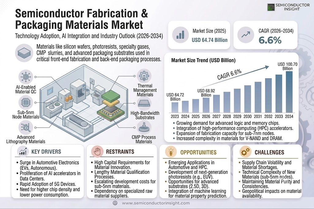
Global Semiconductor Fabrication & Packaging Materials Market size was valued at USD 64.74 billion in 2025. The market is projected to grow from USD 68.92 billion in 2026 to USD 100.70 billion by 2034, exhibiting a CAGR of 6.6% during the forecast period.
Semiconductor fabrication and packaging materials are critical components enabling chip manufacturing and assembly processes. These materials form the foundation for producing integrated circuits (ICs) across front-end wafer fabrication and back-end packaging stages. Key categories include silicon wafers, photoresists, specialty gases for deposition/etching, chemical mechanical planarization (CMP) slurries, lead frames, bonding wires, and advanced substrates like organic laminates or ceramic packages.
The market growth is driven by rising demand for advanced logic/memory chips, expansion of foundry capacity globally, and increasing complexity in packaging technologies such as fan-out wafer-level packaging (FOWLP) and 3D IC stacking. Major players like Shin-Etsu Chemical, SUMCO, DuPont de Nemours Inc., and Resonac Holdings Corporation dominate material supply chains through continuous R&D investments in EUV photoresists, high-purity precursors, and low-dielectric substrates to support sub-5nm node production.
MARKET DRIVERS
Growing Demand for Advanced Semiconductor Devices
Semiconductor Fabrication & Packaging Materials Market is experiencing robust growth driven by increasing demand for advanced semiconductor devices across industries. The proliferation of 5G technology, IoT devices, and AI applications has created unprecedented demand for high-performance chips, requiring specialized fabrication and packaging materials. Foundries are expanding capacity to meet this demand, directly benefiting material suppliers.
Technological Advancements in Packaging Solutions
Innovations in packaging technologies such as 2.5D/3D IC packaging and fan-out wafer-level packaging (FOWLP) are driving material requirements. These advanced packaging solutions require specialized substrates, underfill materials, and thermal interface materials, creating new revenue streams for material providers. The market for advanced packaging materials is growing at approximately 8% annually.
Government initiatives supporting domestic semiconductor production in various regions are further accelerating market growth, with significant investments in fabrication facilities driving material demand.
MARKET CHALLENGES
Supply Chain Volatility and Material Shortages
Semiconductor Fabrication & Packaging Materials Market faces significant challenges from global supply chain disruptions. Critical materials like high-purity silicon wafers, photoresists, and specialty gases have experienced shortages, impacting production schedules. Lead times for certain materials have extended to 6-9 months in some cases, forcing manufacturers to adjust their inventory strategies.
Other Challenges
Technical Complexity of New Materials
Developing and qualifying new materials for next-generation nodes (below 5nm) requires substantial R&D investment and extensive testing cycles, slowing time-to-market for innovative solutions.
MARKET RESTRAINTS
High Capital Requirements for Material Innovation
Semiconductor Fabrication & Packaging Materials Market faces constraints from the substantial investments required for material development and manufacturing. Establishing production facilities for advanced materials like extreme ultraviolet (EUV) photoresists or low-dielectric-constant interconnects can cost hundreds of millions of dollars, limiting market entry for smaller players.
MARKET OPPORTUNITIES
Emerging Applications in Automotive and HPC
The growing adoption of electric vehicles and autonomous driving technologies is creating new opportunities for semiconductor materials. High-performance computing (HPC) applications, including AI accelerators and data center processors, are driving demand for advanced thermal management materials and high-bandwidth packaging solutions.
Semiconductor Fabrication & Packaging Materials Market Trends
Advanced Material Innovations Driving Market Growth
Semiconductor Fabrication & Packaging Materials Market is witnessing significant advancements in material technologies. EUV photoresists, large-size silicon wafers, and high-density packaging substrates are experiencing growing demand as chip manufacturers transition to more advanced nodes. These materials are evolving to meet requirements for lower dielectric constants, higher thermal conductivity, and improved temperature resistance.
Other Trends
Shift Toward Compound Semiconductor Materials
Silicon carbide (SiC) and gallium nitride (GaN) are gaining traction in power electronics and RF applications, creating new opportunities for material suppliers. This diversification is changing the traditional silicon-dominated material landscape while maintaining compatibility with existing fabrication processes.
Geopolitical Factors Impacting Supply Chains
Regional trade policies and export controls are reshaping material sourcing strategies. Asia-Pacific remains the dominant region for semiconductor materials consumption, with China accelerating localization efforts for critical fabrication and packaging materials to reduce supply chain vulnerabilities.
Packaging Material Innovations for Heterogeneous Integration
Advanced packaging technologies like 2.5D/3D ICs and fan-out wafer-level packaging are driving demand for specialized materials. Packaging substrates and underfill materials are evolving to support higher interconnect densities while thermal interface materials are becoming more critical for heat dissipation in complex packages.
Other Trends
Sustainability Initiatives Gaining Importance
Environmental regulations are prompting manufacturers to develop eco-friendly alternatives for packaging resins and fabrication chemicals. This includes reducing hazardous substance content and improving recycling potential while maintaining material performance requirements.
COMPETITIVE LANDSCAPE
Key Industry Players
Innovation and Consolidation Drive Semiconductor Materials Market Competition
Global Semiconductor Fabrication & Packaging Materials Market is dominated by established chemical and material science giants with strong R&D capabilities and global supply chains. Shin-Etsu Chemical leads the silicon wafer segment with over 30% market share, followed by SUMCO and GlobalWafers, forming an oligopolistic structure in this critical substrate market. For advanced packaging materials, Ibiden, Unimicron, and AT&S control nearly 60% of the high-density packaging substrate market, benefiting from their early adoption of flip-chip and fan-out technologies.
Specialty segments feature strong niche players – JSR and TOKYO OHKA KOGYO (TOK) dominate the photoresist market with combined 80% share in EUV photoresists, while Resonac (formerly Showa Denko) leads in high-purity gases. Emerging Chinese players like National Silicon Industry Group (NSIG) and Grinm Advanced Materials are gaining traction in domestic markets through government-supported capacity expansions and technology partnerships. Regional champions like Daeduck Electronics in Korea and Shenzhen Fastprint in China are challenging traditional leaders in mid-tier packaging material segments.
List of Key Semiconductor Fabrication & Packaging Materials Companies Profiled
- Shin-Etsu Chemical
- SUMCO Corporation
- GlobalWafers
- JSR Corporation
- TOKYO OHKA KOGYO (TOK)
- Resonac Holdings
- Ibiden Co., Ltd.
- Unimicron Technology
- AT&S Austria Technologie & Systemtechnik
- Linde plc
- Daeduck Electronics
- National Silicon Industry Group (NSIG)
- Grinm Advanced Materials
- DuPont
- Henkel Electronics
Segment Analysis:
| Segment Category | Sub-Segments | Key Insights |
| By Type |
|
Wafer Fab Materials dominate due to critical role in front-end processes.
|
| By Application |
|
Logic applications show strongest innovation-driven demand:
|
| By End User |
|
Foundries drive material innovation through technical demands:
|
| By Material Technology |
|
Compound Semiconductors show fastest adoption growth:
|
| By Supply Chain Position |
|
Direct Supply to Fabs dominates for critical materials:
|
Regional Analysis: Semiconductor Fabrication & Packaging Materials Market
Asia-Pacific
Taiwan maintains world-leading positions in advanced packaging technologies, driving demand for specialized underfill materials and copper pillar bump solutions. The concentration of OSAT providers creates a dynamic materials innovation ecosystem with strong university-industry collaboration.
Chinese suppliers are rapidly expanding capacity for high-purity process chemicals and photoresists, supported by national semiconductor self-sufficiency goals. Domestic material alternatives are gaining traction in mature nodes while competing through aggressive pricing strategies.
South Korea’s material requirements are shaped by its dominance in memory production, concentrating demand for DRAM packaging substrates and 3D NAND stacking materials. Local conglomerates maintain vertical integration strategies for critical materials procurement.
Japanese chemical companies continue to lead in specialty materials for extreme ultraviolet lithography and wafer-level packaging. Ongoing material science breakthroughs target next-generation heterogenous integration challenges with novel thermally conductive compounds.
North America
North America’s Semiconductor Fabrication & Packaging Materials Market benefits from strong R&D ecosystems and government initiatives like the CHIPS Act. The region specializes in high-value materials for leading-edge logic chips, with particular strengths in EUV photoresists and advanced thermal interface materials. Major IDMs and fabless companies drive demand for packaging materials enabling heterogenous integration. Domestic material suppliers focus on proprietary formulations with performance advantages, while maintaining strict quality control standards expected by North American semiconductor manufacturers.
Europe
Europe maintains a strong position in specialty materials for power electronics and automotive semiconductors, with leading chemical companies supplying high-reliability packaging solutions. The region’s materials innovation focuses on sustainability, with growing emphasis on green chemistry in fabrication processes. Collaborative R&D initiatives between material suppliers and equipment manufacturers target holistic solutions for next-generation semiconductor manufacturing challenges, particularly in the automotive and industrial sectors.
Middle East & Africa
This emerging region is witnessing increased investments in semiconductor material supply chains, particularly for packaging substrates and basic process chemicals. Government initiatives aim to develop local material production capabilities to support regional electronics manufacturing growth. Strategic partnerships with established material suppliers from Asia and Europe are accelerating technology transfer while addressing specific regional requirements for harsh environment applications.
South America
South America’s Semiconductor Fabrication & Packaging Materials Market remains comparatively small but shows growth potential in supporting regional electronics assembly. Local material production focuses primarily on basic packaging components, with increasing foreign investment in high-purity chemical plants. The region serves as a strategic location for material suppliers looking to diversify global supply chains while serving growing domestic semiconductor packaging demand.
Report Scope
This market research report provides a comprehensive analysis of the Semiconductor Fabrication & Packaging Materials Market, covering the forecast period 2025–2034. It offers detailed insights into market dynamics, technological advancements, competitive landscape, and key trends shaping the industry.
Key focus areas of the report include:
- Market Overview: The report begins with an overview outlining its current market scenario, key growth indicators, and industry transformation drivers. It discusses macroeconomic factors, demand–supply balance, regulatory landscape, and the strategic role of semiconductors in powering advancements across industries such as automotive, telecommunications, consumer electronics, and industrial automation.
- Market Size & Forecast: Historical data and future projections for revenue, unit shipments, and market value across major regions and segments.
- Segmentation Analysis: Detailed breakdown by product type, technology, application, and end-user industry to identify high-growth segments and investment opportunities.
- Regional Insights: Insights into market performance across North America, Europe, Asia-Pacific, Latin America, and the Middle East & Africa, including country-level analysis where relevant.
- Competitive Landscape: Profiles of leading market participants, including their product offerings, R&D focus, manufacturing capacity, pricing strategies, and recent developments such as mergers, acquisitions, and partnerships.
- Technology Trends & Innovation: Assessment of emerging technologies, integration of AI/IoT, semiconductor design trends, fabrication techniques, and evolving industry standards.
- Market Drivers & Restraints: Evaluation of factors driving market growth along with challenges, supply chain constraints, regulatory issues, and market-entry barriers.
- Stakeholder Insights: Insights for component suppliers, OEMs, system integrators, investors, and policymakers regarding the evolving ecosystem and strategic opportunities.
Primary and secondary research methods are employed, including interviews with industry experts, data from verified sources, and real-time market intelligence to ensure the accuracy and reliability of the insights presented.
FREQUENTLY ASKED QUESTIONS:
What is the current market size of Semiconductor Fabrication & Packaging Materials Market?
-> Semiconductor Fabrication & Packaging Materials Market size was valued at USD 64.74 billion in 2025. The market is projected to grow from USD 68.92 billion in 2026 to USD 100.70 billion by 2034, exhibiting a CAGR of 6.6% during the forecast period.
Which key companies operate in Semiconductor Fabrication & Packaging Materials Market?
-> Key players include Shin-Etsu Chemical, SUMCO, Siltronic AG, Resonac, DuPont, Fujifilm, Merck, Henkel, KYOCERA, and Shinko Electric Industries, among others.
What are the key growth drivers?
-> Key growth drivers include advancements in semiconductor manufacturing processes, increasing demand for electronics, rising adoption of AI/IoT technologies, and expansion of 5G infrastructure.
Which region dominates the market?
-> Asia-Pacific dominates the market, with Taiwan China, Mainland China, Japan and South Korea forming core industrial clusters.
What are the emerging trends?
-> Emerging trends include adoption of third-generation semiconductor materials (SiC/GaN), development of EUV-compatible materials, and shift toward advanced packaging solutions.
Get Sample Report PDF for Exclusive Insights
Report Sample Includes
- Table of Contents
- List of Tables & Figures
- Charts, Research Methodology, and more...
 Download Sample Report PDF