3D NAND (200+, 300+ Layer) Market Insights
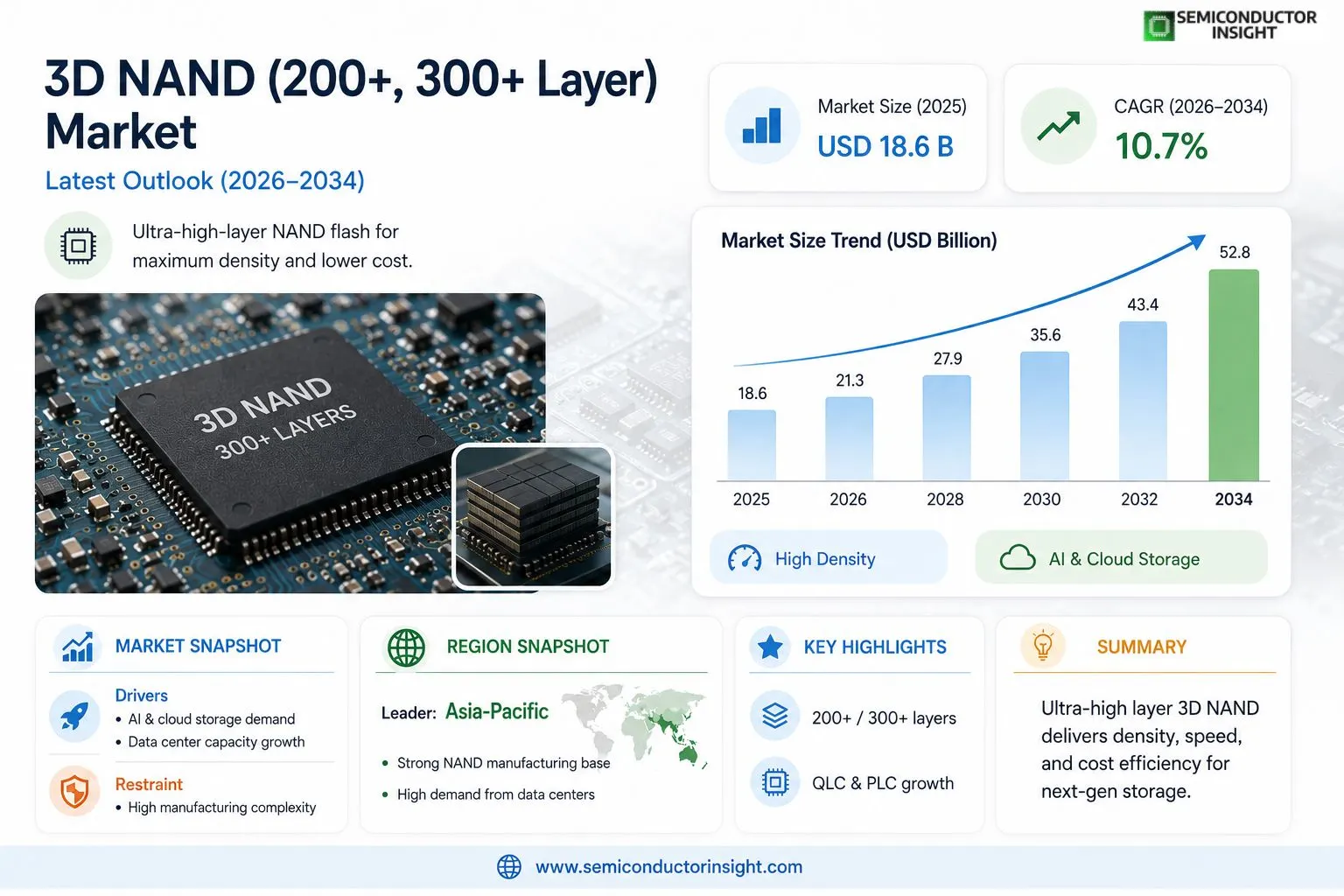
Global 3D NAND (200+, 300+ Layer) market size was valued at USD 18.6 billion in 2025. The market is projected to grow from USD 21.3 billion in 2026 to USD 52.8 billion by 2034, exhibiting a CAGR of 10.7% during the forecast period.
3D NAND flash memory with 200+ and 300+ layers represents the most advanced tier of non-volatile storage technology, engineered by vertically stacking memory cells to dramatically increase storage density while reducing the per-bit cost. Unlike planar NAND, these ultra-high-layer configurations enable manufacturers to achieve significantly greater bit density per unit area, making them foundational to modern solid-state drives (SSDs), smartphones, enterprise storage arrays, and data center infrastructure. Key product categories within this segment include TLC (Triple-Level Cell), QLC (Quad-Level Cell), and PLC (Penta-Level Cell) NAND architectures built on 200-layer-and-above process nodes.
The market is experiencing robust growth driven by surging demand for high-capacity storage in artificial intelligence workloads, cloud computing infrastructure, and consumer electronics. Furthermore, the rapid proliferation of generative AI applications is compelling hyperscale data center operators to deploy increasingly dense storage solutions. Leading manufacturers are actively advancing their layer counts — for instance, Samsung has introduced 290-layer V-NAND, while Micron has commenced volume production of its 232-layer NAND, and SK Hynix has announced development of 321-layer NAND technology. Samsung Electronics, Micron Technology, SK Hynix, Kioxia, and Western Digital are among the key players shaping this market with expansive and competitive product portfolios.
MARKET DRIVERS
Surging Demand for High-Density Storage in Data Centers and Cloud Infrastructure
3D NAND (200+, 300+ Layer) Market is experiencing robust growth momentum driven primarily by the exponential rise in data generation across enterprise, hyperscale, and edge computing environments. As cloud service providers continue to expand their infrastructure to accommodate AI workloads, machine learning pipelines, and real-time analytics, the need for high-capacity, energy-efficient solid-state storage has intensified significantly. Advanced-layer 3D NAND technologies, particularly those exceeding 200 and 300 layers, offer substantially improved bit density per die, enabling manufacturers to deliver higher storage capacities while reducing cost-per-gigabyte — a critical metric for large-scale data center deployments.
AI, Machine Learning, and Generative AI Workloads Accelerating NAND Adoption
The proliferation of generative AI platforms and large language model (LLM) training has created an unprecedented demand for fast, high-endurance NAND flash storage. Training and inference operations associated with AI models require high-throughput storage solutions capable of sustaining intensive read/write cycles, which makes high-layer-count 3D NAND an ideal candidate. 3D NAND (200+, 300+ Layer) Market is directly benefiting from increased capital expenditure by technology companies investing in AI infrastructure, as next-generation NAND with 200+ and 300+ layer stacks provides the performance characteristics necessary for these demanding computational environments.
➤ Leading NAND manufacturers including Samsung, SK Hynix, Micron, Kioxia, and Western Digital have publicly announced and begun mass production or qualification of 200+ and 300+ layer 3D NAND products, signaling a decisive industry-wide transition toward ultra-high-layer-count architectures as the new standard for next-generation storage solutions.
Consumer electronics continue to serve as a significant volume driver for 3D NAND (200+, 300+ Layer) Market, with smartphones, laptops, and tablets increasingly adopting higher-capacity NAND flash to meet user expectations for faster app loading, seamless multitasking, and expanded local storage. The transition toward UFS 4.0 and PCIe Gen 5-based NVMe interfaces in premium consumer devices is further incentivizing OEMs to source advanced-layer NAND that can sustain the bandwidth demands of these next-generation interfaces, reinforcing the market’s upward trajectory.
MARKET CHALLENGES
Engineering Complexity and Yield Management in Ultra-High-Layer-Count 3D NAND Fabrication
One of the most significant challenges confronting 3D NAND (200+, 300+ Layer) Market is the extraordinary engineering complexity associated with stacking memory cells beyond 200 and 300 layers. As layer counts increase, manufacturers face heightened difficulties related to etch depth uniformity, channel hole aspect ratios, and stress-induced wafer deformation. These physical constraints directly impact production yields, and even marginal yield degradation at scale can translate into substantial revenue losses. The transition from sub-200-layer to 200+ and 300+ layer architectures demands significant re-engineering of existing process flows, often requiring entirely new tooling investments and extended qualification timelines before volume production can begin.
Other Challenges
Escalating Capital Expenditure Requirements
Developing and scaling 200+ and 300+ layer 3D NAND manufacturing nodes requires substantial capital investment in advanced lithography equipment, atomic layer deposition tools, and precision metrology systems. For smaller or emerging NAND manufacturers, these financial barriers can limit competitive participation in the high-layer-count segment, potentially consolidating market power among a handful of well-capitalized incumbents.
Thermal Management and Reliability Concerns
As 3D NAND stacks grow taller, heat dissipation within the memory die becomes increasingly difficult to manage. Elevated operating temperatures in ultra-high-layer configurations can accelerate charge leakage and reduce data retention characteristics over time. Ensuring that 200+ and 300+ layer NAND products meet the reliability and endurance standards required for enterprise SSD applications remains an active engineering challenge for all participants in 3D NAND (200+, 300+ Layer) Market.
Supply-Demand Volatility and Pricing Cyclicality
The NAND flash industry is historically susceptible to pronounced boom-and-bust pricing cycles driven by capacity additions outpacing demand growth. The aggressive ramp of 200+ and 300+ layer capacity by multiple manufacturers simultaneously introduces the risk of oversupply conditions, which can compress average selling prices and erode manufacturer profitability, making long-term investment planning difficult for suppliers and buyers alike.
MARKET RESTRAINTS
Geopolitical Tensions and Export Control Regulations Constraining Global Supply Chains
3D NAND (200+, 300+ Layer) Market faces meaningful restraints stemming from evolving geopolitical dynamics, particularly restrictions on semiconductor equipment exports to certain regions. Regulatory actions limiting the transfer of advanced lithography and deposition tools have the potential to significantly impair the ability of affected manufacturers to develop and scale ultra-high-layer-count NAND processes. These constraints introduce supply chain uncertainty and may alter the competitive landscape by limiting the pace at which certain producers can bring 200+ and 300+ layer technologies to market, thereby affecting global pricing, availability, and technology diffusion timelines.
Technological Transition Risks and Legacy Infrastructure Compatibility Barriers
A tangible restraint on the broader adoption of 200+ and 300+ layer 3D NAND is the compatibility challenge associated with transitioning existing storage controller ecosystems and firmware stacks to support the electrical and timing characteristics of next-generation NAND dies. Enterprise storage system integrators must invest in validation and qualification cycles before deploying new NAND generations, creating a lag between product availability and widespread market penetration. Additionally, customers with large installed bases of legacy storage infrastructure may defer upgrades, slowing the revenue realization curve for advanced-layer NAND products in certain end-market segments of 3D NAND (200+, 300+ Layer) Market.
The competitive pressure from emerging alternative storage technologies, including Storage Class Memory (SCM) solutions and advances in computational storage, represents an incremental restraint on the long-term total addressable market for ultra-high-layer NAND in performance-critical applications. While 3D NAND retains compelling cost and density advantages over competing non-volatile memory technologies, the continued maturation of alternatives warrants consideration as a factor that could limit the addressable share of certain high-value application segments over a multi-year horizon.
MARKET OPPORTUNITIES
Expanding Automotive and Industrial Applications Creating New Demand Verticals
3D NAND (200+, 300+ Layer) Market stands to benefit substantially from the accelerating digitization of automotive platforms, including advanced driver-assistance systems (ADAS), in-vehicle infotainment, and the data logging requirements of autonomous vehicle development programs. These applications demand storage solutions combining high capacity, wide operating temperature ranges, and robust endurance — characteristics that advanced-layer 3D NAND is increasingly engineered to deliver. As automotive-grade NAND qualifications for 200+ layer products progress across leading suppliers, the automotive vertical is poised to become a meaningful incremental demand source beyond the traditional consumer and enterprise segments.
Next-Generation QLC and PLC Architectures Unlocking Superior Cost-Per-Bit Economics
The combination of ultra-high layer counts with Quad-Level Cell (QLC) and emerging Penta-Level Cell (PLC) cell architectures presents a compelling opportunity to dramatically reduce the cost-per-gigabyte of NAND flash storage, expanding the addressable market into price-sensitive applications currently served by hard disk drives. As 200+ and 300+ layer QLC NAND matures in terms of endurance and controller optimization, 3D NAND (200+, 300+ Layer) Market has a clear pathway to displace HDDs in near-line storage and warm-storage applications within hyperscale data centers, representing one of the largest volume displacement opportunities in the broader storage industry.
The rapid build-out of 5G network infrastructure globally is generating significant opportunity for 3D NAND (200+, 300+ Layer) Market, as base station equipment, mobile edge computing nodes, and network function virtualization platforms all require compact, high-capacity, and power-efficient flash storage solutions. Ultra-high-layer-count 3D NAND, with its favorable density and power consumption profile relative to earlier-generation NAND, is well-positioned to capture design wins in these infrastructure deployments. Furthermore, the ongoing expansion of national digital infrastructure initiatives across emerging economies represents an additional long-term demand catalyst that could sustain elevated NAND consumption well beyond current forecast horizons.
3D NAND (200+, 300+ Layer) Market Trends
Accelerating Layer Counts Redefining Storage Density Benchmarks
3D NAND (200+, 300+ Layer) Market is witnessing a pivotal technological shift as leading manufacturers aggressively push vertical stacking capabilities to unprecedented heights. Samsung Electronics has introduced its 290-layer V-NAND, Micron Technology has commenced volume production of 232-layer NAND, and SK Hynix has announced development of 321-layer NAND technology. These advances are fundamentally redefining storage density benchmarks across the industry, enabling higher bit density per unit area while progressively reducing per-bit cost — two outcomes that are simultaneously accelerating adoption across enterprise, consumer, and hyperscale segments.
Other Trends
Generative AI and Hyperscale Data Centers Driving Dense Storage Demand
The rapid proliferation of generative AI applications is compelling hyperscale data center operators to deploy increasingly dense storage solutions. AI workloads require high-throughput, low-latency storage infrastructure, and 3D NAND flash memory with 200+ and 300+ layer configurations has emerged as the foundational technology meeting these requirements. Cloud computing operators are scaling their infrastructure investments significantly, creating sustained demand for advanced NAND architectures built on ultra-high-layer process nodes.
Transition from TLC to QLC and PLC Architectures
Within 3D NAND (200+, 300+ Layer) Market, a notable architectural transition is underway. While Triple-Level Cell (TLC) NAND has historically dominated volume deployments, Quad-Level Cell (QLC) and emerging Penta-Level Cell (PLC) configurations are gaining traction as manufacturers seek to maximize storage capacity per die. This shift enables greater cost efficiency for read-intensive workloads such as cloud storage and content delivery, broadening the addressable use cases for ultra-high-layer NAND technology.
Consumer Electronics and SSD Adoption Sustaining Market Momentum
Beyond data centers, 3D NAND (200+, 300+ Layer) Market continues to benefit from robust demand in consumer electronics and solid-state drives. Smartphones, laptops, and portable devices are incorporating higher-capacity NAND storage as user expectations for performance and storage expand. Solid-state drives leveraging 200+ layer NAND are increasingly displacing legacy storage in both consumer and enterprise environments, supported by the competitive product portfolios of key players including Samsung Electronics, Micron Technology, SK Hynix, Kioxia, and Western Digital. This broad demand diversification is reinforcing long-term growth sustainability across 3D NAND (200+, 300+ Layer) Market landscape.
COMPETITIVE LANDSCAPE
Key Industry Players
3D NAND (200+, 300+ Layer) Market: Competitive Dynamics and Leading Manufacturers Shaping the Future of Ultra-High-Density Flash Storage
Global 3D NAND (200+, 300+ Layer) market is characterized by intense technological competition among a concentrated group of semiconductor giants, each racing to achieve higher layer counts, improved bit density, and lower cost-per-gigabyte economics. Samsung Electronics maintains its dominant position as the world’s largest NAND flash supplier, having introduced its 290-layer V-NAND architecture that leverages advanced cell-stacking techniques to deliver industry-leading storage density for enterprise SSDs and consumer devices. Micron Technology has also emerged as a key frontrunner, having commenced volume production of its 232-layer NAND and actively developing subsequent-generation nodes to serve the rapidly expanding AI infrastructure and data center storage segments. SK Hynix has announced development of 321-layer NAND technology, signaling the industry’s aggressive trajectory toward the 300+ layer threshold. Kioxia (formerly Toshiba Memory) and its longstanding joint-venture partner Western Digital continue to co-develop and mass-produce competitive high-layer BiCS NAND solutions, maintaining a strong dual-brand presence across enterprise and client SSD markets. The competitive intensity is further amplified by surging demand from hyperscale cloud operators and generative AI workloads, compelling all major players to accelerate capital expenditure and process node advancement in parallel.
Beyond the established leaders, several other players contribute meaningfully to the 3D NAND (200+, 300+ Layer) ecosystem. China-based YMTC (Yangtze Memory Technologies Co.) has made notable strides with its proprietary Xtacking architecture, enabling competitive layer stacking efficiencies and positioning the company as a significant emerging force in both domestic and select international markets. Intel’s NAND business, divested to SK Hynix, has been integrated into the latter’s expanding product portfolio, further consolidating SK Hynix’s competitive standing. Downstream SSD solution providers such as Seagate Technology, Kingston Technology, and Sabrent leverage NAND wafers from primary manufacturers to offer differentiated storage products across consumer, prosumer, and enterprise segments. System integrators and module makers including Crucial (Micron’s consumer brand) and SanDisk (Western Digital’s consumer brand) extend the market reach of their parent companies’ advanced NAND nodes. The collective competitive landscape is thus defined by a combination of vertically integrated memory manufacturers and agile downstream solution providers, all operating within a high-capital, IP-intensive environment where layer-count leadership directly translates to market share advantage.
List of Key 3D NAND (200+, 300+ Layer) Companies Profiled
- Samsung Electronics Co., Ltd.
- Micron Technology, Inc.
- SK Hynix Inc.
- Kioxia Holdings Corporation
- Western Digital Corporation
- Yangtze Memory Technologies Co., Ltd. (YMTC)
- Seagate Technology Holdings plc
- Kingston Technology Company, Inc.
- Sabrent
- Crucial (Micron Consumer Products Group)
- SanDisk (Western Digital Consumer Brand)
- Phison Electronics Corporation
- Silicon Motion Technology Corporation
Segment Analysis:
| Segment Category | Sub-Segments | Key Insights |
| By Type |
|
TLC (Triple-Level Cell) NAND continues to hold a commanding position in the 3D NAND 200+ and 300+ layer market, owing to its well-established balance between performance, endurance, and storage density.
|
| By Application |
|
Solid-State Drives (SSDs) represent the dominant application segment within the 3D NAND 200+ and 300+ layer market, underpinned by the accelerating transition from traditional hard disk drives across consumer, commercial, and enterprise environments.
|
| By End User |
|
Hyperscale Data Center Operators stand out as the most strategically significant end user category, as the exponential growth of cloud-native services, AI model hosting, and real-time analytics places enormous pressure on storage infrastructure to deliver higher density, lower power consumption, and improved cost efficiency.
|
| By Layer Count |
|
200–249 Layer NAND currently anchors volume production across the industry, with manufacturers such as Micron having scaled 232-layer NAND to high-volume commercial output, making it the most accessible ultra-high-layer configuration in the near term.
|
| By Interface Technology |
|
NVMe (Non-Volatile Memory Express) is the overwhelmingly preferred interface for next-generation 3D NAND deployments, particularly in enterprise and data center environments where the protocol’s ability to exploit the low-latency and high-throughput characteristics of advanced flash is indispensable.
|
Regional Analysis: 3D NAND (200+, 300+ Layer) Market
Asia-Pacific
South Korea anchors the Asia-Pacific 3D NAND (200+, 300+ Layer) landscape through relentless layer-scaling investment and advanced process node development. Leading manufacturers headquartered here are aggressively transitioning production lines toward 300+ layer architectures, targeting enterprise SSDs, hyperscale cloud infrastructure, and next-generation mobile platforms. Government semiconductor roadmaps provide long-term policy stability that encourages multi-year capital commitments to NAND technology advancement.
China is accelerating indigenous 3D NAND (200+, 300+ Layer) production capacity at a pace few anticipated, supported by substantial state-directed funding and a clear policy mandate for semiconductor independence. Domestic players are closing the technological gap in high-layer NAND design, targeting local data center and consumer device markets first before eyeing broader export opportunities. Regulatory dynamics and technology access challenges continue to shape the pace of advancement.
Japan’s role in the Asia-Pacific 3D NAND (200+, 300+ Layer) market is uniquely positioned around the supply of critical materials, precision semiconductor equipment, and specialized chemicals essential for ultra-high-layer fabrication. Japanese suppliers exert significant influence over global NAND production timelines, as advancements in deposition, etching, and inspection technologies frequently originate from this ecosystem. Strategic alliances between Japanese equipment firms and global chipmakers continue to deepen.
Emerging economies within Southeast Asia are increasingly attracting back-end semiconductor assembly and testing operations linked to the 3D NAND (200+, 300+ Layer) value chain. Countries such as Vietnam, Malaysia, and Thailand are benefiting from supply chain diversification strategies adopted by global chipmakers, positioning ASEAN as a growing node in the broader Asia-Pacific NAND ecosystem. Infrastructure investments and skilled workforce development programs are accelerating regional readiness.
North America
North America represents a critically strategic region in 3D NAND (200+, 300+ Layer) Market, characterized by its dominant position as the world’s largest consumer of advanced NAND flash storage across hyperscale data centers, cloud computing platforms, and enterprise IT infrastructure. The United States houses the headquarters of leading cloud service providers and technology conglomerates whose insatiable demand for high-density, high-performance storage solutions directly shapes global 3D NAND technology roadmaps. Recent legislative efforts aimed at reshoring semiconductor manufacturing have begun catalyzing domestic NAND fabrication investments, with new facility announcements signaling a long-term shift toward reducing import dependency. The region also benefits from world-class research universities, national laboratories, and semiconductor design firms that contribute foundational innovations in memory architecture. Canada supports the ecosystem through advanced materials research and a growing pool of semiconductor engineering talent. North America’s regulatory environment, intellectual property frameworks, and defense-driven demand for secure, domestically produced memory solutions further distinguish its role in the evolving 3D NAND (200+, 300+ Layer) global landscape.
Europe
Europe occupies a distinct and increasingly proactive position in 3D NAND (200+, 300+ Layer) Market, driven by the European Union’s strategic imperative to reduce dependence on Asian semiconductor supply chains. While Europe has historically been a consumer rather than a producer of advanced NAND flash memory, significant policy initiatives are reshaping this dynamic by incentivizing semiconductor manufacturing investment across member states. Countries such as Germany, France, and the Netherlands are emerging as focal points for semiconductor ecosystem development, supported by the European Chips Act and complementary national industrial strategies. European demand for 3D NAND (200+, 300+ Layer) technology is substantial, particularly from automotive electronics, industrial automation, telecommunications infrastructure, and enterprise storage sectors. The region’s stringent data sovereignty regulations and growing emphasis on secure digital infrastructure are also fostering demand for locally sourced or allied-nation-produced memory solutions. European semiconductor equipment manufacturers, particularly in the lithography and metrology segments, continue to play indispensable roles in enabling global 3D NAND layer-scaling advancements.
United States
The United States commands an outsized influence over 3D NAND (200+, 300+ Layer) Market relative to its current domestic production footprint, functioning as the primary demand engine, technology innovator, and geopolitical architect of global semiconductor trade policy. American hyperscale cloud operators, enterprise storage vendors, and consumer electronics brands collectively constitute one of the largest end-user bases for advanced NAND flash storage worldwide. The CHIPS and Science Act has injected renewed momentum into domestic memory manufacturing ambitions, encouraging meaningful capital allocation toward next-generation NAND fabrication facilities on American soil. U.S.-based semiconductor design firms are also pioneering controller architectures and interface standards optimized specifically for 200+ and 300+ layer 3D NAND devices. Export control policies enacted by U.S. authorities have introduced new complexities into Global supply chain, influencing technology transfer decisions, equipment sales, and competitive positioning across the international 3D NAND (200+, 300+ Layer) market landscape through the forecast horizon.
Middle East & Africa
The Middle East and Africa region represents an emerging frontier in 3D NAND (200+, 300+ Layer) Market, currently driven predominantly by consumption demand rather than indigenous manufacturing capacity. Rapid digital transformation initiatives across Gulf Cooperation Council nations, including ambitious smart city projects, sovereign cloud infrastructure deployments, and expanding mobile broadband networks, are generating growing appetites for high-density NAND flash storage solutions. The United Arab Emirates and Saudi Arabia are investing heavily in data center construction, creating sustained downstream demand for advanced memory technologies. Africa’s contribution, while nascent, is gaining momentum as mobile internet penetration deepens and fintech adoption accelerates across key economies such as Nigeria, Kenya, and South Africa. The region’s strategic importance to global 3D NAND (200+, 300+ Layer) market participants is expected to grow progressively as digital infrastructure matures, sovereign data policies evolve, and regional technology investment ecosystems develop sufficient scale to attract broader supply chain engagement from leading memory manufacturers and distributors.
Report Scope
This market research report provides a comprehensive analysis of the 3D NAND (200+, 300+ Layer) Market , covering the forecast period 2026–2034. It offers detailed insights into market dynamics, technological advancements, competitive landscape, and key trends shaping the industry.
Key focus areas of the report include:
- Market Overview: The report begins with an overview outlining its current market scenario, key growth indicators, and industry transformation drivers. It discusses macroeconomic factors, demand–supply balance, regulatory landscape, and the strategic role of semiconductors in powering advancements across industries such as automotive, telecommunications, consumer electronics, and industrial automation.
- Market Size & Forecast: Historical data and future projections for revenue, unit shipments, and market value across major regions and segments.
- Segmentation Analysis: Detailed breakdown by product type, technology, application, and end-user industry to identify high-growth segments and investment opportunities.
- Regional Insights: Insights into market performance across North America, Europe, Asia-Pacific, Latin America, and the Middle East & Africa, including country-level analysis where relevant.
- Competitive Landscape: Profiles of leading market participants, including their product offerings, R&D focus, manufacturing capacity, pricing strategies, and recent developments such as mergers, acquisitions, and partnerships.
- Technology Trends & Innovation: Assessment of emerging technologies, integration of AI/IoT, semiconductor design trends, fabrication techniques, and evolving industry standards.
- Market Drivers & Restraints: Evaluation of factors driving market growth along with challenges, supply chain constraints, regulatory issues, and market-entry barriers.
- Stakeholder Insights: Insights for component suppliers, OEMs, system integrators, investors, and policymakers regarding the evolving ecosystem and strategic opportunities.
Primary and secondary research methods are employed, including interviews with industry experts, data from verified sources, and real-time market intelligence to ensure the accuracy and reliability of the insights presented.
FREQUENTLY ASKED QUESTIONS:
What is the current market size of 3D NAND (200+, 300+ Layer) Market?
-> Global 3D NAND (200+, 300+ Layer) Market was valued at USD 18.6 billion in 2025 and is projected to grow from USD 21.3 billion in 2026 to USD 52.8 billion by 2034, exhibiting a CAGR of 10.7% during the forecast period.
Which key companies operate in 3D NAND (200+, 300+ Layer) Market?
-> Key players include Samsung Electronics, Micron Technology, SK Hynix, Kioxia, and Western Digital, among others.
What are the key growth drivers?
-> Key growth drivers include surging demand for high-capacity storage in artificial intelligence workloads, cloud computing infrastructure, and consumer electronics, as well as the rapid proliferation of generative AI applications compelling hyperscale data center operators to deploy increasingly dense storage solutions.
Which region dominates the market?
-> Asia-Pacific is a dominant region in 3D NAND (200+, 300+ Layer) Market, driven by the presence of leading manufacturers such as Samsung Electronics, SK Hynix, and Kioxia, along with strong demand from consumer electronics and data center industries.
What are the emerging trends?
-> Emerging trends include advancement to ultra-high layer counts such as Samsung’s 290-layer V-NAND, Micron’s 232-layer NAND in volume production, and SK Hynix’s announced 321-layer NAND technology, alongside growing adoption of QLC and PLC NAND architectures to maximize storage density and reduce per-bit cost.

Get Sample Report PDF for Exclusive Insights
Report Sample Includes
- Table of Contents
- List of Tables & Figures
- Charts, Research Methodology, and more...