Key Statistics
Key Takeaways
- Type leadership is internally inconsistent on the source page. The detailed segment table says Thin Film Lithium Niobate Phase Modulators dominate because of coherent and quantum applications, while the trends section separately states intensity modulators hold 55% share. The HTML preserves both product types but does not invent a reconciled share.
- Optical Communication is the dominant application, with the source page assigning it more than 65% share and linking demand to 400G/800G/1.6T transceivers, coherent transmission and hyperscale data-center interconnects. Fiber-optic gyroscopes, quantum technologies and LiDAR create smaller but technically differentiated demand.
- North America leads high-end deployments according to both the FAQ and detailed regional narrative, while Asia Pacific is the fastest-growing manufacturing region. The source page assigns the United States 75% of North America, although that figure is treated as source-page evidence rather than independently verified.
- High-volume manufacturing became materially more credible in 2026. HyperLight, UMC and Wavetek announced 6-inch and 8-inch foundry production of the TFLN Chiplet platform in March, moving the technology beyond small-volume photonics fabrication toward a CMOS-fab-style manufacturing model.
- The source-page CAGR does not reconcile with the size anchors. USD 51.1 million in 2024 and USD 722 million in 2032 imply approximately 39.2% CAGR, not the printed 44.4%, producing rebased values of about USD 71.2 million in 2025, USD 99.1 million in 2026 and USD 1.40 billion in 2034.
Thin Film Lithium Niobate (TFLN) Modulator Market Overview
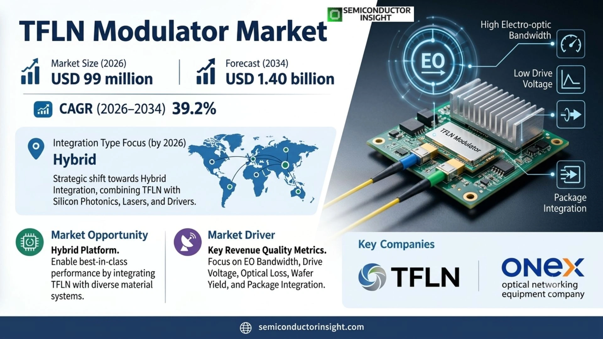
Thin Film Lithium Niobate (TFLN) Modulator market is valued at USD 71 million in 2025, increases to an estimated USD 99 million in 2026, and is projected to reach USD 1.40 billion by 2034. The selected source-page size anchors imply a 39.2% CAGR during 2026–2034. North America is the largest high-end deployment market in 2025 because the source-page FAQ and detailed regional section both place North America in the lead while Asia Pacific is described as the fastest-growing manufacturing hub, while current demand is being reshaped by 400G-per-lane and 1.6T/3.2T optical links, coherent transmission above 100 GBaud, AI data-center power constraints, high-volume 6-inch and 8-inch TFLN foundry production, hybrid silicon-photonics integration, quantum photonics and increasingly integrated optical-engine architectures.
Thin-film lithium niobate modulators exploit the strong Pockels electro-optic effect of lithium niobate in a wafer-scale photonic platform, enabling low-loss waveguides, high electro-optic bandwidth and lower drive voltage than traditional bulk lithium-niobate devices. In practical systems, the modulator converts an electrical data or phase signal into controlled optical amplitude or phase. TFLN is especially attractive where bandwidth, linearity, optical loss and power consumption must be optimized simultaneously rather than traded against one another.
Commercialization accelerated in 2026 because the industry began connecting TFLN device performance with scalable semiconductor manufacturing. HyperLight, UMC and Wavetek announced high-volume production on both 6-inch and 8-inch wafers, while HyperLight’s current platform targets 400G per lane, coherent transmission and co-packaged optics. AFR’s product platform similarly spans 4-inch and 6-inch TFLN fabrication, 130 GBaud coherent driver modulators and PAM-4 chips extending toward 400G per lane. These developments support a transition from laboratory PIC demonstrations toward repeatable production.
Application economics are strongest in optical communication because AI clusters and telecom systems value both bandwidth and reduced electrical drive power. The source page states optical communication represents more than 65% of the market. Quantum and sensing applications are smaller but benefit from the same low optical loss, phase stability and broadband electro-optic response. The technology is therefore unusual in serving very high-volume datacom ambitions and specialized scientific markets from a common material platform.
Segment Analysis: By Type
The source page segments the market into Thin Film Lithium Niobate Phase Modulator and Thin Film Lithium Niobate Intensity Modulator. It contains a direct inconsistency: the segment table says phase modulators dominate, while the trends section assigns intensity modulators 55% share and phase modulators 45%. Both source statements are preserved in the narrative, and no unsupported reconciled share is created.
| Type | Technical / commercial role | Market position |
|---|---|---|
| Thin Film Lithium Niobate Phase Modulator | Phase modulators vary the optical phase without intentionally changing amplitude and are used in coherent communications, frequency-comb generation, sensing and quantum photonics. TFLN’s Pockels response provides fast, linear phase control with low optical loss, while compact waveguide geometries allow much smaller devices than bulk lithium-niobate phase modulators. | The source segment table calls this the dominant type because coherent and quantum systems depend on stable phase control. However, another source passage assigns 45% share to phase modulators. This contradiction is disclosed rather than normalized. |
| Thin Film Lithium Niobate Intensity Modulator | Intensity modulators typically use Mach-Zehnder structures to convert phase changes into amplitude modulation for IMDD links, RF photonics and instrumentation. Very high bandwidth and low Vπ reduce electronic driver burden at 200G and 400G per lane, making the architecture strategically important for future AI interconnects. | The source trends section assigns intensity modulators 55% share, while its segment table says phase modulators dominate. Current HyperLight and AFR product activity provides strong commercial evidence for intensity-modulator growth in datacom even though the source-page ranking is inconsistent. |
Secondary segmentation: By Integration Type
The source page identifies Discrete Components, Hybrid Integration and Monolithic Integration. Hybrid Integration is described as the strategic focus because TFLN can be combined with silicon photonics, lasers, drivers and packaging platforms without requiring every function to be fabricated in the same material system. For TFLN suppliers, the commercial consequence is that electro-optic bandwidth, drive voltage, optical loss, wafer yield and package integration determine revenue quality much more directly than headline photonics shipment growth.
| Integration type | Commercial implication |
|---|---|
| Discrete Components | Packaged stand-alone modulators remain important for laboratory systems, telecom line cards, RF photonics and qualification. They simplify replacement and allow the customer to pair a modulator with its preferred driver and laser, but board-level size and electrical interconnect can limit the highest-density optical engines. |
| Hybrid Integration | Hybrid architectures combine TFLN modulation with silicon, silicon nitride, InP lasers or CMOS drivers through chiplet or wafer-bonded techniques. This can preserve each material’s strongest function and is central to co-packaged optics, compact coherent transmitters and future optical I/O. Manufacturing and coupling yield become the main engineering challenges. |
| Monolithic Integration | Monolithic approaches aim to integrate more photonic or electronic functions within a unified wafer process. They offer attractive parasitic and footprint advantages but require greater process compatibility and yield control. The source page treats this as an emerging path rather than the dominant current manufacturing model. |
Secondary segmentation: By End User
The source page identifies Telecommunication Providers, Data Center Operators, Defense & Aerospace and Research Institutions. Data Center Operators are described as having the strongest adoption trajectory because bandwidth growth and energy efficiency directly affect the economics of hyperscale AI and cloud networks. This distinction matters because datacom, coherent telecom, quantum and sensing systems place different requirements on phase stability, wavelength, package format and electrical drive, so one modulator design cannot be treated as universal.
| End user | Demand characteristics |
|---|---|
| Data Center Operators | AI clusters require rapidly increasing switch bandwidth without proportional growth in optics power. TFLN’s low drive voltage and high bandwidth can reduce laser and driver requirements at higher lane rates. Commercial adoption therefore depends on transceiver power, reliability and manufacturing scale rather than only laboratory bandwidth. |
| Telecommunication Providers | Coherent metro and long-haul systems use IQ and phase modulation at high baud rates. TFLN can provide low optical loss and broad bandwidth across C and L bands, supporting higher spectral efficiency and longer reach. Telco adoption values lifetime reliability and stable bias behavior alongside headline speed. |
| Defense & Aerospace | RF photonics, radar, secure communications, sensing and low-noise optical control require bandwidth and linearity that can justify TFLN’s premium cost. U.S. investment in a domestic TFLN wafer supply chain shows that supply security is becoming part of the value proposition in these applications. |
| Research Institutions | Quantum photonics, frequency combs, metrology and emerging visible-wavelength systems rely on low-loss, fast electro-optic control. Research demand is small in unit volume but expands the device operating envelope and can seed later commercial applications. |
Secondary segmentation: By Performance Tier
The source page separates Standard Performance, High Performance and Ultra-High Performance. Ultra-high-performance products are the innovation driver because >100 GHz electro-optic bandwidth and low Vπ are required for 400G-per-lane datacom, high-baud coherent links and specialized quantum or RF photonic systems. Buyers therefore evaluate system power, optical coupling loss, reliability, manufacturability, bias stability and foundry scale rather than selecting a device only from its laboratory bandwidth record.
| Performance tier | Commercial role |
|---|---|
| Standard Performance | Standard products serve lower-speed telecom, sensing and instrumentation where proven packaging and cost matter more than extreme bandwidth. They can use larger device footprints and conventional RF connectors, providing a lower-risk entry point for customers migrating from bulk lithium-niobate technology. |
| High Performance | High-performance products support 70–110 GHz class applications, coherent telecom and advanced RF photonics. AFR’s AM70 and HyperLight’s commercial packaged modulators illustrate the segment where high bandwidth is already available in production-grade packages. |
| Ultra-High Performance | Ultra-high-performance products exceed 100 GHz bandwidth and target 400G-per-lane IMDD, 260 GBaud coherent systems and cutting-edge measurement. HyperLight’s current packaged platform advertises operational bandwidth beyond 145 GHz, showing that performance is moving from research demonstrations into commercial reference hardware. |
Segment Analysis: By Application
By application, the detailed source segmentation lists Optical Communication, Fiber Optic Gyroscope, Quantum Technologies and LIDAR Systems, while the formal TOC simplifies the application structure to Optical Communication, Fiber Optic Gyroscope and Other. The broader detailed segmentation is retained because it provides the more specific source taxonomy. Through 2034, companies that connect TFLN performance with high-volume wafer processing and reliable hybrid packaging can capture more value as 400G-per-lane and coherent architectures move into commercial optical engines.
| Application | Demand characteristics |
|---|---|
| Optical Communication | The source page assigns this application more than 65% share and links demand to 400G/800G/1.6T systems. TFLN intensity and coherent IQ modulators can deliver very high bandwidth with low optical loss and low drive voltage, allowing optical links to scale while containing driver and laser power. HyperLight and AFR are commercializing both IMDD and coherent product families. |
| Fiber Optic Gyroscope | FOG systems use phase modulation and stable optical interference to measure rotation. TFLN can reduce modulator size and drive voltage while preserving high linearity and low loss. Aerospace and defense users value long-term bias stability and environmental robustness, creating a smaller but technically demanding market. |
| Quantum Technologies | Quantum communication and computing require precise phase and amplitude control at low optical loss. TFLN supports fast electro-optic modulation without relying on carrier-based absorption mechanisms, making it attractive for frequency-bin control, switching and quantum state manipulation. The application remains early-stage but supports premium research-grade devices. |
| LIDAR Systems | LiDAR and RF photonic sensing can use TFLN modulators for frequency chirping, beam-control architectures and low-noise signal generation. Commercial penetration depends on packaging cost and environmental robustness because automotive sensing is far more price sensitive than telecom or laboratory applications. |
Regional Analysis
The source page says North America leads high-performance deployments and its FAQ confirms North America currently leads, while Asia Pacific is the fastest-growing manufacturing hub. Europe remains strong in materials science and quantum photonics. This article therefore uses North America for the 2025 leadership field and Asia Pacific for manufacturing-growth emphasis.
Why can deployment leadership and manufacturing leadership differ in TFLN?
North America combines hyperscale data-center demand, photonics startups and defense/quantum research, giving it high-value deployment influence. Asia Pacific is scaling manufacturing through China, Taiwan and Japan and benefits from proximity to transceiver and semiconductor supply chains. Europe contributes material science, integrated photonics and quantum research. South America and MEA remain small import-led markets where adoption is concentrated in research, sensing and network-infrastructure projects rather than mass local manufacturing.
| Region | Position | Growth outlook | Demand profile | What decides supplier selection |
|---|---|---|---|---|
| North America | Largest high-end deployment market | High | AI datacom, quantum and defense-led | Bandwidth, reliability, power and local supply |
| Asia Pacific | Fastest-growing manufacturing hub | Very high | Optical manufacturing and AI interconnect-led | Wafer scale, packaging yield and cost |
| Europe | Research and specialty stronghold | High | Quantum, telecom and integrated photonics-led | Low loss, precision and R&D ecosystem |
| South America | Developing | Moderate from small base | Research and telecom-led | Imported availability and cost |
| Middle East & Africa | Emerging | Moderate from small base | Sensing, data center and research-led | System integration and local support |
Competitive Landscape
The source page profiles fifteen companies: HyperLight Corporation, Fujitsu, Advanced Fiber Resource, Liobate Technologies, NTT Electronics, Quintessent, Nubis Communications, Ori-Chip Photonics, LioniX International, HALNy, NeoPhotonics Corporation, Octonion SA, Vescent Photonics, GlobalFoundries and Intel Silicon Photonics. The list mixes direct TFLN modulator vendors with silicon-photonics, integration and legacy corporate names, so competitive roles are distinguished rather than treated as equivalent.
HyperLight is the clearest current TFLN platform specialist in the source list. Its commercial strategy spans packaged modulators, 400G-per-lane PICs, coherent transmitter chiplets and foundry-scale production with UMC/Wavetek. AFR is another vertically integrated competitor with in-house PIC fabrication, packaging and automated test, while Liobate is building a broad TFLN modulator and packaging portfolio in China.
Fujitsu and NTT Electronics bring long-established telecom optical-device expertise and can integrate TFLN into broader coherent module portfolios. Quintessent and Nubis focus on advanced optical engines and AI connectivity, where TFLN may be combined with lasers, silicon photonics or electronic drivers. LioniX is better known for silicon-nitride photonics and can participate as an integration ecosystem partner rather than a pure TFLN merchant-modulator vendor.
The source list also contains corporate labels that require context. NeoPhotonics was acquired by Lumentum in 2022 and therefore should not be treated as an independent 2026 company. Intel’s silicon-photonics assets were sold to Jabil in 2025, so ‘Intel Silicon Photonics’ is a historical source label. GlobalFoundries participates primarily as a silicon-photonics foundry and ecosystem platform rather than a direct merchant TFLN modulator brand.
| Competitive tier | Companies | Why they matter |
|---|---|---|
| Direct TFLN platform / modulator specialists | HyperLight Corporation; Advanced Fiber Resource (AFR); Liobate Technologies; Fujitsu; NTT Electronics | These companies have direct TFLN or lithium-niobate modulation products and manufacturing capability. Competition centers on bandwidth, Vπ, optical loss, wafer scale, packaging and customer qualification across datacom and coherent systems. |
| Advanced optical-engine / integration participants | Quintessent; Nubis Communications; Ori-Chip Photonics; LioniX International; HALNy; Octonion SA; Vescent Photonics | These participants address integrated photonics, optical engines, specialized modulators or scientific photonics. Their relevance depends on system integration and application rather than broad merchant TFLN volume. |
| Foundry / historical source labels | GlobalFoundries; Intel Silicon Photonics; NeoPhotonics Corporation | GlobalFoundries is an important silicon-photonics foundry. Intel Silicon Photonics is a historical label after Intel sold the business to Jabil, and NeoPhotonics is part of Lumentum. These names are retained for source fidelity but not treated as standalone 2026 TFLN vendors. |
Companies profiled in the report
The source page profiles HyperLight Corporation; Fujitsu; Advanced Fiber Resource (AFR); Liobate Technologies; NTT Electronics; Quintessent; Nubis Communications; Ori-Chip Photonics; LioniX International; HALNy; NeoPhotonics Corporation; Octonion SA; Vescent Photonics; GlobalFoundries; and Intel Silicon Photonics. Through 2034, companies that connect TFLN performance with high-volume wafer processing and reliable hybrid packaging can capture more value as 400G-per-lane and coherent architectures move into commercial optical engines.
Production Capacity Analysis
TFLN production capacity depends on high-quality lithium-niobate-on-insulator wafers, wafer bonding, photonic lithography and etch, electrode fabrication, optical coupling, RF packaging and automated high-speed test. The key 2026 change is that manufacturing is moving from small photonics lines toward 6-inch and 8-inch foundry models, which can improve cost and repeatability if wafer-level yield and packaging scale keep pace.
UMC’s March 2026 partnership with HyperLight and Wavetek is the clearest current capacity signal. Wavetek had already established a customer-qualified 6-inch manufacturing line in a CMOS-foundry environment, and UMC is adding 8-inch production capability. Larger wafers can increase device output per run and allow established semiconductor process-control methods to be applied to TFLN.
AFR provides a second integrated manufacturing model. Its published PIC platform describes 4-inch and 6-inch wafer manufacturing in Zhuhai and Milan, high-frequency packaging and automated testing up to 130 GBaud. Vertical integration can reduce dependence on external packaging and characterization partners, which is important because high-frequency packaging yield can become a bottleneck even when the photonic die is functional.
Upstream wafer availability remains strategically important. G&H’s 2026 U.S. initiative with Raytheon and AFRL is intended to create domestic TFLN wafer capability. A secure, repeatable LNOI wafer supply affects device thickness uniformity, bonding defects and optical loss, so substrate scaling is a prerequisite for reliable high-volume modulator production rather than a separate commodity input.
Market Dynamics
The market is driven by AI optical bandwidth, coherent transmission, low-power interconnects and foundry scaling, while it is constrained by wafer cost, hybrid-integration complexity, packaging yield, bias control and competition from silicon photonics or InP. Commercial success depends on translating exceptional electro-optic performance into lower system power and manufacturable optical engines.
Market Drivers
| Driver | Directional impact* | Commercial mechanism |
|---|---|---|
| 400G-per-lane & 1.6T/3.2T optics | High | Higher lane rate requires >100 GHz class electro-optic bandwidth and low drive voltage, creating a strong technical fit for TFLN. |
| AI data-center power constraints | High | Lower laser and driver requirements can reduce optical-module power as switch bandwidth scales. |
| High-baud coherent telecom | High | 130–260 GBaud coherent links require low-loss phase and IQ modulation with high linearity and stable bias. |
| Foundry-scale manufacturing | High | 6-inch and 8-inch production reduces the commercialization barrier by providing repeatable wafer-scale process control and greater output. |
AI interconnect bandwidth is outrunning conventional electrical scaling
Data-center switches are moving toward 102.4T and beyond, forcing optical lanes toward 200G and 400G. HyperLight and AFR both now target 400G-per-lane TFLN. The device advantage is not simply speed; lower Vπ can reduce driver power and high optical bandwidth can preserve signal quality without excessively complex equalization. The market implication is that excellent bare-die performance creates sustainable revenue only when wafer consistency, automated test and package yield are stable enough for repeatable customer production.
Optics power is becoming a first-order infrastructure constraint
At hyperscale, a few watts saved per transceiver can translate into megawatts across a deployment. HyperLight’s 1.6T reference design demonstrated a 20 W fully retimed module and attributed part of the power reduction to a single TFLN transmitter and reduced laser count. System-level power therefore provides a commercial basis for TFLN adoption.
Coherent networks need higher baud without excessive optical loss
Long-haul and DCI systems increase capacity by raising symbol rate and modulation complexity. TFLN offers low loss and broad electro-optic bandwidth, enabling 130 GBaud and higher coherent transmitters. AFR’s 96/130 GBaud volume shipments show that this is already a commercial market rather than only a future research opportunity. For TFLN suppliers, the commercial consequence is that electro-optic bandwidth, drive voltage, optical loss, wafer yield and package integration determine revenue quality much more directly than headline photonics shipment growth.
Foundry manufacturing reduces the scale barrier
Photonics technologies often fail commercially because exceptional device performance cannot be reproduced at wafer scale. UMC/Wavetek’s 6-inch and 8-inch TFLN manufacturing partnership directly targets this bottleneck. If yield is stable, standardized foundry production can reduce cost and accelerate qualification across many optical-engine customers. This distinction matters because datacom, coherent telecom, quantum and sensing systems place different requirements on phase stability, wavelength, package format and electrical drive, so one modulator design cannot be treated as universal.
Market Restraints
| Restraint | Directional impact* | Commercial mechanism |
|---|---|---|
| Wafer and process cost | High | LNOI substrates and specialized photonic processes remain more expensive than mature silicon photonics at large volume. |
| Hybrid-integration yield | High | TFLN often must be coupled to lasers, silicon PICs, drivers and fibers, making alignment and package yield critical. |
| Bias and package stability | Medium to High | High-speed modulators require stable electrodes, thermal behavior and bias control over long operating lifetimes. |
| Alternative modulation platforms | Medium to High | Silicon photonics and InP have broader existing manufacturing ecosystems and can be cheaper or more integrated in some applications. |
TFLN still carries a material and fabrication premium
Lithium-niobate-on-insulator wafers require crystal preparation, bonding and thinning before photonic processing. As long as substrate and fabrication cost remain above high-volume silicon, TFLN must justify itself through lower system power, higher lane rate or superior linearity rather than competing solely on component price. Buyers therefore evaluate system power, optical coupling loss, reliability, manufacturability, bias stability and foundry scale rather than selecting a device only from its laboratory bandwidth record.
Integration can erase device-level performance advantages
A low-loss modulator still needs low-loss coupling to fibers, lasers or silicon photonics and a high-speed electrical interface. Poor alignment, long RF interconnects or thermal drift can reduce system performance. Packaging and chiplet integration therefore determine commercial yield as much as the photonic waveguide itself. Through 2034, companies that connect TFLN performance with high-volume wafer processing and reliable hybrid packaging can capture more value as 400G-per-lane and coherent architectures move into commercial optical engines.
Reliability and bias control must match telecom expectations
Datacom customers can refresh equipment rapidly, but telecom and defense systems may require long field life. Electrode drift, photorefractive effects, packaging stress and bias stability must be characterized over temperature and time. ISO qualification and reliability labs are becoming more important as TFLN moves from research to production. The market implication is that excellent bare-die performance creates sustainable revenue only when wafer consistency, automated test and package yield are stable enough for repeatable customer production.
Silicon photonics and InP remain formidable alternatives
Silicon photonics has a large CMOS-compatible manufacturing base and integrates passive functions efficiently, while InP can integrate lasers and modulators. TFLN must therefore be selected where its bandwidth, low Vπ, linearity or low loss creates a system advantage large enough to justify hybrid integration and added material complexity. For TFLN suppliers, the commercial consequence is that electro-optic bandwidth, drive voltage, optical loss, wafer yield and package integration determine revenue quality much more directly than headline photonics shipment growth.
Market Opportunities
400G-per-lane optical I/O
HyperLight and AFR are both developing or commercializing 400G-per-lane TFLN. If switch ASIC roadmaps continue toward 200T-class bandwidth, this creates a large opportunity in pluggable, CPO and near-package optical engines. This distinction matters because datacom, coherent telecom, quantum and sensing systems place different requirements on phase stability, wavelength, package format and electrical drive, so one modulator design cannot be treated as universal.
260 GBaud coherent transmission
TFLN’s broad bandwidth and low loss make it attractive for high-baud coherent systems that aim to increase per-wavelength capacity. Commercial packaged reference modulators above 145 GHz provide a development path for next-generation telecom and DCI. Buyers therefore evaluate system power, optical coupling loss, reliability, manufacturability, bias stability and foundry scale rather than selecting a device only from its laboratory bandwidth record.
Quantum and visible-wavelength photonics
Research is extending TFLN into visible and near-infrared wavelengths relevant to quantum systems, metrology and biophotonics. These markets are smaller but can support premium devices and diversify the technology beyond data communications. Through 2034, companies that connect TFLN performance with high-volume wafer processing and reliable hybrid packaging can capture more value as 400G-per-lane and coherent architectures move into commercial optical engines.
Domestic and regional TFLN wafer supply
G&H’s U.S. wafer initiative and Asian 6/8-inch foundry scaling create opportunities for multiple regional supply chains. Better wafer availability can lower qualification risk for defense, telecom and hyperscale customers that require continuity and traceability. The market implication is that excellent bare-die performance creates sustainable revenue only when wafer consistency, automated test and package yield are stable enough for repeatable customer production.
Supply Chain Analysis
Lithium niobate crystal & LNOI wafers
Photonic patterning & electrode fabrication
Hybrid integration & packaging
High-speed test, qualification & module integration
Lithium niobate crystal & LNOI wafers
Single-crystal lithium niobate is thinned and bonded onto silicon, quartz or other substrates with a buffer layer. Wafer thickness, bonding defects and crystal orientation influence optical performance and fabrication yield. For TFLN suppliers, the commercial consequence is that electro-optic bandwidth, drive voltage, optical loss, wafer yield and package integration determine revenue quality much more directly than headline photonics shipment growth.
Photonic patterning & electrode fabrication
Waveguides are patterned and etched, then metal electrodes are formed with controlled geometry for high-speed traveling-wave modulation. Lithography, sidewall roughness and electrode loss determine bandwidth and optical loss. This distinction matters because datacom, coherent telecom, quantum and sensing systems place different requirements on phase stability, wavelength, package format and electrical drive, so one modulator design cannot be treated as universal.
Hybrid integration & packaging
TFLN die or chiplets are coupled to lasers, silicon photonics, fibers, RF connectors and driver electronics. Alignment, thermal stability and package parasitics strongly affect the final system even when the bare photonic device performs well. Buyers therefore evaluate system power, optical coupling loss, reliability, manufacturability, bias stability and foundry scale rather than selecting a device only from its laboratory bandwidth record.
High-speed test, qualification & module integration
Devices are tested across optical bandwidth, Vπ, insertion loss, extinction ratio and reliability. Qualified modulators enter pluggable transceivers, coherent modules, CPO engines, sensors and quantum systems, creating recurring demand for test and calibration. Through 2034, companies that connect TFLN performance with high-volume wafer processing and reliable hybrid packaging can capture more value as 400G-per-lane and coherent architectures move into commercial optical engines.
Recent Developments
Recent developments show TFLN transitioning from performance demonstrations to foundry manufacturing, 400G-per-lane products and secure wafer supply. The list prioritizes official company, foundry, government-program or peer-reviewed sources and avoids market-research publisher material. The market implication is that excellent bare-die performance creates sustainable revenue only when wafer consistency, automated test and package yield are stable enough for repeatable customer production.
June 26, 2026 – Research extended TFLN modulation into visible and near-infrared wavelengths
A peer-reviewed ACS Photonics paper reported visible and near-infrared thin-film lithium-niobate modulators with thermo-optic bias, extending integrated electro-optic modulation toward quantum technologies, metrology, biophotonics, sensing and display applications beyond conventional telecom wavelengths. For TFLN suppliers, the commercial consequence is that electro-optic bandwidth, drive voltage, optical loss, wafer yield and package integration determine revenue quality much more directly than headline photonics shipment growth.
June 9, 2026 – Liobate highlighted scalable IDM production of EO intensity modulators
Liobate published an update on scaling electro-optic intensity-modulator production through an integrated device-manufacturer model. The significance is the industry shift from isolated high-performance prototypes toward repeatable wafer fabrication, packaging and quality control for commercial optical links. This distinction matters because datacom, coherent telecom, quantum and sensing systems place different requirements on phase stability, wavelength, package format and electrical drive, so one modulator design cannot be treated as universal.
March 24, 2026 – HyperLight and UMC collaborated with Jabil on data-center-scale deployment
UMC’s press center listed a collaboration between HyperLight, UMC and Jabil intended to bring TFLN photonics into data-center-scale deployment. The initiative connects TFLN chiplet technology and foundry manufacturing with high-volume optical-module integration, addressing the final system-production step required for hyperscale adoption. Buyers therefore evaluate system power, optical coupling loss, reliability, manufacturability, bias stability and foundry scale rather than selecting a device only from its laboratory bandwidth record.
March 12, 2026 – HyperLight, UMC and Wavetek announced 6-inch and 8-inch TFLN foundry production
The companies announced high-volume foundry production of HyperLight’s TFLN Chiplet platform on both 6-inch and 8-inch wafers. UMC adds 8-inch capacity, while Wavetek had already developed a customer-qualified 6-inch CMOS-foundry line, materially improving the manufacturing-scale case for TFLN. Through 2034, companies that connect TFLN performance with high-volume wafer processing and reliable hybrid packaging can capture more value as 400G-per-lane and coherent architectures move into commercial optical engines.
February 2026 – G&H announced U.S. TFLN wafer production with Raytheon and AFRL support
Gooch & Housego announced that its Cleveland facility will establish domestic TFLN wafer production in collaboration with Raytheon following a U.S. Air Force Research Laboratory contract. The program transitions from process development toward low-rate initial production and strengthens material supply for defense and commercial photonics. The market implication is that excellent bare-die performance creates sustainable revenue only when wafer consistency, automated test and package yield are stable enough for repeatable customer production.
March 27, 2025 – AFR demonstrated 400 Gbps-per-lane TFLN PAM-4 capability
Advanced Fiber Resources announced an OFC demonstration of a 400 Gbps-per-lane TFLN modulator chip capable of supporting 1.6 Tbps DR4/FR4 or 3.2 Tbps DR8/FR8 configurations. The product direction links TFLN directly to future AI-cluster optical-interconnect bandwidth requirements. For TFLN suppliers, the commercial consequence is that electro-optic bandwidth, drive voltage, optical loss, wafer yield and package integration determine revenue quality much more directly than headline photonics shipment growth.
March 26, 2025 – AFR announced volume shipment of 96/130 GBaud coherent TFLN modulators
AFR announced volume shipment of 96 GBaud and 130 GBaud TFLN coherent driver modulators to global tier-one customers, supporting coherent transmission up to 1.6 Tbps. The shipment is an important commercialization milestone because it demonstrates repeatable customer volume beyond prototype devices. This distinction matters because datacom, coherent telecom, quantum and sensing systems place different requirements on phase stability, wavelength, package format and electrical drive, so one modulator design cannot be treated as universal.
Report Scope & Segmentation
| Attribute | Coverage |
|---|---|
| Market | Thin Film Lithium Niobate (TFLN) Modulator |
| Base Year | 2025 |
| Estimated Year | 2026 |
| Forecast Period | 2026–2034 |
| 2025 Market Size | USD 71 million |
| 2034 Forecast Size | USD 1.40 billion |
| CAGR | 39.2% (2026–2034) |
| Largest Market in 2025 | North America |
| By Type | Thin Film Lithium Niobate Phase Modulator; Thin Film Lithium Niobate Intensity Modulator |
| By Application | Optical Communication; Fiber Optic Gyroscope; Quantum Technologies; LIDAR Systems |
| By End User | Telecommunication Providers; Data Center Operators; Defense & Aerospace; Research Institutions |
| By Integration Type | Discrete Components; Hybrid Integration; Monolithic Integration |
| By Performance Tier | Standard Performance; High Performance; Ultra-High Performance |
| Regions | North America; Europe; Asia Pacific; South America; Middle East & Africa |
| Companies Profiled | HyperLight Corporation; Fujitsu; Advanced Fiber Resource (AFR); Liobate Technologies; NTT Electronics; Quintessent; Nubis Communications; Ori-Chip Photonics; LioniX International; HALNy; NeoPhotonics Corporation; Octonion SA; Vescent Photonics; GlobalFoundries; Intel Silicon Photonics |
Frequently Asked Questions
What is the Thin Film Lithium Niobate Modulator market size in 2025?
The source page publishes USD 51.1 million in 2024 and USD 722 million in 2032. Those endpoints imply a rebased 2025 market size of approximately USD 71.2 million. Applying the same compound factor gives an estimated USD 99.1 million in 2026 and approximately USD 1.40 billion in 2034. Buyers therefore evaluate system power, optical coupling loss, reliability, manufacturability, bias stability and foundry scale rather than selecting a device only from its laboratory bandwidth record.
What is the projected market size by 2034?
The rebased 2034 TFLN Modulator market is approximately USD 1.40 billion. This extends the source page’s 2024–2032 endpoint relationship by two years while retaining the same annual compound factor and the requested 2025 base and 2026 estimate. Through 2034, companies that connect TFLN performance with high-volume wafer processing and reliable hybrid packaging can capture more value as 400G-per-lane and coherent architectures move into commercial optical engines.
Why is the CAGR 39.2% instead of the page’s 44.4%?
USD 51.1 million in 2024 and USD 722 million in 2032 imply approximately 39.24% compound annual growth over eight years. Because the printed 44.4% does not mathematically reconcile with the two published size anchors, the anchor-derived rate is used throughout. The market implication is that excellent bare-die performance creates sustainable revenue only when wafer consistency, automated test and package yield are stable enough for repeatable customer production.
Which TFLN modulator type leads the market?
The source page is inconsistent. Its segment table says Phase Modulators dominate, while a trends section assigns Intensity Modulators 55% and Phase Modulators 45%. The HTML therefore preserves both statements and does not invent an unsupported reconciled ranking. For TFLN suppliers, the commercial consequence is that electro-optic bandwidth, drive voltage, optical loss, wafer yield and package integration determine revenue quality much more directly than headline photonics shipment growth.
Which application is largest?
Optical Communication is the dominant source-page application and is stated to represent more than 65% of the market. Demand is driven by 400G/800G/1.6T optical transceivers, coherent telecom, data-center interconnects and increasingly 400G-per-lane AI connectivity. This distinction matters because datacom, coherent telecom, quantum and sensing systems place different requirements on phase stability, wavelength, package format and electrical drive, so one modulator design cannot be treated as universal.
Which region dominates the market?
North America currently leads high-end deployments according to the source-page FAQ and regional analysis. Asia Pacific is described as the fastest-growing manufacturing hub, supported by 6-inch and 8-inch TFLN foundry scaling in Taiwan and vertically integrated device manufacturing in China. Buyers therefore evaluate system power, optical coupling loss, reliability, manufacturability, bias stability and foundry scale rather than selecting a device only from its laboratory bandwidth record.
Why is foundry-scale manufacturing important?
TFLN performance has been demonstrated for years, but hyperscale optical deployment requires repeatable wafer yield, packaging and cost. HyperLight, UMC and Wavetek announced high-volume production on 6-inch and 8-inch wafers in 2026, materially reducing the commercialization barrier. Through 2034, companies that connect TFLN performance with high-volume wafer processing and reliable hybrid packaging can capture more value as 400G-per-lane and coherent architectures move into commercial optical engines.
How does TFLN compare with silicon photonics and InP?
TFLN offers very high electro-optic bandwidth, low optical loss, strong linearity and low drive voltage, while silicon photonics has a mature CMOS-compatible ecosystem and InP can integrate active lasers efficiently. The best architecture often combines materials through hybrid integration rather than using one platform for every function. The market implication is that excellent bare-die performance creates sustainable revenue only when wafer consistency, automated test and package yield are stable enough for repeatable customer production.
Who are the companies profiled on the source page?
The source page profiles HyperLight, Fujitsu, AFR, Liobate, NTT Electronics, Quintessent, Nubis Communications, Ori-Chip Photonics, LioniX International, HALNy, NeoPhotonics, Octonion, Vescent Photonics, GlobalFoundries and Intel Silicon Photonics. Historical corporate labels are identified where relevant. For TFLN suppliers, the commercial consequence is that electro-optic bandwidth, drive voltage, optical loss, wafer yield and package integration determine revenue quality much more directly than headline photonics shipment growth.
What is the main strategic risk through 2034?
The main risk is that manufacturing, hybrid-integration and packaging cost do not decline fast enough to offset competition from silicon photonics and InP. TFLN suppliers must prove that system-level power and bandwidth benefits persist after packaging, qualification and high-volume production. This distinction matters because datacom, coherent telecom, quantum and sensing systems place different requirements on phase stability, wavelength, package format and electrical drive, so one modulator design cannot be treated as universal.

Get Sample Report PDF for Exclusive Insights
Report Sample Includes
- Table of Contents
- List of Tables & Figures
- Charts, Research Methodology, and more...
 Download Sample Report PDF