
8-inch Wafer Market Insights
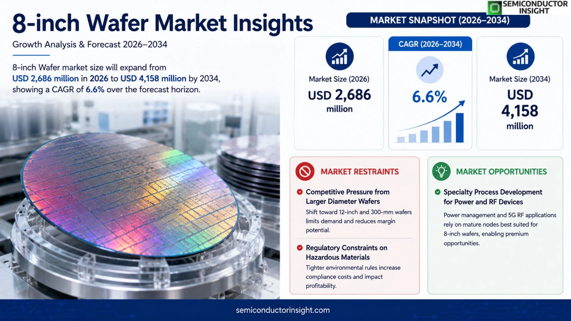
8-inch Wafer market size will expand from USD 2,686 million in 2026 to USD 4,158 million by 2034, showing a CAGR of 6.6% over the forecast horizon.
Semiconductor silicon wafers serve as the foundational substrate for integrated circuits that power computers, mobile devices and a broad range of electronic equipment. An 8‑inch wafer is a thin silicon disc that can be processed through polishing, epitaxial growth or oxidation to meet specific electrical and mechanical requirements; its high‑purity crystalline structure makes it ideal for logic, analog, power and sensor applications.
The sector’s expansion is linked to rising demand for power‑efficient devices such as electric‑vehicle drivetrains and industrial converters, which rely on high‑performance wafers for IGBTs and MOSFETs. Capacity additions reported by SEMI indicate a roughly 14% increase in global fab throughput between 2023 and 2026, while utilization rates are expected to climb toward 90% as manufacturers trim excess inventory. Recent supply‑chain moves,exemplified by Nexperia’s securing of local 8‑inch wafer sources for its 2026 production,highlight growing regionalization efforts aimed at mitigating geopolitical risk.
MARKET DRIVERS
Rising Demand for Advanced Semiconductor Nodes
The push toward finer process geometries has forced fabs to adopt 8‑inch wafers as a cost‑effective bridge before transitioning to larger diameters. Higher transistor density per wafer directly trims per‑chip expense, making this size attractive for mid‑range logic and power devices.
Expansion of Automotive and IoT Applications
Automotive electronics now require rugged, low‑power chips that are efficiently produced on 8‑inch platforms. Simultaneously, the explosion of IoT sensors,especially those embedded in edge devices,has created a steady stream of orders for mature‑node silicon, reinforcing the market’s momentum.
➤ “The convergence of automotive safety standards and edge‑computing workloads is reshaping capacity planning for 8‑inch lines,” notes a senior analyst at a leading semiconductor consultancy.
Combined, these trends elevate the strategic relevance of 8‑inch wafer Market, prompting manufacturers to modernize legacy lines with automation and yield‑enhancement tools.
MARKET CHALLENGES
Capital Intensity of Equipment Upgrades
Modernizing aging 8‑inch production equipment to meet today’s quality standards often demands multi‑million‑dollar outlays. Smaller players, in particular, struggle to justify such spending when larger‑diameter fabs promise economies of scale.
Other Challenges
Supply‑Chain Volatility
Fluctuations in the availability of high‑purity silicon and specialized photo‑resists create lead‑time extensions that can disrupt just‑in‑time manufacturing models.
MARKET RESTRAINTS
Competitive Pressure from Larger Diameter Wafers
Customers increasingly favor 12‑inch and 300‑mm platforms for high‑volume logic chips, leaving a narrowing niche for 8‑inch production. This shift erodes margin potential for firms that cannot diversify their product mix.
Regulatory Constraints on Hazardous Materials
Stringent environmental rules governing chemicals used in wafer processing raise compliance costs. Facilities that fail to adopt greener alternatives may face penalties that further compress profitability.
MARKET OPPORTUNITIES
Specialty Process Development for Power and RF Devices
Emerging power‑management modules and 5G RF front‑ends rely on mature process nodes that are optimally produced on 8‑inch wafers. Companies that tailor their lithography and doping recipes for these applications can capture premium pricing.
Strategic Partnerships with Foundry Service Providers
Forming joint ventures with global foundries enables smaller fabs to access advanced metrology and defect‑inspection tools without the full capital burden, unlocking new revenue streams within 8‑inch wafer Market.
Collectively, these pathways suggest that firms willing to invest in niche technology stacks and collaborative models are positioned to reap disproportionate benefits as the industry balances cutting‑edge scaling with cost‑sensitive production.
8-inch Wafer Market Trends
Supply Capacity and Utilization Pressures
The manufacturing footprint for 8-inch Wafer market is expanding modestly, with global 200 mm fab capacity projected to climb roughly 14 % between 2023 and 2026. Thirteen new volume fabs are slated to come online, pushing monthly throughput beyond 7.7 million units. Utilization metrics are tightening; average load is expected to move from the low‑70 % range in 2025 to the high‑80 % band by 2026. A pronounced uplift is visible in capacity earmarked for power‑device production, where growth outpaces the broader pool by about 35 %. This convergence of higher load factors and incremental capacity adds pressure on lead times, especially for customers locked into legacy 8‑inch toolsets.
Other Trends
Demand from Power and Automotive Segments
Electrification of transport and the rise of industrial drives are reshaping the demand profile of 8-inch Wafer market. Power‑semiconductor applications,such as IGBTs, MOSFETs and high‑voltage analog ICs,require wafers with stringent defect control, making epitaxial and thick‑SOI variants especially valuable. The shift toward higher‑efficiency power conversion has elevated the share of low‑doped, high‑resistivity substrates, prompting manufacturers to prioritize processes that improve gettering and surface passivation. As automotive OEMs accelerate EV roll‑outs, the need for reliable, high‑performance power wafers is translating into steadier order books for vendors that can supply differentiated wafer families.
Pricing Pressure and Mix Dynamics
Price behavior in 8-inch Wafer market remains tied to inventory cycles and product mix. Legacy wafer types are witnessing margin erosion as buyers pivot toward higher‑value epitaxial and annealed offerings, compressing the price floor for standard polished substrates. Concurrently, regional supply‑chain considerations are gaining prominence; recent moves by major Chinese manufacturers to secure local silicon wafer sources illustrate how geopolitical risk is prompting multi‑sourcing strategies. This shift not only buffers against cross‑border disruptions but also introduces variance in pricing across regions, compelling global customers to factor location‑based cost differentials into their procurement models.
COMPETITIVE LANDSCAPE
Key Industry Players
8‑inch Wafer Market – Competitive Overview
8‑inch wafer segment remains anchored by a handful of large‑scale silicon specialists whose production capacity and technology breadth shape pricing and supply‑chain dynamics. Shin‑Etsu Chemical, with its vertically integrated CZ and MCZ lines, commands the premium epitaxial and SOI niches, leveraging a mature customer base in power‑device and sensor applications. SUMCO follows closely, differentiating through a strong focus on high‑resistivity Float‑Zone material that serves high‑frequency analog and RF markets. Both firms benefit from long‑term fab contracts that lock in volume, allowing them to absorb short‑term demand swings while investing in incremental capacity upgrades at a measured pace. The market structure therefore resembles an oligopoly where the top two suppliers together capture roughly a third of global shipments, compelling smaller entrants to pursue specialized product mixes or regional sourcing strategies to stay viable.
Beyond the dominant duo, a diverse set of midsize and niche players sustains the breadth of the 8‑inch ecosystem. GlobalWafers and Siltronic have expanded their polished‑wafer portfolios to address analog and discrete‑device manufacturers, often coupling product launches with joint development programs. SK Siltron and FST Corporation specialize in engineered wafers such as thick‑SOI and annealed variants, targeting automotive power modules and MEMS sensors. Chinese‑origin firms,including Zhonghuan Advanced Semiconductor Materials, Hangzhou Lion Microelectronics, and Shanghai Advanced Silicon Technology,have accelerated capacity growth through state‑backed financing, narrowing the geographic gap with legacy vendors. Meanwhile boutique companies like GRINM Semiconductor Materials and ThinkonSemi carve out market share by supplying low‑dose doped wafers for emerging AI edge chips, where defect control and yield are paramount. This mix of scale, specialization, and regional ambition creates a competitive tapestry that pressures pricing while fostering innovation across the product spectrum.
List of Key 8‑inch Wafer Companies Profiled
- Shin‑Etsu Chemical
- SUMCO
- GlobalWafers
- Siltronic
- SK Siltron
- FST Corporation
- Zhonghuan Advanced Semiconductor Materials
- Hangzhou Lion Microelectronics
- Shanghai Advanced Silicon Technology (AST)
- GRINM Semiconductor Materials
- ThinkonSemi
- Episil‑Precision Inc.
Segment Analysis:
| Segment Category | Sub-Segments | Key Insights |
| By Type |
|
Polished Wafer remains the foundational substrate for a broad array of circuits.
|
| By Application |
|
MOSFET drives the most pronounced demand in the 8‑inch segment.
|
| By End User |
|
Power Electronics is the leading end‑user in the 8‑inch space.
|
| By Process Form |
|
Epitaxial Wafer is gaining prominence as process‑form choice.
|
| By Growth Method |
|
Magnetic Czochralski (MCZ) is the preferred method for high‑resistivity power wafers.
|
Regional Analysis: 8-inch Wafer Market
Operators in the region are augmenting wafer throughput through incremental line upgrades rather than whole‑plant builds, reflecting an emphasis on cost‑effective scaling. By repurposing existing cleanrooms for 8-inch production, firms can meet rising demand from automotive OEMs without incurring the expense of new silicon footprints, preserving financial flexibility in a volatile market.
Post‑pandemic lessons have spurred a diversification of raw‑material sources across Southeast Asia, diminishing reliance on single suppliers. This shift enhances 8-inch Wafer market’s ability to absorb shocks, while fostering regional logistics hubs that shorten delivery cycles for high‑volume customers.
Although 8-inch processes lag behind cutting‑edge nodes, the introduction of mature‑compatible immersion lithography tools has improved critical dimension control. This technology lift enables fab managers to push yields higher, reinforcing the value proposition of continuing 8-inch production alongside newer platforms.
Emerging environmental standards across China, Taiwan and South Korea require lower water‑usage cycles. Facilities are retrofitting recirculation systems, a move that simultaneously reduces operating costs and aligns with corporate sustainability mandates, influencing client selection criteria.
North America
North American fabs remain focused on high‑mix, low‑volume production, where 8-inch Wafer market serves niche applications such as aerospace and defense. The region’s competitive edge lies in its advanced engineering talent and proximity to major system integrators, enabling rapid design‑for‑manufacture cycles. However, higher labor and utility expenses compel manufacturers to prioritize value‑added services,like custom test and packaging,over simple volume scaling. Recent policy discussions around semiconductor resilience have encouraged modest investments in mature‑node capacity, yet the emphasis stays on maintaining a flexible, responsive supply chain for strategic customers rather than pursuing pure cost leadership.
Europe
Europe’s 8-inch Wafer Market reflects a continent‑wide strategy to preserve legacy production lines that support automotive safety and industrial automation sectors. Governments across Germany, France and the United Kingdom have introduced targeted subsidies to prevent the premature shutdown of mature‑node fabs, recognizing their role in employment and technological sovereignty. Manufacturers are leveraging these incentives to modernize equipment and integrate Industry 4.0 monitoring, thereby improving yield stability. The regional focus on high‑reliability products drives tighter quality controls, which, while increasing per‑wafer expense, satisfies stringent automotive standards and sustains demand for European‑produced silicon.
South America
In South America, 8-inch Wafer market is still embryonic, with most activity concentrated in Brazil’s emerging semiconductor clusters. Local demand is primarily driven by the renewable‑energy sector, where power‑management ICs require reliable, cost‑effective silicon. The region benefits from relatively low manufacturing wages, yet faces challenges in attracting advanced equipment due to limited financing options. Partnerships with Asian vendors have begun to bridge this gap, allowing South American fabs to assemble and test 8-inch wafers for regional customers, thereby reducing import dependence and fostering a nascent supply chain.
Middle East & Africa
The Middle East & Africa region views 8-inch Wafer market through the lens of diversification away from hydrocarbon‑centric economies. Emerging tech parks in the United Arab Emirates and Saudi Arabia are positioning themselves as hubs for mature‑node production, leveraging tax‑friendly regimes and strategic logistics corridors. While the talent pool is still developing, substantial investment in vocational training aims to create a skilled workforce capable of supporting wafer fabrication. Environmental considerations, particularly water scarcity, are prompting firms to adopt closed‑loop cooling systems, which align cost reduction with sustainability goals and may become a differentiator for regional players seeking global contracts.
Report Scope
This market research report provides a comprehensive analysis of the 8-inch Wafer Market , covering the forecast period 2026–2034. It offers detailed insights into market dynamics, technological advancements, competitive landscape, and key trends shaping the industry.
Key focus areas of the report include:
- Market Overview: The report begins with an overview outlining its current market scenario, key growth indicators, and industry transformation drivers. It discusses macroeconomic factors, demand–supply balance, regulatory landscape, and the strategic role of semiconductors in powering advancements across industries such as automotive, telecommunications, consumer electronics, and industrial automation.
- Market Size & Forecast: Historical data and future projections for revenue, unit shipments, and market value across major regions and segments.
- Segmentation Analysis: Detailed breakdown by product type, technology, application, and end-user industry to identify high-growth segments and investment opportunities.
- Regional Insights: Insights into market performance across North America, Europe, Asia-Pacific, Latin America, and the Middle East & Africa, including country-level analysis where relevant.
- Competitive Landscape: Profiles of leading market participants, including their product offerings, R&D focus, manufacturing capacity, pricing strategies, and recent developments such as mergers, acquisitions, and partnerships.
- Technology Trends & Innovation: Assessment of emerging technologies, integration of AI/IoT, semiconductor design trends, fabrication techniques, and evolving industry standards.
- Market Drivers & Restraints: Evaluation of factors driving market growth along with challenges, supply chain constraints, regulatory issues, and market-entry barriers.
- Stakeholder Insights: Insights for component suppliers, OEMs, system integrators, investors, and policymakers regarding the evolving ecosystem and strategic opportunities.
Primary and secondary research methods are employed, including interviews with industry experts, data from verified sources, and real-time market intelligence to ensure the accuracy and reliability of the insights presented.
FREQUENTLY ASKED QUESTIONS:
What is the current market size of 8-inch Wafer Market?
-> 8-inch Wafer market size will expand from USD 2,686 million in 2026 to USD 4,158 million by 2034, showing a CAGR of 6.6% over the forecast horizon.
Which key companies operate in 8-inch Wafer Market?
-> Key players include Shin‑Etsu Chemical, SUMCO, GlobalWafers, Siltronic, SK Siltron, FST Corporation, Wafer Works Corporation, National Silicon Industry Group (NSIG), Zhonghuan Advanced Semiconductor Materials, Hangzhou Lion Microelectronics, Hangzhou Semiconductor Wafer, GRINM Semiconductor Materials, Shanghai Advanced Silicon Technology (AST), Soitec, Hebei Puxing Electronic Technology, Nanjing Guosheng Electronics, MCL Electronic Materials, ThinkonSemi, Episil‑Precision Inc..
What are the key growth drivers?
-> Key growth drivers include electrification of transportation (EV/HEV), industrial drives, energy‑infrastructure upgrades, and the expanding demand for power‑management semiconductors that boost 200 mm wafer consumption, especially for IGBTs, MOSFETs and power‑device applications.
Which region dominates the market?
-> Asia-Pacific remains the dominant region, driven by strong manufacturing bases in China, Japan, and South Korea, while also showing the highest growth rates.
What are the emerging trends?
-> Emerging trends include increased adoption of engineered wafers such as thick‑SOI and annealed wafers, higher utilization of magnetic Czochralski (MCZ) growth for improved resistivity, and regional supply‑chain localization efforts to mitigate geopolitical risks.

Get Sample Report PDF for Exclusive Insights
Report Sample Includes
- Table of Contents
- List of Tables & Figures
- Charts, Research Methodology, and more...
 Download Sample Report PDF






