
Key Statistics
Key Takeaways
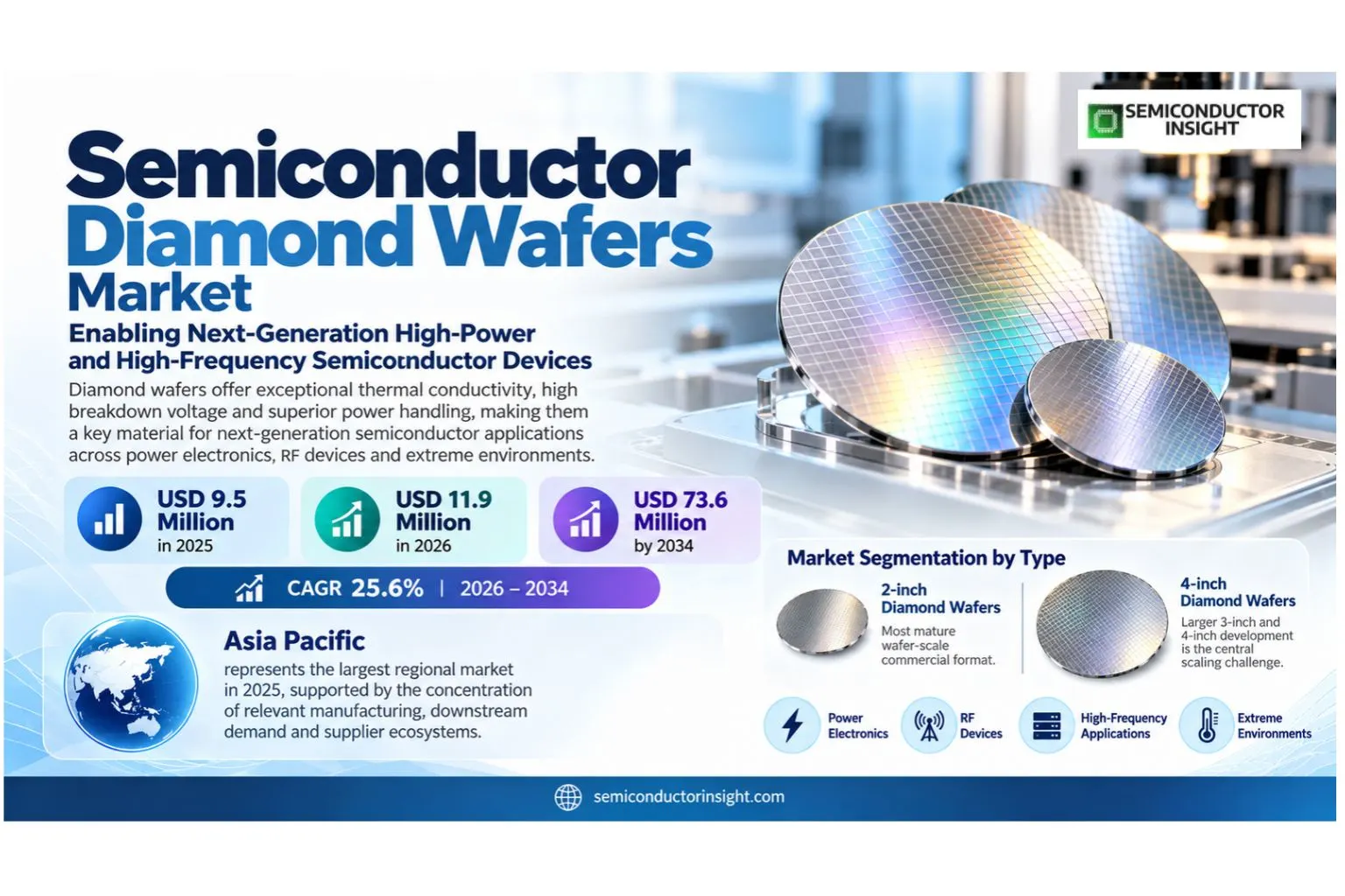
- Semiconductor diamond wafers market was valued at USD 9.5 million in 2025 and is projected to reach USD 73.6 million by 2034, representing a 25.6% CAGR over 2026–2034.
- The market is valued at USD 9.47 million in 2025 and is projected to reach USD 73.64 million by 2034, representing a 25.6% CAGR over 2026–2034.
- 2-inch single-crystal wafers remain the nearest-term commercial format, while 3-inch and 4-inch development is critical to improve device area, process compatibility and manufacturing economics.
- RF power and power electronics are the most established semiconductor applications because diamond’s exceptional thermal conductivity can remove heat directly from high-power GaN and SiC devices.
- Asia Pacific leads through Japanese wafer-scale diamond development and a growing Chinese materials base, while North America is a major commercialization market for AI, RF and defense thermal management.
Semiconductor Diamond Wafers Market Overview
Semiconductor diamond wafers market was valued at USD 9.5 million in 2025, is estimated at USD 11.9 million in 2026, and is projected to reach USD 73.6 million by 2034, advancing at a 25.6% CAGR during 2026–2034. Asia Pacific represents the largest regional market in 2025, supported by the concentration of relevant manufacturing, downstream demand and supplier ecosystems.
Semiconductor diamond wafers are synthetic diamond substrates or bonded diamond layers engineered for electronic devices and semiconductor thermal management. Diamond combines exceptionally high thermal conductivity with wide bandgap, high breakdown field and high carrier velocity, making it attractive where heat limits the performance of GaN, SiC, RF and high-power compute systems.
The near-term market is centered on thermal substrates and wafer bonding rather than fully monolithic diamond electronics. Commercial progress depends on scaling single-crystal area, lowering cost, controlling defects and creating bond interfaces with low thermal resistance. Wafer-size milestones therefore matter directly to adoption.
The commercial structure of the semiconductor diamond wafers market is shaped by design qualification, production economics and the interaction between component performance and downstream system requirements. Suppliers that can combine consistent manufacturing, application engineering and supply assurance are better positioned to convert technical eligibility into repeat business. Customer decisions increasingly account for lifecycle continuity, geographic resilience and integration cost, which makes proven process control and ecosystem compatibility as important as nominal product capability.
Segment Analysis: By Type
By type, the Semiconductor Diamond Wafers market is segmented into 2-inch Diamond Wafers, 4-inch Diamond Wafers. 2-inch wafers represent the most mature wafer-scale commercial format, while larger 3-inch and 4-inch development is the central scaling challenge. As diameter increases, maintaining crystal uniformity and low defect density becomes substantially harder. Purchasing decisions vary by performance requirement, qualification burden, integration complexity and lifecycle economics, so suppliers compete on application fit rather than on a single technical specification.
| Type | Role in the market | Demand characteristics |
|---|---|---|
| 2-inch Diamond Wafers | 2-inch Diamond Wafers addresses a distinct part of the product and process mix. Its commercial position depends on technical fit, manufacturing maturity, integration requirements and customer qualification rather than on headline specifications alone. | Demand is strongest where the segment aligns with established customer designs, predictable supply, and measurable system-level performance. Suppliers that can document repeatability, compatibility and lifecycle support are better placed to defend design wins. |
| 4-inch Diamond Wafers | 4-inch Diamond Wafers addresses a distinct part of the product and process mix. Its commercial position depends on technical fit, manufacturing maturity, integration requirements and customer qualification rather than on headline specifications alone. | Demand is strongest where the segment aligns with established customer designs, predictable supply, and measurable system-level performance. Suppliers that can document repeatability, compatibility and lifecycle support are better placed to defend design wins. |
Segment Analysis: By Material Form
By material form, the Semiconductor Diamond Wafers market is segmented into Single-Crystal Diamond, Polycrystalline / Composite Diamond. Single-crystal diamond provides the highest thermal performance and best wafer-bonding potential, while polycrystalline and composite materials can offer lower-cost thermal management for broader packages. Purchasing decisions vary by performance requirement, qualification burden, integration complexity and lifecycle economics, so suppliers compete on application fit rather than on a single technical specification.
| Material Form | Role in the market | Demand characteristics |
|---|---|---|
| Single-Crystal Diamond | Single-Crystal Diamond represents a relevant purchasing and deployment pathway within this market. Commercial attractiveness depends on how well it aligns with customer architecture, supply-chain constraints and required performance. | Growth is linked to design-in activity, installed-base transitions and the ability of suppliers to meet qualification, cost and availability requirements over the full product lifecycle. |
| Polycrystalline / Composite Diamond | Polycrystalline / Composite Diamond represents a relevant purchasing and deployment pathway within this market. Commercial attractiveness depends on how well it aligns with customer architecture, supply-chain constraints and required performance. | Growth is linked to design-in activity, installed-base transitions and the ability of suppliers to meet qualification, cost and availability requirements over the full product lifecycle. |
Segment Analysis: By Application
By application, the Semiconductor Diamond Wafers market is segmented into RF Power, 5G & Satellites, Power Electronics, Cloud & AI Compute. RF power and power electronics provide the clearest value because hotspot temperature directly limits device output and reliability. AI and HPC are emerging as important applications as GPU and accelerator packages exceed the thermal capability of conventional spreaders. Purchasing decisions vary by performance requirement, qualification burden, integration complexity and lifecycle economics, so suppliers compete on application fit rather than on a single technical specification.
| Application | Role in the market | Demand characteristics |
|---|---|---|
| RF Power, 5G & Satellites | RF Power, 5G & Satellites creates demand when the underlying system requires the market’s core function at production scale. Procurement is normally tied to platform launches, equipment upgrades, capacity expansion or replacement cycles. | Buyers evaluate reliability, qualification time, integration cost and vendor support alongside unit economics. Adoption accelerates when the solution removes a system bottleneck or supports a new performance tier without creating disproportionate redesign risk. |
| Power Electronics | Power Electronics creates demand when the underlying system requires the market’s core function at production scale. Procurement is normally tied to platform launches, equipment upgrades, capacity expansion or replacement cycles. | Buyers evaluate reliability, qualification time, integration cost and vendor support alongside unit economics. Adoption accelerates when the solution removes a system bottleneck or supports a new performance tier without creating disproportionate redesign risk. |
| Cloud & AI Compute | Cloud & AI Compute creates demand when the underlying system requires the market’s core function at production scale. Procurement is normally tied to platform launches, equipment upgrades, capacity expansion or replacement cycles. | Buyers evaluate reliability, qualification time, integration cost and vendor support alongside unit economics. Adoption accelerates when the solution removes a system bottleneck or supports a new performance tier without creating disproportionate redesign risk. |
Segment Analysis: By Integration Route
By integration route, the Semiconductor Diamond Wafers market is segmented into Direct Bonding, Diamond-on-Semiconductor, Standalone Diamond Substrate. Direct wafer bonding reduces thermal interface resistance, diamond-on-semiconductor combines proven active materials with diamond cooling, and standalone substrates support device research and specialty structures. Purchasing decisions vary by performance requirement, qualification burden, integration complexity and lifecycle economics, so suppliers compete on application fit rather than on a single technical specification.
| Integration Route | Role in the market | Demand characteristics |
|---|---|---|
| Direct Bonding | Direct Bonding represents a relevant purchasing and deployment pathway within this market. Commercial attractiveness depends on how well it aligns with customer architecture, supply-chain constraints and required performance. | Growth is linked to design-in activity, installed-base transitions and the ability of suppliers to meet qualification, cost and availability requirements over the full product lifecycle. |
| Diamond-on-Semiconductor | Diamond-on-Semiconductor represents a relevant purchasing and deployment pathway within this market. Commercial attractiveness depends on how well it aligns with customer architecture, supply-chain constraints and required performance. | Growth is linked to design-in activity, installed-base transitions and the ability of suppliers to meet qualification, cost and availability requirements over the full product lifecycle. |
| Standalone Diamond Substrate | Standalone Diamond Substrate represents a relevant purchasing and deployment pathway within this market. Commercial attractiveness depends on how well it aligns with customer architecture, supply-chain constraints and required performance. | Growth is linked to design-in activity, installed-base transitions and the ability of suppliers to meet qualification, cost and availability requirements over the full product lifecycle. |
Regional Analysis
Asia Pacific leads the semiconductor diamond wafers market in 2025, while regional growth patterns differ according to manufacturing concentration, customer investment cycles, regulation, product mix and supply-chain access. The most important regional distinction is not simply market size; it is the mechanism that converts local investment and end-market demand into qualified purchases.
How does regional demand differ across the semiconductor diamond wafers market?
Regional demand for semiconductor diamond wafers is structurally uneven because manufacturing assets, design centers, downstream customers and qualification ecosystems are not distributed evenly. Asia Pacific typically has the deepest electronics manufacturing base, North America combines technology development with capital investment, Europe emphasizes reliability and industrial requirements, and emerging regions are more dependent on imported systems. These differences influence vendor selection, inventory policy, service expectations and the pace at which new technologies are adopted.
| Region | Market position | Growth outlook | Demand profile | Supplier-selection gate |
|---|---|---|---|---|
| Asia Pacific | Largest | Very strong | Wafer-scale materials development led | Crystal size, yield and manufacturing cost |
| North America | Major commercialization market | Very strong | AI, RF and defense thermal demand led | Cost and integration qualification |
| Europe | Advanced materials market | Strong | Research, RF and power electronics led | Wafer scaling and integration |
| South America | Nascent | Selective | Research led | Cost and local semiconductor ecosystem |
| Middle East & Africa | Early-stage | Selective | Research, RF and technology investment led | Cost and advanced manufacturing access |
Detailed Regional Blocks
Competitive Landscape
Competition in the semiconductor diamond wafers market is determined by technical qualification, manufacturing consistency, customer relationships and the ability to support product lifecycles. Price matters, but it rarely overrides reliability, integration effort or switching cost once a supplier has been designed into a production platform.
The competitive field includes Diamond Foundry, Orbray, Diamond Materials, AKHAN Semiconductor, Diamfab, Origin Stone Element, alongside other specialized suppliers. Market share can shift when a vendor gains access to a new platform, expands qualified capacity or introduces a technology that materially improves system performance. Because customer validation can be lengthy, incumbent suppliers often benefit from continuity, while challengers need a clear technical or supply-chain advantage to displace an approved source.
Competitive strategy is increasingly multi-dimensional. Leading suppliers invest in process or product development, application engineering and regional support at the same time, while customers seek second-source options where technically feasible. This creates a market in which differentiation is sustained through documented performance, manufacturing yield, quality systems, responsiveness and the ability to support future roadmap transitions without forcing unnecessary redesigns.
| Company | Competitive position | Primary basis of competition |
|---|---|---|
| Diamond Foundry | Established global / strategic supplier | Competes through product capability, qualification, account access and supply execution. |
| Orbray | Established global / strategic supplier | Competes through product capability, qualification, account access and supply execution. |
| Diamond Materials | Established global / strategic supplier | Competes through product capability, qualification, account access and supply execution. |
| AKHAN Semiconductor | Specialist / regional competitor | Competes through product capability, qualification, account access and supply execution. |
| Diamfab | Specialist / regional competitor | Competes through product capability, qualification, account access and supply execution. |
| Origin Stone Element | Specialist / regional competitor | Competes through product capability, qualification, account access and supply execution. |
| Applied Diamond | Focused challenger / niche participant | Competes through product capability, qualification, account access and supply execution. |
| Element Six | Focused challenger / niche participant | Competes through product capability, qualification, account access and supply execution. |
| Compound Semiconductor (Xiamen) Technology | Focused challenger / niche participant | Competes through product capability, qualification, account access and supply execution. |
Production Capacity Analysis
Capacity is constrained by CVD crystal-growth time, seed quality, polishing, wafer flatness and defect control. The industry is still transitioning from small plates toward repeatable multi-inch single-crystal wafers, so qualified area is scarce.
Element Six and Orbray are advancing 2-inch, 3-inch and future 4-inch wafer formats, while other suppliers focus on diamond substrates, heat spreaders and early semiconductor structures. Volume production remains far smaller than silicon or SiC.
Capacity should therefore be evaluated on a qualified-output basis rather than as nominal installed capability. A supplier may possess equipment or production lines that appear suitable but still require customer-specific validation, process tuning, test correlation or upstream material qualification. This distinction becomes especially important during demand spikes, when headline capacity can overstate the volume that is immediately available for a particular application, technology generation or reliability class.
Market Dynamics
The semiconductor diamond wafers market is being shaped by rising performance requirements and technology transitions on the demand side, while qualification complexity, supply concentration and cost discipline constrain the pace of adoption. The balance of these forces favors suppliers that can solve a measurable system problem without increasing integration risk.
Demand expansion is not uniform across all product variants or customer groups. New technology creates attractive design opportunities, but buyers typically require a clear economic or performance case before changing a qualified architecture. At the same time, supply-chain localization, capacity investment and tighter quality requirements are changing procurement behavior. As a result, growth is likely to concentrate around applications where performance upgrades, manufacturing scale and lifecycle value reinforce one another.
Market Drivers
Four forces provide the strongest support for demand in the semiconductor diamond wafers market: performance-driven technology upgrades, expansion of relevant downstream applications, investment in manufacturing or infrastructure, and the need for more resilient supply. Their importance varies by segment, but each creates a direct reason for customers to qualify or purchase additional solutions.
| Driver | Impact | Commercial mechanism |
|---|---|---|
| AI and RF heat flux exceeds conventional materials | High | Diamond can spread heat from localized hotspots more effectively than copper or ceramics. |
| Wafer bonding enables hybrid semiconductor stacks | High | Diamond can be bonded to GaN, SiC or silicon without replacing established active-device materials. |
| Larger single-crystal wafers improve manufacturing economics | Medium-High | Scaling beyond small plates makes lithographic semiconductor processing more practical. |
| Power electronics need higher junction-temperature margin | Medium-High | Better heat removal can raise device output or extend lifetime. |
AI and RF heat flux exceeds conventional materials
Diamond can spread heat from localized hotspots more effectively than copper or ceramics. The commercial effect is strongest where customers can link the technology change to higher throughput, lower power, improved reliability, reduced lifecycle cost or access to a new end-market requirement.
Wafer bonding enables hybrid semiconductor stacks
Diamond can be bonded to GaN, SiC or silicon without replacing established active-device materials. The commercial effect is strongest where customers can link the technology change to higher throughput, lower power, improved reliability, reduced lifecycle cost or access to a new end-market requirement.
Larger single-crystal wafers improve manufacturing economics
Scaling beyond small plates makes lithographic semiconductor processing more practical. The commercial effect is strongest where customers can link the technology change to higher throughput, lower power, improved reliability, reduced lifecycle cost or access to a new end-market requirement.
Power electronics need higher junction-temperature margin
Better heat removal can raise device output or extend lifetime. The commercial effect is strongest where customers can link the technology change to higher throughput, lower power, improved reliability, reduced lifecycle cost or access to a new end-market requirement.
Market Restraints
Growth is moderated by qualification burden, cyclical purchasing, technology substitution and supply-chain risk. These restraints do not eliminate demand, but they can extend sales cycles, limit supplier switching and reduce the speed at which technically superior solutions convert into production revenue.
| Restraint | Impact | Commercial consequence |
|---|---|---|
| Single-crystal diamond is expensive | High | CVD growth and finishing are slow and capital intensive. |
| Large-area defect-free growth is difficult | High | Crystal boundaries, stress and surface quality become harder to control at larger diameter. |
| Bonding interfaces can limit thermal benefit | Medium | Poor interface quality adds thermal resistance that reduces the advantage of diamond. |
| SiC, GaN and advanced packaging continue improving | Medium | Alternative materials can meet many applications at lower cost. |
Single-crystal diamond is expensive
CVD growth and finishing are slow and capital intensive. Suppliers can mitigate part of this pressure through stronger qualification support, transparent lifecycle planning, dual-source strategies and better alignment between product roadmaps and customer production schedules.
Large-area defect-free growth is difficult
Crystal boundaries, stress and surface quality become harder to control at larger diameter. Suppliers can mitigate part of this pressure through stronger qualification support, transparent lifecycle planning, dual-source strategies and better alignment between product roadmaps and customer production schedules.
Bonding interfaces can limit thermal benefit
Poor interface quality adds thermal resistance that reduces the advantage of diamond. Suppliers can mitigate part of this pressure through stronger qualification support, transparent lifecycle planning, dual-source strategies and better alignment between product roadmaps and customer production schedules.
SiC, GaN and advanced packaging continue improving
Alternative materials can meet many applications at lower cost. Suppliers can mitigate part of this pressure through stronger qualification support, transparent lifecycle planning, dual-source strategies and better alignment between product roadmaps and customer production schedules.
Market Opportunities
The most attractive opportunities in the semiconductor diamond wafers market occur where a technology transition creates measurable value and where suppliers can enter before the customer architecture is locked. Early engagement, application-specific engineering and credible supply planning can convert these windows into durable design positions.
3-inch and 4-inch wafer scale
Larger wafers can unlock semiconductor-compatible batch processing and better cost per area. The opportunity is strongest for suppliers that can demonstrate performance with production-relevant data, provide engineering support during qualification and maintain a roadmap that gives customers confidence in long-term availability.
Direct-bonded GaN-on-diamond
RF amplifiers can benefit from heat removal close to the active region. The opportunity is strongest for suppliers that can demonstrate performance with production-relevant data, provide engineering support during qualification and maintain a roadmap that gives customers confidence in long-term availability.
AI accelerator thermal spreaders
GPU and HBM packages need new materials as package power rises. The opportunity is strongest for suppliers that can demonstrate performance with production-relevant data, provide engineering support during qualification and maintain a roadmap that gives customers confidence in long-term availability.
High-voltage diamond electronics
Longer-term devices could exploit diamond’s own wide-bandgap properties rather than only its thermal conductivity. The opportunity is strongest for suppliers that can demonstrate performance with production-relevant data, provide engineering support during qualification and maintain a roadmap that gives customers confidence in long-term availability.
Supply Chain Analysis
Synthetic diamond growth
Microwave plasma CVD and related methods grow high-purity single-crystal or polycrystalline diamond. Value capture at this stage depends on quality consistency, technical differentiation and the difficulty of substitution. Bottlenecks can propagate downstream when qualification or material compatibility prevents customers from shifting quickly to an alternative supplier.
Wafer finishing
Diamond is sliced, polished and characterized for thickness, flatness and surface quality. Value capture at this stage depends on quality consistency, technical differentiation and the difficulty of substitution. Bottlenecks can propagate downstream when qualification or material compatibility prevents customers from shifting quickly to an alternative supplier.
Bonding and integration
Diamond is bonded to GaN, SiC, silicon or package structures for thermal management. Value capture at this stage depends on quality consistency, technical differentiation and the difficulty of substitution. Bottlenecks can propagate downstream when qualification or material compatibility prevents customers from shifting quickly to an alternative supplier.
Device and package deployment
RF, power, AI and research systems integrate diamond where thermal performance justifies cost. Value capture at this stage depends on quality consistency, technical differentiation and the difficulty of substitution. Bottlenecks can propagate downstream when qualification or material compatibility prevents customers from shifting quickly to an alternative supplier.
Recent Developments
Recent developments show how technology roadmaps, manufacturing investment and standards are changing the competitive requirements of the semiconductor diamond wafers market. The entries below are selected for their direct relevance to product capability, capacity, qualification or downstream adoption rather than for general corporate activity.
Element Six and Orbray announced a reproducible 3-inch single-crystal diamond wafer process, 4-inch development and preparation of 2-inch thermal-bonding wafers for volume production. Source
Element Six introduced a copper-diamond composite designed for AI, HPC and GaN RF devices, highlighting growing semiconductor demand for diamond-class thermal performance. Source
Element Six continues to position WSC wafer single-crystal synthetic diamond for direct wafer-level bonding in advanced power and RF electronics and high-power compute thermal management. Source
Report Scope & Segmentation
| Report attribute | Coverage |
|---|---|
| Market | Semiconductor Diamond Wafers |
| Base Year | 2025 |
| Estimated Year | 2026 |
| Forecast Period | 2026–2034 |
| 2025 Market Size | USD 9.5 million |
| 2026 Estimated Size | USD 11.9 million |
| 2034 Forecast Size | USD 73.6 million |
| CAGR (2026–2034) | 25.6% |
| Largest Market in 2025 | Asia Pacific |
| By Type | 2-inch Diamond Wafers, 4-inch Diamond Wafers |
| By Application | RF Power, 5G & Satellites, Power Electronics, Cloud & AI Compute |
| By Material Form | Single-Crystal Diamond, Polycrystalline / Composite Diamond |
| By Integration Route | Direct Bonding, Diamond-on-Semiconductor, Standalone Diamond Substrate |
| Companies Profiled | Diamond Foundry, Orbray, Diamond Materials, AKHAN Semiconductor, Diamfab, Origin Stone Element, Applied Diamond, Element Six, Compound Semiconductor (Xiamen) Technology |
Frequently Asked Questions
What was the semiconductor diamond wafers market size in 2025?
The global semiconductor diamond wafers market was valued at USD 9.5 million in 2025. The 2025 value is the base-year reference used throughout this overview and provides the starting point for comparing the 2026 estimate and the 2034 forecast.
What is the projected semiconductor diamond wafers market size in 2034?
The global market is projected to reach USD 73.6 million by 2034. The forecast reflects the interaction of downstream adoption, technology transitions, production investment and the qualification requirements that shape commercial conversion across the market.
What is the CAGR of the semiconductor diamond wafers market from 2026 to 2034?
The semiconductor diamond wafers market is expected to expand at a 25.6% CAGR during 2026–2034. Growth will not be uniform across every product or region because customer qualification, capital cycles, supply constraints and application-specific performance requirements differ materially.
Which region is the largest semiconductor diamond wafers market?
Asia Pacific is the largest regional market in 2025. Its position is supported by the concentration of relevant manufacturing, customers, technology ecosystems and downstream demand, although the precise commercial mechanism differs by country and application.
How is the semiconductor diamond wafers market segmented by type?
By type, the market is segmented into 2-inch Diamond Wafers, 4-inch Diamond Wafers. These categories address different performance, cost and integration requirements, so supplier selection depends on application fit, qualification history and lifecycle economics rather than a single specification.
What are the main applications for semiconductor diamond wafers?
By application, the market covers RF Power, 5G & Satellites, Power Electronics, Cloud & AI Compute. Demand in each application is linked to platform launches, capacity expansion, equipment replacement and the degree to which the technology improves system performance or manufacturing economics.
What are the principal growth drivers for the semiconductor diamond wafers market?
Key drivers include ai and rf heat flux exceeds conventional materials and wafer bonding enables hybrid semiconductor stacks. These forces increase demand when customers can translate technical improvements into higher performance, lower cost, greater reliability or access to new applications.
What are the main restraints in the semiconductor diamond wafers market?
Important restraints include single-crystal diamond is expensive and large-area defect-free growth is difficult. The resulting qualification burden, purchasing cyclicality and technology risk can extend sales cycles and limit rapid supplier substitution even when new solutions offer clear technical advantages.
Which companies participate in the semiconductor diamond wafers market?
Companies profiled in this market include Diamond Foundry, Orbray, Diamond Materials, AKHAN Semiconductor, Diamfab, Origin Stone Element, Applied Diamond, Element Six. Competition centers on qualification, product or process performance, manufacturing consistency, customer support and the ability to maintain supply across the required product lifecycle.
What should buyers evaluate when selecting a semiconductor diamond wafers supplier?
Buyers should evaluate demonstrated performance, qualification history, manufacturing consistency, lifecycle support, supply resilience and integration cost. A technically strong product can still face adoption barriers if it increases redesign risk, lacks regional support or cannot meet the customer’s production and quality requirements.
Research Sources & Evidence Base
View research sources used for this overview.
- Element Six. Element Six and Orbray partnership — 2026 3-inch single-crystal wafer milestone, 4-inch development and 2-inch volume plans.
- Element Six. Thermal Management — WSC wafer single-crystal diamond and semiconductor thermal-management applications.
- Element Six. Semiconductor Solutions — Diamond heat-spreader applications in GaN RF, GPUs, AI accelerators and HBM packages.
- Element Six. Cu-Diamond launch — 2025 commercialization of diamond composite thermal-management material for AI, HPC and RF.
Get Sample Report PDF for Exclusive Insights
Report Sample Includes
- Table of Contents
- List of Tables & Figures
- Charts, Research Methodology, and more...
 Download Sample Report PDF





