Automotive electrification, industrial drives and high-efficiency power conversion translate into demanding device and material qualification programs, including 200 mm roadmaps.
Key Statistics
2025 Market Size
USD 755.5 million
2034 Projected Size
USD 2.76 billion
Largest Market in 2025
Asia Pacific
Key Takeaways
- 6-inch SiC substrates are the installed production core, while 8-inch material is the strategic transition segment as suppliers and device makers move toward 200 mm manufacturing.
- Power devices are the core application, supported by electric-vehicle inverters, charging, renewable-energy conversion and industrial drives that value high-voltage efficiency.
- Asia Pacific is the largest regional market because it combines substrate suppliers, power-device fabrication, vehicle production and electronics manufacturing at scale.
- 200 mm commercialization is the key structural shift: Wolfspeed launched a commercial 200 mm materials portfolio in September 2025 and Coherent had begun 200 mm epi-wafer shipments in 2024.
- Crystal defects, wafering difficulty and cost remain major restraints because saleable output depends on low-defect crystal growth and repeatable downstream processing rather than furnace count alone.
Silicon Carbide (SiC) Substrate Market Overview
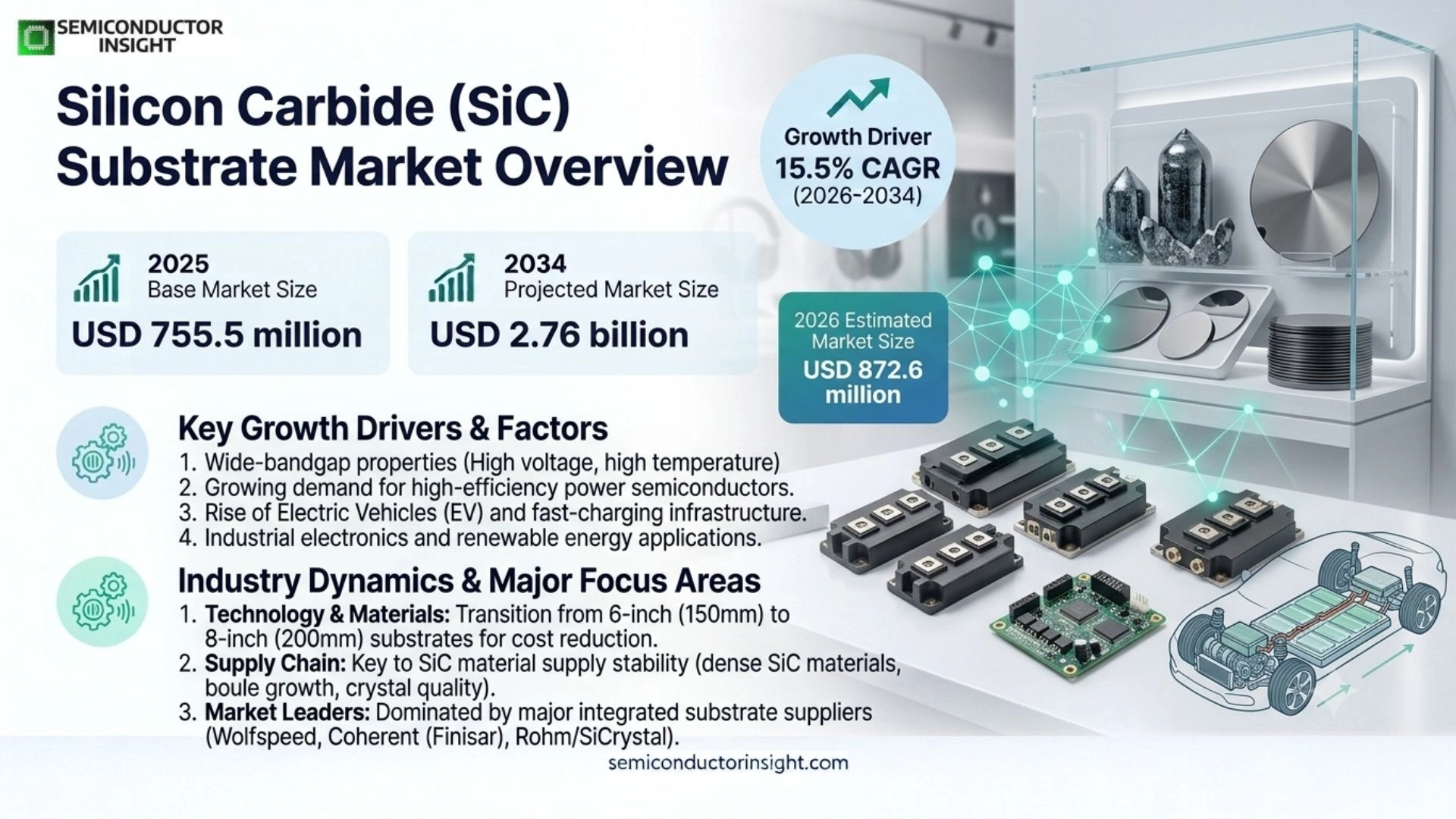
The global Silicon Carbide (SiC) substrate market is valued at USD 755.5 million in 2025 and is projected to reach USD 2.76 billion by 2034, representing a 15.5% CAGR during 2026–2034. The 2026 estimated market size is USD 872.6 million. Asia Pacific is the largest market, supported by dense SiC materials, power-semiconductor, electric-vehicle and industrial-electronics supply chains.
Base year: 2025 · Estimated year: 2026 · Forecast period: 2026–2034 · Historical data: 2021–2025 · Values in USD
Silicon carbide substrates are single-crystal wafers that form the foundation for SiC epitaxy and power or radio-frequency semiconductor devices. Their commercial value comes from enabling devices that operate at higher voltage, temperature and switching frequency than conventional silicon alternatives. Substrate quality therefore affects epitaxial performance, device yield and final system economics, making material consistency and qualification central purchasing criteria.
The report scope covers 4-inch, 6-inch and 8-inch substrates used in power devices, RF devices and other specialty applications. Demand depends on diameter, defect density, wafer bow, surface finish and compatibility with the customer’s epitaxy and device flow. Because material changes can affect downstream yield and reliability, supplier relationships become technically sticky after qualification.
The most important manufacturing transition is the move from 150 mm to 200 mm. Coherent states that 200 mm provides 1.8 times more usable area per wafer, while Wolfspeed commercially launched 200 mm SiC materials in September 2025. Larger wafers can improve die output per process cycle, but only when crystal and wafer quality remain stable through scale-up.
Segment Analysis: By Type
By substrate diameter, the report segments the market into 4 Inch, 6 Inch and 8 Inch. Six-inch wafers form the established commercial production core, while 8-inch material is the fastest strategic transition because larger wafers can improve wafer-level productivity and align SiC manufacturing with 200 mm semiconductor infrastructure.
| Type |
Manufacturing role |
Market position |
| 4 Inch |
Legacy and specialty diameter used in mature SiC lines, development environments and selected RF applications where existing tooling and qualification history remain more important than scale economics. |
A mature segment with declining strategic importance in mainstream automotive power devices, but still relevant for specialty processes and low-volume applications where tool conversion is uneconomic. |
| 6 Inch |
The established 150 mm platform for commercial SiC substrate, epitaxy and power-device production, supported by broad equipment compatibility and years of qualification experience. |
Largest installed base. It remains the practical volume anchor because material quality and device yield are proven at scale, although new capital programs increasingly include a 200 mm transition path. |
| 8 Inch |
The 200 mm platform intended to raise die output per process cycle and improve manufacturing productivity. It requires tighter control of crystal quality, geometry and epitaxy uniformity. |
Fastest strategic transition. Coherent began 200 mm epi-wafer shipments in 2024 and cited 1.8 times more usable area, while Wolfspeed launched a commercial 200 mm materials portfolio in 2025. |
Secondary segmentation
The second segmentation axis is application. Power devices use SiC for efficient high-voltage switching, RF devices use the material system for demanding microwave and telecom environments, and other uses include specialized high-temperature electronics. Power devices set the volume trajectory because electric mobility and energy conversion create recurring wafer demand across several device families.
| Axis |
Segments |
Commercial implication |
| Application |
Power Device · RF Devices · Others |
Power devices provide the broadest demand base; RF and specialty uses support differentiated specifications and high-value qualification niches. |
Segment Analysis: By Application
By application, Power Device demand is the central volume driver, while RF devices and other specialty uses support smaller but technically demanding niches. Electric vehicles, charging, renewable-energy inverters, industrial drives and grid conversion systems all convert efficiency requirements into demand for qualified SiC material.
| Application |
Demand characteristics |
| Power Device |
The largest application group covers MOSFETs, diodes and related high-voltage switching devices used in traction inverters, on-board chargers, industrial drives and renewable-energy conversion. The IEA reports more than 20 million electric cars sold globally in 2025, reinforcing a large end-market base for efficient power electronics. |
| RF Devices |
SiC substrates support high-frequency device structures, including GaN-on-SiC approaches, where thermal robustness and microwave performance matter. Volumes are lower than power electronics, but buyers can pay for material consistency because substrate quality influences RF device performance and reliability. |
| Others |
Specialty aerospace, research, harsh-environment and high-temperature electronics create smaller but durable demand. These markets often prioritize traceability, non-standard specifications and long availability over lowest unit cost, allowing technically capable suppliers to defend premium niches. |
Regional Analysis
Asia Pacific leads the SiC substrate market because it combines substrate producers, automotive and electronics manufacturing, power-semiconductor capacity and rapidly scaling electric-vehicle supply chains. North America remains strategically important through Wolfspeed and Coherent, while Europe is a major demand center for automotive and industrial power semiconductors.
How does regional demand differ across the Silicon Carbide substrate market?
Regional competition is defined by where crystal growth, wafer conversion, epitaxy, device fabrication and customer qualification occur. Asia Pacific benefits from manufacturing density and multiple domestic suppliers. North America has leading materials know-how and large capacity programs. Europe converts automotive and industrial demand into long-term material qualifications. South America and the Middle East & Africa are primarily downstream power-electronics markets.
| Region |
Position |
Growth outlook |
Demand profile |
Supplier selection |
| Asia Pacific |
Largest market |
High |
Manufacturing & EV led |
Material quality, local supply, diameter transition and device qualification |
| North America |
Strategic materials hub |
High |
Capacity & technology led |
200 mm readiness, long-term supply and defect performance |
| Europe |
Major device demand center |
High |
Automotive & industrial |
Reliability qualification and integrated device roadmaps |
| South America |
Emerging downstream |
Moderate |
Import led |
Availability, landed cost and technical support |
| Middle East & Africa |
Emerging downstream |
Moderate |
Energy & infrastructure |
Supply reliability and project qualification |
Asia Pacific LARGEST MARKET
Why does Asia Pacific lead SiC substrate demand?
China, Japan and South Korea combine material production, device manufacturing and large EV/electronics ecosystems, creating the deepest recurring wafer demand.
Market positionLargest
Growth outlookHigh
Demand profileManufacturing & EV
Commercial gateDevice qualification
| Country / market |
Role |
Demand mechanism |
| China |
Scale growth |
Local substrate suppliers and the world’s largest EV manufacturing base support strong demand for qualified domestic material. |
| Japan & South Korea |
Technology base |
Materials science, automotive electronics and semiconductor manufacturing support high-specification demand and export-oriented supply. |
Market instances
- China’s EV manufacturing scale amplifies upstream demand. The IEA reports that China produced 12.4 million electric cars in 2024, creating a large installed base for power-device production and qualification.
- 200 mm qualification is becoming a competitive window. Suppliers that demonstrate stable geometry and defect performance early can win positions before large-diameter processes become fully mature.
In the full report: country-level market size, segment metrics and forecast analysis across the report window.
North America STRATEGIC MATERIALS HUB
What makes North America strategically important?
Wolfspeed and Coherent have major SiC materials capabilities and have invested in 200 mm scaling, influencing global technology and supply agreements even when downstream assembly occurs elsewhere.
Market positionStrategic supply hub
Growth outlookHigh
Demand profileCapacity & technology
Commercial gate200 mm qualification
| Country / market |
Role |
Demand mechanism |
| United States |
Core supply hub |
Wolfspeed and Coherent programs connect crystal growth, substrate and epitaxial-wafer supply with automotive, industrial and energy customers. |
| Mexico & Canada |
Downstream demand |
Automotive, clean-energy and industrial applications create demand mainly through imported devices and modules. |
Market instances
- Wolfspeed launched commercial 200 mm SiC materials on 10 September 2025. The launch included bare wafers and epitaxy offered for qualification.
- Coherent secured $1 billion from DENSO and Mitsubishi Electric. Long-term supply agreements linked customer demand directly to 150 mm and 200 mm capacity expansion.
In the full report: country-level market size, segment metrics and forecast analysis across the report window.
Europe AUTOMOTIVE & INDUSTRIAL
What drives European SiC demand?
Automotive electrification, industrial drives and high-efficiency power conversion translate into demanding device and material qualification programs, including 200 mm roadmaps.
Market positionMajor demand center
Growth outlookHigh
Demand profileAutomotive & industrial
Commercial gateReliability qualification
| Country / market |
Role |
Demand mechanism |
| Germany |
Automotive power hub |
Vehicle OEMs, tier-one suppliers and power-semiconductor companies create strong qualification demand. |
| France & Italy |
Industrial electronics |
Industrial, energy and power-semiconductor applications support high-reliability SiC demand. |
Market instances
- Infineon opened the first phase of its 200 mm SiC power fab in Kulim in August 2024. The investment demonstrates how European device roadmaps shape substrate requirements globally.
- Automotive qualification raises switching costs. Once a substrate source is tied to device yield and reliability baselines, supplier changes can require extensive requalification.
In the full report: country-level market size, segment metrics and forecast analysis across the report window.
South America
How is South American demand developing?
The region is mainly a downstream SiC device market linked to renewable energy, industrial drives, vehicle electronics and charging rather than local substrate manufacturing.
Market positionEmerging
Growth outlookModerate
Demand profileImport led
Commercial gateChannel availability
| Country / market |
Role |
Demand mechanism |
| Brazil |
Largest regional base |
Industrial drives, renewable energy and vehicle electronics create the broadest regional downstream demand. |
| Argentina / Colombia |
Project led |
Energy and industrial projects create selective demand shaped by imports and project timing. |
Market instances
- Demand reaches the region mainly through finished devices and modules. Substrate suppliers therefore influence sales indirectly through global device customers.
- Renewable generation increases the value of switching efficiency. Large inverter and storage projects can justify SiC where lifetime energy savings offset component premiums.
In the full report: country-level market size, segment metrics and forecast analysis across the report window.
Middle East & Africa
Where does demand arise in the Middle East and Africa?
Grid modernization, renewable-energy projects, data infrastructure and industrial systems create downstream demand for SiC power devices, with material choice embedded in imported devices and equipment.
Market positionEmerging
Growth outlookModerate
Demand profileEnergy & infrastructure
Commercial gateProject qualification
| Country / market |
Role |
Demand mechanism |
| Saudi Arabia & UAE |
Energy transition |
Renewable generation, industrial diversification and charging infrastructure expand the addressable base for efficient power conversion. |
| South Africa |
Grid & industrial |
Energy reliability, mining and industrial motor applications support efficient power-electronics demand. |
Market instances
- Large renewable projects favor high-efficiency conversion. Energy losses and thermal management become material operating considerations at scale.
- Supplier success depends on device and equipment qualifications. Local substrate manufacturing is not yet the primary competitive battleground.
In the full report: country-level market size, segment metrics and forecast analysis across the report window.
Competitive Landscape
The SiC substrate market is concentrated around companies that can grow high-quality bulk crystals, convert them into wafers and maintain defect performance through volume qualification. The report profiles global leaders and expanding Asian challengers, making qualified yield and customer approval more important than nominal furnace count.
Competition is fundamentally about qualified yield. A larger boule or higher wafer count has limited commercial value if basal-plane defects, wafer bow, surface damage or epitaxial variability reduce downstream device yield. Automotive and industrial customers therefore evaluate incoming material against final electrical and reliability results.
The move to 200 mm changes the basis of competition. Larger wafers can increase die output per process cycle, but they also increase the technical penalty from poor crystal uniformity. Suppliers with mature 150 mm businesses must prove that quality translates to 200 mm, while new entrants need to finance both crystal-growth and wafering learning curves.
Customer-backed capacity reduces risk. Coherent’s investment from DENSO and Mitsubishi Electric included long-term supply agreements, illustrating how customers can secure material while helping finance expansion. Such agreements can be more strategically valuable than short-term spot pricing.
Competitive tier structure
| Tier |
Companies |
Basis of competition |
| Tier 1 |
Wolfspeed; II-VI Advanced Materials / Coherent; ROHM; SK Siltron |
Scale, materials expertise, automotive qualification and 150/200 mm roadmaps |
| Tier 2 |
Showa Denko; Norstel; SICC Materials; TankeBlue Semiconductor |
Regional strength, expanding qualification base and cost-performance competition |
| Emerging |
Synlight; CENGOL |
Localized supply and participation in expanding Asian SiC ecosystems |
Key companies profiled in the report scope
- Cree (Wolfspeed)
- II-VI Advanced Materials
- ROHM
- Norstel
- SICC Materials
- Showa Denko
- TankeBlue Semiconductor
- SK Siltron
- Synlight
- CENGOL
Silicon Carbide Substrate Production Capacity Analysis
SiC substrate capacity is constrained by crystal-growth quality, usable boule yield, wafering throughput and customer qualification rather than by a single conventional semiconductor bottleneck. The 150 mm to 200 mm transition requires new growth, slicing, polishing and metrology capability while customers qualify the resulting material against epitaxy and device yield.
Bulk SiC crystal growth is slow and technically demanding. Defects formed during growth can propagate into wafers and into active device structures, so commercial output depends on process control across growth, slicing, grinding, polishing and cleaning. Installed furnace capacity therefore overstates saleable capacity when defect performance is inconsistent.
The diameter transition changes factory economics. Coherent states that 200 mm wafers provide 1.8 times more usable area than 150 mm wafers, creating cost leverage when yield is maintained. The near-term capacity question is how quickly suppliers can achieve repeatable 200 mm output and customers can transfer device processes without losing yield.
Market Dynamics
Growth is driven by electrification and the economics of power conversion, while the main constraints remain material cost, crystal quality and difficult wafer processing. The 200 mm transition can lower device cost per die but raises the qualification and process-control threshold for substrate suppliers.
MARKET DRIVERS
Drivers Impact Analysis*
| Factor |
Forecast impact* |
Geographic relevance |
Impact timeline |
| EV power electronics |
High |
China, Europe, North America |
Medium to long term |
| 200 mm manufacturing transition |
High |
North America, Asia Pacific, Europe |
Short to medium term |
| Renewable energy & grid conversion |
High |
Global |
Medium term |
| Industrial drives & automation |
Medium |
Asia Pacific, Europe, North America |
Medium term |
*Directional analytical rating; not a measured contribution to the headline CAGR.
Electric-vehicle scale converts efficiency into material demand
The IEA reports more than 20 million electric cars sold globally in 2025. When vehicle platforms adopt SiC for traction inverters, charging or DC-DC conversion, that system decision propagates upstream into recurring device, epitaxy and substrate demand. The effect depends on SiC content per platform, but the growing EV base expands the addressable market for high-efficiency power devices.
200 mm adoption creates a productivity pathway
Coherent cites 1.8 times more usable area for 200 mm wafers, while Wolfspeed made 200 mm substrates and epitaxy commercially available for qualification in 2025. Larger diameter can reduce cost per die when yield is controlled, improving the economics of SiC in applications that were previously too price sensitive.
Renewable energy broadens demand
Solar, wind, storage and grid systems value high-efficiency switching at high voltage. SiC devices can reduce switching losses and thermal burden, diversifying substrate demand beyond automotive cycles and creating long-lived industrial qualification programs.
Industrial power density supports repeat demand
Motor drives, robotics, power supplies and data infrastructure can benefit from higher switching frequency and smaller cooling systems. Once a device platform is qualified, substrate suppliers benefit indirectly from recurring purchases through device-maker customers.
MARKET RESTRAINTS
Restraints Impact Analysis*
| Factor |
Forecast impact* |
Geographic relevance |
Impact timeline |
| High manufacturing cost |
High |
Global |
Short to medium term |
| Crystal defects & usable yield |
High |
All production regions |
Persistent |
| Difficult slicing & polishing |
Medium |
All production regions |
Persistent |
| Silicon competition |
Medium |
Global |
Medium term |
*Directional analytical rating; not a measured contribution to the headline CAGR.
Material quality governs saleable yield
SiC crystal growth is more difficult than silicon, and defectivity can reduce good die even when nominal wafer output rises. Customers demand stable defect maps, geometry and surface quality over many lots, so inconsistent capacity does not automatically become automotive-grade saleable output.
Wafering is mechanically difficult
SiC hardness increases the difficulty of slicing, grinding and polishing. These steps consume time, tooling and material and can introduce surface or geometry problems that affect epitaxy. The penalty rises at larger diameters because more material value is at risk per wafer.
Silicon remains adequate in lower-power applications
Conventional silicon devices retain strong cost and manufacturing advantages where SiC efficiency or thermal benefits do not justify a premium. Substrate growth therefore depends on applications where voltage, power density or lifetime efficiency creates clear system value.
Qualification slows supplier entry
Automotive and industrial customers require long validation programs because substrate variation can affect device reliability. This protects incumbents but delays revenue from new capacity and new suppliers.
MARKET OPPORTUNITIES
Win 200 mm qualifications early
Suppliers that demonstrate stable 200 mm wafer geometry, defectivity and epitaxial compatibility while device makers are transferring processes can become reference sources for new lines. Those positions can persist because changing material later creates yield and reliability risk.
Use customer-backed capacity agreements
Long-term supply structures can reduce utilization risk for substrate producers and shortage risk for device makers. They also provide a framework for


 Download Sample Report PDF