GaN-On-SiC Devices Market Insights
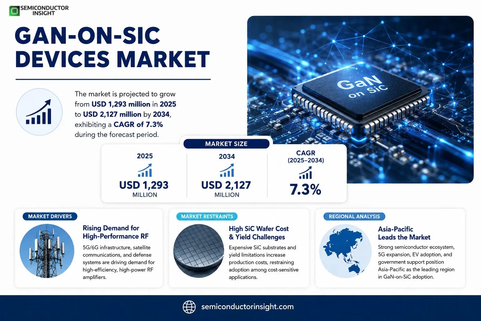
GaN-On-SiC Devices market was valued at USD 1,293 million in 2025 and is forecasted to reach USD 2,127 million by 2034, delivering a CAGR of 7.3% over the forecast horizon.
GaN-on-SiC devices comprise RF, microwave and mmWave components built on semi‑insulating silicon‑carbide substrates where a GaN/AlGaN heterostructure is grown primarily by MOCVD. The scope includes discrete GaN HEMT power transistors (die or packaged), monolithic microwave integrated circuits (MMICs) that integrate PA, driver, LNA or switch functions, and system‑level chips used inside power‑amplifier and transmit/receive modules. This architecture exploits GaN’s high breakdown voltage and current density together with SiC’s superior thermal conductivity, enabling higher efficiency and smaller die footprints for high‑output‑power applications.
MARKET DRIVERS
Enhanced Power Density
Manufacturers are gravitating toward GaN-on-SiC architectures because they deliver twice the power density of conventional silicon counterparts. This leap enables compact power modules that occupy less board space, a critical advantage for electric‑vehicle inverters and aerospace power supplies where weight and volume are premium constraints.
Thermal Management Advantages
The SiC substrate acts as an efficient heat sink, allowing devices to operate at higher junction temperatures without compromising reliability. The resulting reduction in cooling system complexity translates into lower bill‑of‑materials and shorter time‑to‑market for high‑performance applications.
➤ Industry surveys reveal that design teams cite thermal headroom as the top factor when selecting GaN‑on‑SiC for next‑generation converters.
As telecom operators upgrade to 5G and beyond, the demand for robust RF amplifiers that can sustain intense signal loads is rising. GaN‑on‑SiC amplifiers meet this need while maintaining linearity, positioning the GaN‑On‑SiC Devices Market as a strategic enabler for emerging network infrastructure.
MARKET CHALLENGES
Cost Competitiveness
The initial outlay for SiC wafers remains substantially higher than bulk silicon, pressing OEMs to justify the investment through lifecycle savings. While performance gains are clear, many midsize firms hesitate to re‑tool production lines without a demonstrable return horizon.
Other Challenges
Supply‑Chain Volatility
shortages of high‑purity SiC substrates have introduced lead‑time uncertainties. OEMs that depend on just‑in‑time inventories face scheduling disruptions, prompting a search for diversified sourcing strategies.
MARKET RESTRAINTS
Manufacturing Yield Limitations
Yield gaps stem from defect densities intrinsic to SiC crystal growth. Even minor imperfections can cascade into device failure, elevating scrap rates and inflating unit costs. Until yield improvements become industry‑standard, scaling production will remain constrained.
MARKET OPPORTUNITIES
Expansion into Renewable Energy Converters
Solar‑to‑grid inverters and offshore wind converters demand converters that can tolerate harsh environments while delivering high efficiency. GaN‑on‑SiC devices can reduce conversion losses and extend service intervals, creating a compelling value proposition for project developers seeking lower operational expenditures.
GaN-On-SiC Devices Market Trends
Thermal Management and Wafer‑Scale Cost Levers
The industry’s move from 100 mm to 150 mm SiC substrates is reshaping the cost structure of GaN‑On‑SiC devices. Larger wafers raise the per‑die silicon‑carbide material expense but spread fixed fab overhead across more units, delivering a measurable dip in unit price for high‑power RF transistors. At the same time, engineers are exploiting SiC’s superior thermal conductivity to push breakdown voltages higher, allowing designers to shrink die footprints while maintaining output power. The combination of reduced thermal resistance and smaller silicon footprint translates into lighter, more efficient modules for base‑station amplifiers and aerospace radar. Customers value the reliability gains that come from lower hotspot temperatures, prompting a shift toward designs that prioritize thermal path optimization over raw voltage headroom.
Other Trends
Application Migration Toward High‑Power Satellite and Radar Systems
Telecommunications operators and defense contractors are allocating more budget to satellite constellations and phased‑array radars that operate in the millimeter‑wave band. These platforms demand amplifiers capable of delivering tens of watts of output with minimal distortion, a niche where the GaN‑On‑SiC stack excels because the high‑frequency performance of GaN meets the thermal handling advantage of SiC. As satellite payloads become more compact, manufacturers are integrating GaN‑On‑SiC MMICs directly into transceiver modules, reducing the number of discrete components and simplifying the overall system architecture. This integration yields faster time‑to‑market for new frequency bands and supports the aggressive latency targets set by emerging broadband satellite services.
Supply‑Chain Consolidation and Platform Focus
Recent transactions have concentrated the upstream SiC substrate market, with a few players now controlling the majority of high‑purity wafers. This concentration is encouraging coordinated R&D efforts aimed at standardizing 150 mm processes, which in turn eases the entry barrier for smaller RF foundries. Parallel to this, major system integrators are defining reference platforms that pair specific GaN‑On‑SiC device families with defined packaging and test flows. By locking in a common platform, OEMs can achieve predictable performance across multiple generations, lower engineering change costs, and accelerate volume production. The net effect is a more resilient supply chain that can respond promptly to spikes in demand from both commercial telecom upgrades and defense procurement cycles.
COMPETITIVE LANDSCAPEKey Industry Players
Competitive Dynamics in the GaN‑On‑SiC Devices Market
Wolfspeed, now operating as a pure‑play SiC specialist after divesting its RF unit, continues to dominate the high‑power segment by leveraging deep expertise in semi‑insulating SiC substrates and mature MOCVD epitaxy. The company’s ability to supply 150‑mm wafers at competitive yields gives it a cost advantage that forces smaller IDM‑focused players to partner with dedicated foundries. Qorvo and NXP have each built integrated GaN‑on‑SiC design houses that couple RF system engineering with silicon carbide thermal management, allowing them to capture a sizable share of the telecom‑infrastructure and satcom pipelines where volume and reliability matter most. The market structure therefore resembles a tiered ecosystem: substrate suppliers at the base, a handful of vertically integrated IDM/foundry hybrids in the middle, and a ring of niche RF foundries that specialize in custom MMICs for defense and aerospace programs.Beyond the dominant tier, a diverse set of niche players sustains innovation in specialized application spaces. MACOM’s acquisition of Wolfspeed’s former RF portfolio enables it to offer turnkey GaN‑on‑SiC power amplifiers for radar and electronic‑warfare platforms, while RFHIC focuses on low‑loss, high‑linearity LNA modules for next‑generation 5G/6G base stations. Dynax Semiconductor and Mitsubishi Electric target high‑frequency millimeter‑wave markets, emphasizing wafer‑scale integration to shrink module footprints. Chinese entities such as CETC 55, Youjia Technology (Suzhou) Co., Ltd, and Shenzhen Taigao Technology are expanding their MOCVD capacity toward 200‑mm diameters, positioning themselves as cost‑effective alternatives for emerging regional defense contracts. The presence of defense giants like Raytheon Technologies and Northrop Grumman, which often outsource to these specialized foundries, underscores the strategic importance of maintaining a broad supplier base capable of meeting stringent reliability specifications.
List of Key GaN‑On‑SiC Devices Companies Profiled
- Sumitomo Electric Device Innovations (SEDI)
- MACOM
- Qorvo
- NXP
- RFHIC Corporation
- Raytheon Technologies
- Dynax Semiconductor
- Mitsubishi Electric
- CETC 55
- Northrop Grumman
- Ampleon
- UMS RF
- CETC 13
- ReliaSat (Arralis)
- WAVICE Inc
- Microchip Technology
- Youjia Technology (Suzhou) Co., Ltd
- Shenzhen Taigao Technology
- Hebei Sinopack Electronic Technology
Segment Analysis:
| Segment Category | Sub-Segments | Key Insights |
| By Type |
|
GaN HEMTs are favored for ultra‑high‑power density requirements. • Their 2DEG channel delivers superior breakdown voltage and current density. • Enables compact die footprints while maintaining high efficiency. • Drives innovation in radar and high‑gain transmitter modules. |
| By Application |
|
Telecom Infrastructure anchors demand for high‑frequency, high‑linearity power amplifiers. • Supports evolving 5G/6G antenna arrays requiring dense power delivery. • Benefits from the low RF loss of SiC substrate, enhancing overall network efficiency. • Provides a stable platform for massive‑MIMO deployments. |
| By End User |
|
Network Operators prioritize reliability and thermal robustness for base‑station upgrades. • GaN‑on‑SiC devices enable longer lifetimes under continuous high‑power operation. • Facilitate smoother integration with existing RF front‑end architectures. • Encourage adoption of advanced beam‑forming techniques. |
| By Wafer Size |
|
6‑inch wafers dominate current high‑volume production. • Offer a balance between yield improvement and equipment investment. • Enable cost‑effective scaling of MMIC families. • Serve as a stepping stone toward larger 8‑inch platforms. |
| By Thermal Management Strategy |
|
Advanced Heat‑Spreader Designs are critical for maintaining performance at extreme power densities. • Leverage SiC’s superior thermal conductivity to dissipate hotspots. • Reduce device derating and extend operational life. • Align with emerging high‑frequency radar and satellite payload requirements. |
Regional Analysis: GaN-On-SiC Devices Market
Asia-Pacific
China’s expansion of 4‑inch SiC wafer capacity has lowered entry barriers for local designers, enabling smaller firms to prototype GaN‑On‑SiC devices without relying on overseas sources. This localized substrate ecosystem shortens lead times and creates pricing flexibility that directly benefits end‑product manufacturers in automotive and renewable‑energy sectors.
OEMs in Japan and South Korea have integrated GaN‑On‑SiC converters into next‑generation on‑board chargers, citing superior thermal performance that allows higher charge rates without compromising battery longevity. This design shift is reshaping supplier contracts and prompting Tier‑1s to re‑evaluate their component road‑maps.
The rollout of millimeter‑wave base stations across dense urban clusters in India and Southeast Asia demands compact amplifiers capable of handling high peak power. GaN‑On‑SiC devices meet these specifications, prompting network operators to prioritize vendors that can deliver integrated solutions with reduced footprint.
High‑end smartphones and wearables in the region are experimenting with GaN‑On‑SiC power‑management ICs to extend battery life while supporting fast‑charging protocols. Early adopters report measurable gains in charge efficiency, prompting larger manufacturers to explore pilot programs.
North America
In the United States, defense contractors are the primary catalyst for the GaN‑On‑SiC Devices Market, seeking rugged power amplifiers that survive extreme thermal cycles. Parallel to defense spending, Silicon Valley start‑ups are targeting data‑center power‑delivery architectures that require high‑efficiency DC‑DC conversion. The regulatory climate encourages adoption of energy‑saving technologies, nudging large hyperscale cloud providers toward hybrid solutions that blend GaN speed with SiC durability. Consequently, investment in domestic wafer‑fab capacity is gaining momentum, although supply constraints keep the region dependent on Asian substrates for volume production.
Europe
European manufacturers are capitalising on stringent emissions legislation to embed GaN‑On‑SiC modules in electric‑bus traction drives. German automotive giants, in particular, are co‑funding joint‑venture labs that assess reliability under continental climate stressors. Additionally, the EU’s Horizon programmes allocate grants toward next‑generation wireless backhaul, where the high‑frequency performance of GaN combined with SiC’s thermal handling offers a compelling value proposition. These policy‑driven incentives are reshaping procurement strategies across the automotive and telecom supply chains.
South America
Brazil’s renewable‑energy expansion, especially in large‑scale solar farms, has opened a niche for high‑voltage converters that can operate with minimal cooling infrastructure. Local utilities are experimenting with GaN‑On‑SiC inverters to improve grid‑integration efficiency, despite the region’s limited domestic wafer production. Partnerships with Asian fab houses are therefore critical, and they are prompting Brazilian firms to develop application‑specific designs that align with regional climate and grid code requirements.
Middle East & Africa
In the Gulf Cooperation Council, the drive toward carbon‑neutral desalination plants has sparked interest in power‑electronics platforms that can survive high ambient temperatures. GaN‑On‑SiC devices, with their superior thermal conductivity, are being evaluated for motor‑drive systems in large‑scale water‑treatment facilities. Meanwhile, South‑African telecom operators are upgrading backhaul networks to support growing mobile‑data traffic, where compact, high‑power RF amplifiers present a cost‑effective upgrade path. Collaborative projects with European research institutes are helping to bridge the technology‑adoption gap in the region.
Report Scope
This market research report provides a comprehensive analysis of the GaN-On-SiC Devices Market , covering the forecast period 2026–2034. It offers detailed insights into market dynamics, technological advancements, competitive landscape, and key trends shaping the industry.
Key focus areas of the report include:
- Market Overview: The report begins with an overview outlining its current market scenario, key growth indicators, and industry transformation drivers. It discusses macroeconomic factors, demand–supply balance, regulatory landscape, and the strategic role of semiconductors in powering advancements across industries such as automotive, telecommunications, consumer electronics, and industrial automation.
- Market Size & Forecast: Historical data and future projections for revenue, unit shipments, and market value across major regions and segments.
- Segmentation Analysis: Detailed breakdown by product type, technology, application, and end-user industry to identify high-growth segments and investment opportunities.
- Regional Insights: Insights into market performance across North America, Europe, Asia-Pacific, Latin America, and the Middle East & Africa, including country-level analysis where relevant.
- Competitive Landscape: Profiles of leading market participants, including their product offerings, R&D focus, manufacturing capacity, pricing strategies, and recent developments such as mergers, acquisitions, and partnerships.
- Technology Trends & Innovation: Assessment of emerging technologies, integration of AI/IoT, semiconductor design trends, fabrication techniques, and evolving industry standards.
- Market Drivers & Restraints: Evaluation of factors driving market growth along with challenges, supply chain constraints, regulatory issues, and market-entry barriers.
- Stakeholder Insights: Insights for component suppliers, OEMs, system integrators, investors, and policymakers regarding the evolving ecosystem and strategic opportunities.
Primary and secondary research methods are employed, including interviews with industry experts, data from verified sources, and real-time market intelligence to ensure the accuracy and reliability of the insights presented.
FREQUENTLY ASKED QUESTIONS:
What is the current market size of GaN-On-SiC Devices Market?
-> GaN-On-SiC Devices Market was valued at USD 1,293 million in 2025 and is expected to reach USD 2,127 million by 2034, at a CAGR of 7.3% during the forecast period.
Which key companies operate in GaN-On-SiC Devices Market?
-> Key players include Sumitomo Electric Device Innovations (SEDI), MACOM, Qorvo, NXP, RFHIC Corporation, Raytheon, Dynax Semiconductor, Mitsubishi Electric, CETC 55, Northrop Grumman, Ampleon, UMS RF, CETC 13, ReliaSat (Arralis), WAVICE Inc, Microchip Technology, Youjia Technology (Suzhou) Co., Ltd, Shenzhen Taigao Technology, Hebei Sinopack Electronic Technology.
What are the key growth drivers?
-> Key growth drivers include defense and satellite communications expansion, high‑bandwidth 5G/6G RF architecture demand, need for ultra‑high power‑density and reliability, and advances in SiC substrate scaling.
Which region dominates the market?
-> Asia dominates the market, driven by strong demand in wireless infrastructure, satellite communications, and aerospace & defense applications.
What are the emerging trends?
-> Emerging trends include wafer‑size scaling from 100 mm to 150 mm (6‑inch) and toward 200 mm, RF business consolidation such as Wolfspeed’s sale to MACOM, and expanding adoption of GaN‑on‑SiC for ultra‑high‑power 5G/6G applications.
Get Sample Report PDF for Exclusive Insights
Report Sample Includes
- Table of Contents
- List of Tables & Figures
- Charts, Research Methodology, and more...
 Download Sample Report PDF