Key Statistics
Key Takeaways
- Market trajectory: worldwide device sales amount to USD 1,293.0 million in 2025 and are expected to approach USD 2,127.0 million by 2034, implying a 5.7% annual increase as compound-semiconductor amplifiers extend into higher-power radio infrastructure and advanced sensing.
- Discrete RF GaN transistors retain an estimated ~58% market share because packaged HEMTs serve high-output transmit chains; GaN MMICs contribute ~42%, with growing requirements for integrated gain stages, switching functions and space-efficient radar and satellite modules.
- Telecommunications infrastructure represents around ~43% of applications; aerospace and defense contribute ~33%, satellite communications ~16% and other specialist microwave uses ~8%. Engineering performance is measured at the relevant radio band rather than by wattage in isolation.
- Asia-Pacific leads with an estimated ~38% share through electronic systems production and radio deployments, compared with North America ~32% and Europe ~23%; US defense design and European RF foundries remain critical competitive centers.
- Technology choice favors GaN-on-SiC for an estimated ~72% of revenue where thermal paths and radar-grade power matter; GaN-on-Si covers roughly ~28% through cost-sensitive process opportunities, although actual qualification depends on channel temperature and defect reliability.
RF GaN Devices Market Overview
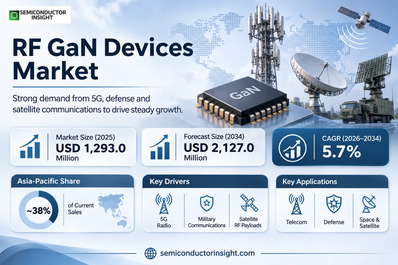
RF GaN devices market was valued at USD 1,293.0 million in 2025 and is forecast to reach USD 2,127.0 million by 2034, equivalent to a CAGR of 5.7% over 2026–2034. Asia-Pacific accounts for an estimated ~38% of current sales, with military communications, 5G radio equipment and satellite RF payloads shaping adoption worldwide.
RF gallium-nitride devices exploit the high electric-field tolerance and carrier density of GaN heterostructures to create compact, efficient power amplification at radio and microwave frequencies. Most commercial products are high-electron-mobility transistors, or HEMTs, rather than conventional silicon MOSFETs. Sales comprise discrete RF GaN transistor dies and packages, GaN monolithic microwave integrated circuits, and eligible integrated power-amplifier or driver assemblies within the specified product family.
The substrate selection is commercially important. GaN-on-SiC uses the thermal performance of silicon carbide to support demanding radar, satellite and defense transmitters. GaN-on-Si can exploit scalable semiconductor wafer production and potentially lower material costs for selected infrastructure devices. Neither substrate automatically guarantees higher efficiency; channel temperature, defect density, RF linearity and package impedance determine whether a candidate part will pass its customer-specific qualification.
At the product level, Qorvo offers a DC–2.7 GHz GaN-on-SiC discrete device in a compact package and a separate 500 W rated family targeted at 1.2–1.4 GHz radar. MACOM catalogs integrated GaN amplifiers with operating windows reaching into X-band and Ka-band, including a 125 W radar MMIC. Such examples demonstrate discrete and integrated architectures, with stated outputs tied to particular test frequencies and power levels.
RAN equipment manufacturers increasingly optimize not just peak transmit power but linearity across a wide modulated signal envelope. In a massive-MIMO antenna, many amplifier paths share the coverage objective, making package size and thermal load important system costs. Defense radar designers instead emphasize pulsed output, long-term operation and robust power cycling in active arrays. Satellite designers may prioritize payload weight and controlled performance in demanding orbital environments.
Foundry access influences how specialized RF GaN markets develop. United Monolithic Semiconductors provides GH15 and GH25 processes and advertises 2026 shared wafer runs, allowing smaller microwave designers to prototype without owning an entire epitaxy line. Qorvo reported a substantial X-band power-density milestone under a US research program in September 2026, demonstrating continuing technical activity while leaving actual customer production timing subject to qualification and contracting.
Segment Analysis: By Type
Discrete RF GaN Transistors account for an estimated ~58% of 2025 sales through device-level purchases for radar, radio and power amplifier boards, while GaN MMICs contribute ~42% and combine multiple RF stages on a single chip. The integrated category can include driver, power amplifier, low-noise and switching functions when they are part of the stated GaN RF device offering, avoiding addition of unrelated complete radar systems.
| Type | Function | Market position |
|---|---|---|
| Discrete RF GaN Transistors | A GaN HEMT die or packaged transistor provides a high-power gain element that an RF system designer matches externally to the target frequency and supply voltage. Qorvo offers devices ranging from about 15 W in compact input-matched radio packages to a 500 W class radar transistor, illustrating a wide application spectrum. | An estimated ~58% type share reflects numerous power-stage sockets that use a separate transistor, although the nominal output power of each part varies with test conditions. |
| GaN MMICs | Monolithic microwave integrated circuits place multiple high-frequency active and passive structures on one semiconductor die, allowing designers to optimize gain stages, matching networks and controls together. MACOM lists 125 W X-band radar power amplifiers and GaN devices spanning several microwave bands, providing evidence for sophisticated integrated offerings. | The estimated ~42% share grows as radar arrays and satellite systems seek smaller footprints, but full equipment cabinets and non-GaN receiver electronics fall outside the category. |
Secondary segmentation
Additional commercial axes identify the purchasers, material platform and manufacturing route for eligible GaN RF chips. Mobile network operators lead end-user exposure at an estimated ~42%, GaN-on-SiC holds around ~72% by material configuration, and integrated device manufacturers account for ~55% by process platform. A single transaction can simultaneously belong to several axes without creating an additional device category or a separate downstream equipment sale.
| Axis | Members | Commercial role |
|---|---|---|
| End User | Mobile Network Operators; Defense Contractors; Equipment Integrators | Network operators specify radio-site performance; defense customers require rugged repeatable radar power; integrators select exact chip, matched package and qualification documents. |
| Technology | GaN-on-SiC; GaN-on-Si | SiC substrates improve heat conduction for high-power RF; silicon substrates offer cost and wafer-scale advantages where device performance and reliability remain sufficient. |
| Process Platform | Integrated Device Manufacturers (IDMs); Specialty RF Foundries; Fabless Design Houses | IDMs control fabrication and product roadmaps; foundries provide qualified GaN HEMT processes; fabless designers bring application-specific MMIC layouts to external lines. |
Segment Analysis: By Application
Telecom Infrastructure captures an estimated ~43% of demand, Aerospace & Defense ~33%, Satcom ~16% and other specialized RF applications ~8%. Each sector chooses differently between discrete high-current GaN HEMTs and integrated microwave MMICs, with the intended frequency, spectral purity and operating duty more decisive than the nominal semiconductor output-power rating.
| Application | Demand characteristics |
|---|---|
| Telecom Infrastructure | GaN power devices serve radio amplifier stages in base-station and other fixed wireless infrastructure where efficient output and strong linearity help manage network operating expense. Qorvo describes a QPD0060 type part for Doherty amplifier architectures, illustrating a practical link between transistor design and radio output stages. This application represents an estimated ~43% of sales; network deployment figures remain context rather than a direct measure of chip revenue, and not every radio uses GaN at its final amplifier. |
| Aerospace & Defense | Radar arrays and electronic warfare systems use concentrated RF transmit power to detect signals, illuminate targets or transmit across challenging spectrum conditions. GaN-on-SiC is attractive where thermal conductivity and output density support smaller active modules. A 125 W X-band MMIC from MACOM exemplifies the component class, while Qorvo offers higher-power discrete devices for other bands. The estimated ~33% market share depends on qualified defense production and test programs rather than the entire military procurement budget. |
| Satcom | Satellite payloads, phased-array ground terminals and broadband microwave links require high-efficiency gain at specific uplink or downlink frequencies. GaN MMICs can reduce board-level assembly steps and package mass, but radiation tolerance, noise performance and spacecraft thermal design remain subject to individual flight qualification. Satcom contributes an estimated ~16% of 2025 value and can grow through new space networks, although spacecraft sales and subscription revenue are not equivalent to RF device shipments. |
| Others | Scientific microwave instruments, high-power test equipment and specialized industrial radio sources account for an estimated ~8% of the category. Device choice is often made after load-pull testing because a 15 W input-matched GaN device and a 500 W radar HEMT have very different impedance, heat and linearity requirements. These applications create differentiated niches for foundries and smaller RF designers, but the category excludes unrelated high-voltage GaN power switches used only for low-frequency electrical conversion. |
A ground radar phased array and a multicarrier cellular radio cabinet may both use GaN, but they stress their chips differently. Radar selects pulsed saturation, duty cycle and heat spreading at its band, while telecom designs place extra emphasis on linearized modulated power and long-term energy cost. The application split is therefore best understood as an engineering demand map supported by exact product specifications, not as a single interchangeable RF amplifier market.
Regional Analysis
Asia-Pacific has the largest estimated share of RF GaN device purchases at ~38%, supported by manufacturing ecosystems, radio network upgrades and defense electronics investment. North America follows at ~32%, with semiconductor design and radar engineering; Europe represents ~23% through industrial RF foundries and aerospace system integrators. South America holds roughly ~4%, and the Middle East and Africa ~3%, with much of their demand supplied by global component manufacturers.
Which regions combine radio infrastructure investment with specialized GaN engineering?
The geographic sales pattern reflects both where RF devices are incorporated into equipment and where the completed amplifiers are finally installed. Asia supplies many electronic assemblies for world markets, while US-based GaN developers support defense radar programs and European foundries support a range of outsourced designs. The substrate technology, export permissions and availability of specialized testing differ by country, preventing identical procurement assumptions across the five regions.
| Region | Position | Growth outlook | Demand profile | What decides supplier selection |
|---|---|---|---|---|
| Asia-Pacific | Largest (~38%) | Expanding (~6.4% CAGR) | Radio equipment fabrication, radar and communications systems | RF foundry yield and qualified thermal packaging |
| North America | Second (~32%) | Growing (~5.6% CAGR) | Defense radar, phased arrays and GaN design | Export qualification and heat dissipation |
| Europe | Third (~23%) | Growing (~5.1% CAGR) | Specialty MMIC foundries, space and aerospace electronics | Process design kits and reliability testing |
| South America | Smaller (~4%) | Selective (~4.8% CAGR) | Telecom upgrades and specialized radar demand | Imported amplifier parts and technical support |
| Middle East & Africa | Smaller (~3%) | Selective (~2.5% CAGR) | Satellite links, defense radio and mobile networks | Environmental qualification and international sourcing |
Key RF GaN Devices Manufacturers and Competitive Landscape
The GaN RF supplier landscape spans vertically integrated producers, open semiconductor foundries and microwave chip designers. Qorvo sells discrete GaN-on-SiC transistors and integrated RF amplifier devices with detailed frequency characterization. MACOM supplies GaN MMICs and front-end assemblies, while UMS offers specialized foundry processes to third-party design teams. Defense prime contractors often specify devices within larger radar systems and should not automatically be treated as merchant GaN wafer vendors.
Qorvo offers several production GaN power transistors spanning compact 15 W parts through devices rated hundreds of watts at radar frequencies. Its QPD1013 is described as a 150 W GaN-on-SiC HEMT in a 7.2 by 6.6 millimeter plastic package, whereas a distinct QPD1003 is a 500 W internally matched transistor for 1.2–1.4 GHz operation. These products serve different RF impedance and thermal targets and cannot be treated as equivalent commodity pieces.
MACOM combines discrete transistor and GaN MMIC expertise, with a catalog of power amplifiers for applications from C-band through millimeter-wave services. Its June 2026 radar showcase included a 125 W X-band GaN MMIC intended for pulsed operation and a 50 W C-band front-end module. Those integrated products offer equipment designers ways to reduce separate board-level components, while raising the importance of package-level cooling and signal isolation.
United Monolithic Semiconductors sells access to qualified GaN-on-SiC foundry processes and design kits. Its GH25 technology targets high-power microwave applications around 20 GHz with 0.25 micrometer transistor gates, and GH10 extends process capability for higher-frequency MMICs. An outsourced wafer line can serve fabless customers that value application-specific circuits but lack capital to construct and qualify their own III-V compound-semiconductor fab.
Other suppliers and customers include RFHIC, Sumitomo Electric Device Innovations, defense radar integrators and small specialist microwave laboratories. Their commercial roles differ: a product maker may sell a packaged discrete HEMT, a foundry can fabricate wafer-level die for another designer, and a defense contractor purchases RF chips for integrated phased-array systems. Market participation requires component-level supporting evidence rather than treating every contractor as a separate GaN semiconductor merchant supplier.
Tier structure
| Tier | Companies | Basis of competition |
|---|---|---|
| Documented RF GaN product suppliers | Qorvo; MACOM | GaN-on-SiC HEMTs, RF transistor packages and microwave power-amplifier MMICs with detailed electrical specifications. |
| Open foundry and specialist process platforms | United Monolithic Semiconductors; selected RF foundries | GaN GH10, GH15 and GH25 process design kits, wafer runs and application-specific chip fabrication. |
| Additional supply and systems ecosystem | RFHIC; Sumitomo Electric Device Innovations; defense radar contractors | Specialized RF devices and downstream integration; production ownership and package evidence vary by product. |
Key companies profiled
- Qorvo
- MACOM
- United Monolithic Semiconductors
- RFHIC
- Sumitomo Electric Device Innovations
- Northrop Grumman
RF GaN Devices Production Capacity Analysis
RF GaN device capacity is constrained by epitaxial quality, HEMT process control, wafer-level yield, high-frequency testing and RF package assembly. Producing a useful chip requires uniform GaN heterostructures and precise gate definition, followed by passivation, interconnect metallization and high-power characterization. A foundry’s quoted wafer diameter or transistor gate size does not alone indicate the number of qualified packaged radar amplifiers available for shipment.
GaN-on-SiC process flows use a silicon-carbide substrate and specialized nitride epitaxy to form a high-mobility electronic channel. Wafer screening is necessary to control trapping, breakdown behavior and dispersion under high electric fields. UMS lists GH25 parameters including a 0.25 micrometer gate, 100 millimeter wafer diameter and roughly 5 W/mm power density under its specific design conditions. A fabless customer can utilize these capabilities only after appropriate mask, layout and model verification.
Integrated microwave circuits demand strong isolation between active devices, passive transmission lines and bias networks. Foundry tools must support accurate metal thicknesses and through-substrate vias to manage loss and parasitics as the frequency rises. MACOM and Qorvo packages then transfer heat from concentrated power density into flanges or boards; test teams verify gain, output and stability at the stated band. A transistor that functions in continuous wave may behave differently in a high-peak pulsed radar.
Production supply depends on more than lithography equipment. Export-control compliance, qualified substrate suppliers, hermetic or overmolded packages and specialized load-pull laboratories can affect lead times for defense-grade parts. Open foundry multi-project wafer programs lower entry costs for proof-of-concept designs but do not remove lengthy aerospace or military testing. Customers also require lot traceability and controlled process revisions before approving a GaN transistor for multi-year deployment.
RF GaN Devices Market Dynamics: Drivers, Restraints and Opportunities
Growth reflects high-output wireless radios, array radar, satellite links and broader access to specialized compound-semiconductor foundries. The advantages of GaN power density must be weighed against fabrication cost and thermal reliability under actual microwave loading. Advanced GaN-on-SiC processes serve premium radar and aerospace equipment, while GaN-on-Si may improve economics for selected infrastructure frequency bands when qualification requirements can be met.
MARKET DRIVERS
Drivers Impact Analysis*
| Market Drivers | Impact Rank | CAGR Contribution (%) | 2026–2028 | 2029–2031 | 2032–2034 |
|---|---|---|---|---|---|
| 5G massive-MIMO and radio upgrade requirements | High | +3.40% | High | High | Medium |
| Defense radar and electronic warfare modernization | High | +2.80% | High | High | High |
| High-efficiency satellite communications amplifiers | Medium-High | +2.10% | Medium | High | High |
| GaN MMIC integration and package miniaturization | Medium | +1.80% | Medium | High | High |
| Open RF foundries and wafer process access | Low-Medium | +1.10% | Medium | Medium | High |
| Others (industrial microwave research adoption) | Low | +0.60% | Low | Medium | Medium |
Radio equipment seeks effective power across many signal paths
A massive-MIMO base station may incorporate dozens of independent RF amplification channels that together determine coverage and energy use. GaN devices can offer suitable saturated power and efficient operation when the circuit supports the required linearity. Qorvo products document the use of GaN transistors in Doherty amplifier arrangements, showing a defined technology path. Network capital spending is still an indirect demand signal, not a count of finished GaN chips.
Modern phased-array radar imposes stringent microwave demands
Active radar arrays need repeatable transmitter elements with adequate output, controlled phase and reliable duty performance. MACOM has published a 125 W X-band MMIC serving pulsed radar designs, and Qorvo has demonstrated high-power discrete GaN HEMTs for other frequency bands. The components offer size and efficiency benefits when integrated properly, but system builders demand thermal characterization and supplier process stability before beginning high-volume installation.
Satellite communications reward compact high-frequency gain
Space platforms and terrestrial satcom terminals place a premium on high power per unit mass, linearity and reliable microwave output. GaN MMICs can reduce the number of separately matched components along the amplifier chain. Qualification differs between a satellite payload and a ground terminal because the spacecraft faces launch stress and radiation exposure. These additional requirements create opportunities for specialist foundry and package technology rather than universal acceptance of every new GaN transistor.
Integrated microwave chips simplify portions of the RF front end
A GaN monolithic circuit can integrate active amplification with passive matching and switching elements, reducing some board-level RF interconnections and potentially improving reproducibility. MACOM product listings include C-band and X-band modules alongside multi-stage MMICs, illustrating the range of equipment architectures supported. The benefit depends on the total design, as a combined transmitter and receiver package may need special isolation and enhanced thermal spreading.
Accessible process design kits enable more specialized devices
Fabless microwave engineers can use published GaN HEMT models to optimize an amplifier before purchasing physical wafer space. UMS offers 2026 shared foundry runs for GH10, GH15 and GH25 technologies, allowing smaller design groups to test circuits at defined process nodes. This improves experimentation capacity while still requiring electrothermal simulation and actual load-pull verification. New mask runs and qualification can remain expensive for low-volume satellite or defense projects.
MARKET RESTRAINTS
Restraints Impact Analysis*
| Market Restraints | Impact Rank | CAGR Contribution (%) | 2026–2028 | 2029–2031 | 2032–2034 |
|---|---|---|---|---|---|
| High epitaxy, substrates and manufacturing costs | High | -2.10% | High | Medium | Medium |
| Thermal and trapping reliability engineering | Medium-High | -1.70% | High | High | High |
| Defense qualification and export restrictions | Medium | -1.40% | Medium | High | High |
| Others (silicon LDMOS and competing RF designs) | Low | -0.90% | High | Medium | Low |
Wafer defects and RF packaging can make GaN costly
High-quality GaN-on-SiC wafers require specialized epitaxy and defect controls before a HEMT is manufactured. When the circuit also contains high-frequency passives and complex packaging, a sophisticated MMIC may be more expensive than a mature lower-frequency silicon alternative. GaN-on-Si can offer a manufacturing route with different costs, but substrate choice must satisfy thermal and electrical performance. Lower wafer cost does not always deliver a cheaper qualified amplifier assembly.
High power density creates demanding thermal conditions
Gallium-nitride devices can concentrate significant heat in a small channel region even when their power-added efficiency is favorable. Excess temperature and charge trapping can affect gain, output and long-term reliability, so designers simulate electrothermal behavior and test under duty cycles representative of the field. Qorvo’s X-band thermal research highlights the challenge. Component specifications at a single laboratory temperature cannot guarantee continuous radar performance in a sealed outdoor enclosure.
Defense and satellite approval delays procurement
High-reliability RF semiconductors may be required to meet mission-specific radiation, vibration, operational lifetime and process-traceability conditions. Certain transistor exports also require authorization, adding cost and project uncertainty. A newly demonstrated high-frequency GaN MMIC cannot be shipped directly into an aircraft radar without suitable qualification. Equipment builders therefore maintain approved supplier and part lists, limiting how quickly product announcements translate into recognized component revenue.
Other amplifier technologies remain commercially attractive
Established silicon LDMOS retains cost and maintenance advantages in several communications and industrial frequency bands, while GaAs technology can provide appropriate gain or low-noise characteristics in some receiver paths. A complete radio front end may combine materials rather than use GaN everywhere. GaN providers must demonstrate actual system-level power, linearity and temperature performance to justify a design change when competing semiconductors already meet an OEM customer’s requirements.
MARKET OPPORTUNITIES
Compact X-band radar transmit modules
GaN MMICs designed for 8–12 GHz radar systems can reduce interconnection complexity and deliver substantial pulsed output in a known package. MACOM announced a 125 W X-band device for those applications, while other suppliers provide high-power HEMTs for band-specific architectures. System engineers may reduce amplifier count or heat-spreader mass, but each design must still meet array phase, cooling and pulse-response constraints.
Higher-frequency MMICs via advanced GaN foundries
UMS describes a 0.1 micrometer GH10 process supporting RF applications toward 60 GHz, potentially opening integrated transmit functions in higher-frequency communications and sensing. Foundry offerings can help specialist designers develop such circuits without owning semiconductor production equipment. Customer adoption depends on real-world power gain, wafer yield, design-kit accuracy and the ability to integrate a usable package rather than the process node alone.
Rugged RF amplification for satellite ground stations
Ground terminals serving new satellite constellations can benefit from efficient microwave uplink stages, especially where a small enclosure must deliver stable RF output in difficult weather. A GaN power MMIC can improve power density in a compatible antenna system. Providers will need to support specialized connector, board and cooling requirements, with component purchases distinguished from the much larger commercial value of satellite communication services.
Thermal research becomes differentiated product performance
Defense-led device research into reducing transistor thermal resistance can enable higher usable RF output in dense radar arrays. Qorvo reported a large X-band power-density improvement under DARPA-sponsored work in September 2026. Further opportunities involve translating test milestones into reproducible wafer processing and package performance for customers. The value arises only after qualification and procurement, rather than from the laboratory result by itself.
RF GaN Devices Supply Chain Analysis
RF GaN supply begins with qualified silicon-carbide or silicon substrates, nitride epitaxy and HEMT fabrication, followed by wafer probing, specialized microwave packaging and frequency-specific RF characterization. Integrated device manufacturers and contract foundries supply discrete chips and MMICs to amplifier makers and system integrators. The latter install devices into radar, satellite or telecom equipment, with chip-market value remaining separate from the selling price of a whole phased array, base station or spacecraft.
Materials. Gallium nitride epitaxy requires precise crystal composition and defect management to obtain repeatable channel behavior at the intended radio frequency. Silicon-carbide substrates support strong heat extraction, while silicon platforms can offer different wafer cost advantages. A transistor used for high-power radar needs stringent trapping, breakdown and leakage screening before circuit assembly. Raw substrate shipments do not count as completed RF GaN transistor or MMIC sales, and total gallium production is not equivalent to device-market revenue.
Production. A GaN MMIC foundry builds active transistor structures alongside thin-film resistors, capacitors and distributed microwave transmission lines. Process control and RF wafer probing establish gain and efficiency characteristics, while thermal attachment and package geometry determine installed performance. Specialized GaN HEMT process descriptions detail passive integration and loss control, but every finished chip must be screened at its intended operating band. Finished products also require thermal assembly and independent load-pull tests before a radar contractor can approve a high-power 125 W class amplifier.
Distribution. Some RF GaN products are bought directly from vertically integrated semiconductor companies, while fabless designers obtain wafers through specialty foundry agreements. Component suppliers provide application notes, models and evaluation boards to reduce design risk. Defense and aerospace customers may have additional export and process-traceability requirements. A part advertised as 500 W in one radar band cannot be substituted into an unrelated RF assembly without adjusting bias, matching and cooling.
Applications. A base-station maker combines GaN radio amplifier chips with antenna elements and software, while a radar contractor needs stable pulsed power across many active array elements. Ground satcom equipment adds different weather and duty-cycle requirements. The end user pays for complete electronic systems, but the semiconductor market concerns the eligible GaN dies, transistor packages and MMIC assemblies within them. Growth in terminal installations cannot be taken directly as a monetary estimate of GaN chip sales.
Recent Developments in the RF GaN Devices Market
- 22 September 2026 X-band GaN device thermal milestone
Qorvo announced more than a 400% improvement in transistor RF power density at X-band under a DARPA THREADS research program. The technical advance aimed to reduce channel heat limitations for next-generation radar, electronic warfare and communications applications. The disclosed result is a research achievement, not a verified annual output volume or a universal efficiency improvement across every commercial GaN process. Source - June 2026 Radar-focused integrated device demonstrations
MACOM disclosed multiple GaN amplifier prototypes and products at the 2026 International Microwave Symposium, including a 50 W C-band front-end module, a 16 W X-band module and a 125 W multi-stage GaN MMIC. The announcements identify actual frequency-band use cases and intended output performance for aerospace and defense designers. They also illustrate how integrated modules differ from discrete HEMT transistor packages. Source - July 2026 High-power S-band radar transistor preview
Qorvo published product information for the QPD2562L, a GaN-on-SiC transistor designed for approximately 2.5–3.3 GHz radar operation with output ratings of 200 W or more depending on band conditions. Its input pre-match simplifies some RF board design tasks, although full output matching and thermal testing remain necessary. A preview status should not be read as a confirmed volume-shipment program. Source - May 2026 Compact wideband GaN device documentation
Qorvo updated information for the QPD1013, a 150 W class GaN-on-SiC HEMT with a DC–2.7 GHz advertised range in a 7.2 by 6.6 millimeter DFN package. Its published test performance includes around 64.8% power-added efficiency at 1.8 GHz under the specified condition. That result applies to this particular transistor and should not be transferred to every radio-frequency GaN amplifier. Source - 2026 Open multi-project GaN wafer runs
United Monolithic Semiconductors listed 2026 shared foundry availability for GH10, GH15 and GH25 GaN HEMT technologies. The program provides a pathway for specialized RF designers to purchase wafer area and evaluate custom amplifiers without committing to a complete private fabrication line. Production qualification, process-design-kit access and customer-specific final packaging remain separate steps before broader commercial deployment. Source - March 2026 High-power low-GHz GaN transistor revisions
Qorvo released a revised datasheet for the QPD1016, a 500 W class 50 V GaN HEMT used in radar, avionics and test applications with a frequency range extending to 1.7 GHz. Published figures at 1.3 GHz include a gain near 23.9 dB and specified power-added efficiency. This product evidence reinforces demand for high-power discrete structures, distinct from integrated microwave chip modules. Source
REPORT SCOPE & SEGMENTATION
| Attribute | Details |
|---|---|
| Study Period | 2020–2034 |
| Base Year | 2025 |
| Estimated Year | 2026 |
| Forecast Period | 2026–2034 |
| Historical Period | 2020–2024 |
| Market Size 2025 | USD 1,293.0 million |
| Market Size 2026 | USD 1,366.5 million |
| Market Size 2034 | USD 2,127.0 million |
| Growth Rate | CAGR of 5.7% from 2026–2034 |
| Unit | Value (USD Million) |
| Segmentation | Type, Application, End User, Technology, Process Platform and Region |
| By Type | Discrete RF GaN Transistors · GaN MMICs |
| By Application | Telecom Infrastructure · Aerospace & Defense · Satcom · Others |
| By End User | Mobile Network Operators · Defense Contractors · Equipment Integrators |
| By Technology | GaN-on-SiC · GaN-on-Si |
| By Process Platform | Integrated Device Manufacturers (IDMs) · Specialty RF Foundries · Fabless Design Houses |
| By Region | Sales of eligible discrete RF GaN transistors, GaN MMIC chips and integrated GaN amplifier/driver modules Asia-PacificChina, Japan, South Korea North AmericaUnited States, Canada, Mexico EuropeFrance, Germany, United Kingdom South AmericaBrazil, Argentina, Chile Middle East & AfricaSaudi Arabia, United Arab Emirates, South Africa |
| Key Companies Profiled | Qorvo; MACOM; United Monolithic Semiconductors; RFHIC; Sumitomo Electric Device Innovations; Northrop Grumman |
| Customization Scope | Application frequency, GaN material substrate, HEMT process node, integrated MMIC functionality and supplier qualification can be examined for individual RF design programs. |
Frequently Asked Questions
What is the market size for RF GaN devices?
The global RF gallium-nitride device category accounted for USD 1,293.0 million in 2025 and is projected at USD 2,127.0 million by 2034, equivalent to a CAGR of 5.7% during 2026–2034. Revenue includes discrete GaN RF HEMTs, monolithic microwave integrated circuits and eligible integrated amplifier assemblies. It does not include complete telecom networks, military radar installations or satellite communication subscriptions.
What distinguishes a GaN HEMT from an RF silicon MOSFET?
A gallium-nitride high-electron-mobility transistor uses an electron channel formed at a semiconductor heterostructure, allowing strong electric fields and high power density in suitable microwave applications. Conventional silicon RF LDMOS devices use a different channel structure and frequently benefit from mature low-frequency manufacturing economics. Device choice must consider output power, linearity, actual frequency and cooling rather than assuming either material wins in every application.
Which device category currently sells the most?
Discrete RF GaN transistors hold an estimated ~58% of market value, while GaN MMICs account for around ~42%. Discrete HEMTs can give equipment developers flexibility to implement external matching and select their own amplifier architecture. MMICs integrate several high-frequency circuit elements on one chip, useful in space-constrained radar and satellite equipment. Both categories require accurate thermal characterization and RF measurements for the specified operating band.
What application is the largest?
Telecommunications infrastructure accounts for an estimated ~43% of 2025 demand, followed by aerospace and defense near ~33%, satellite communications about ~16% and other microwave applications ~8%. Mobile radio systems need efficient linear amplification, while radar relies on pulsed output and antenna-array precision. Satellite terminals add packaging and operating-lifetime constraints. The application mix excludes revenue from the finished ground station or network services.
Why is GaN-on-SiC an important platform?
Silicon carbide provides favorable thermal conduction under the GaN heterostructure, supporting high-power radar and aerospace transistors when the package is correctly designed. GaN-on-SiC is assigned an estimated ~72% share, with GaN-on-Si around ~28%. Silicon substrates can reduce fabrication cost for some infrastructure devices, but silicon also changes heat removal and material defects. The best choice depends on demonstrated reliability and target amplifier economics.
Which region has the highest demand?
Asia-Pacific leads with an estimated ~38% of RF GaN device revenue through radio equipment assembly and regional wireless activity. North America represents ~32%, with defense-related design and specialized semiconductor supply, while Europe holds ~23% through foundries and aerospace electronics. South America contributes around ~4%, and Middle East and Africa approximately ~3%. Device shipments can originate in one region while the finished radio is deployed in another.
How does GaN improve radar amplifier performance?
A suitable GaN HEMT can deliver high output power and efficiency in a compact die, allowing active electronically scanned arrays to use dense RF transmitter modules. MACOM offers a 125 W class X-band MMIC, while Qorvo catalogs hundreds-of-watts discrete HEMTs for other radar frequencies. These ratings apply at specified test points; array designers must still validate phase, switching timing, thermal management and the reliability of each integrated package.
What does an RF GaN specialty foundry offer?
An open semiconductor foundry provides qualified GaN HEMT fabrication, process design kits and wafer runs to outside microwave design teams. United Monolithic Semiconductors advertises GH25 and higher-frequency GH10 technologies, including multi-project wafer access. These services can reduce the capital needed to prototype a custom MMIC, but customers must complete RF testing, packaging, product qualification and commercial sourcing before a transistor is delivered to an equipment manufacturer.
What limits faster adoption of RF GaN devices?
Demand is constrained by compound-semiconductor wafer costs, epitaxial defects, channel heat, trapping behavior and lengthy defense or space qualification. Export controls can further restrict device availability for some end users. In other applications established silicon LDMOS or GaAs technology remains economical. Equipment makers are unlikely to change a proven amplifier solely because a new GaN part advertises high peak output without supporting data at the required frequency and duty cycle.
Which years and commercial dimensions are covered?
The analysis uses 2025 as the base year, 2026 as the estimate and 2034 as the forecast endpoint. Device types are discrete GaN transistors and MMICs, with telecom, defense, satellite and other applications. Additional classifications address mobile operators, defense contractors, integrators, GaN-on-SiC or silicon substrates, and IDM, foundry or fabless production structures. These represent different views of the same eligible RF semiconductor sales rather than separate cumulative markets.
Research Sources & Evidence Base
Get Sample Report PDF for Exclusive Insights
Report Sample Includes
- Table of Contents
- List of Tables & Figures
- Charts, Research Methodology, and more...
 Download Sample Report PDF