Super Junction MOSFET Wafer Market Insights
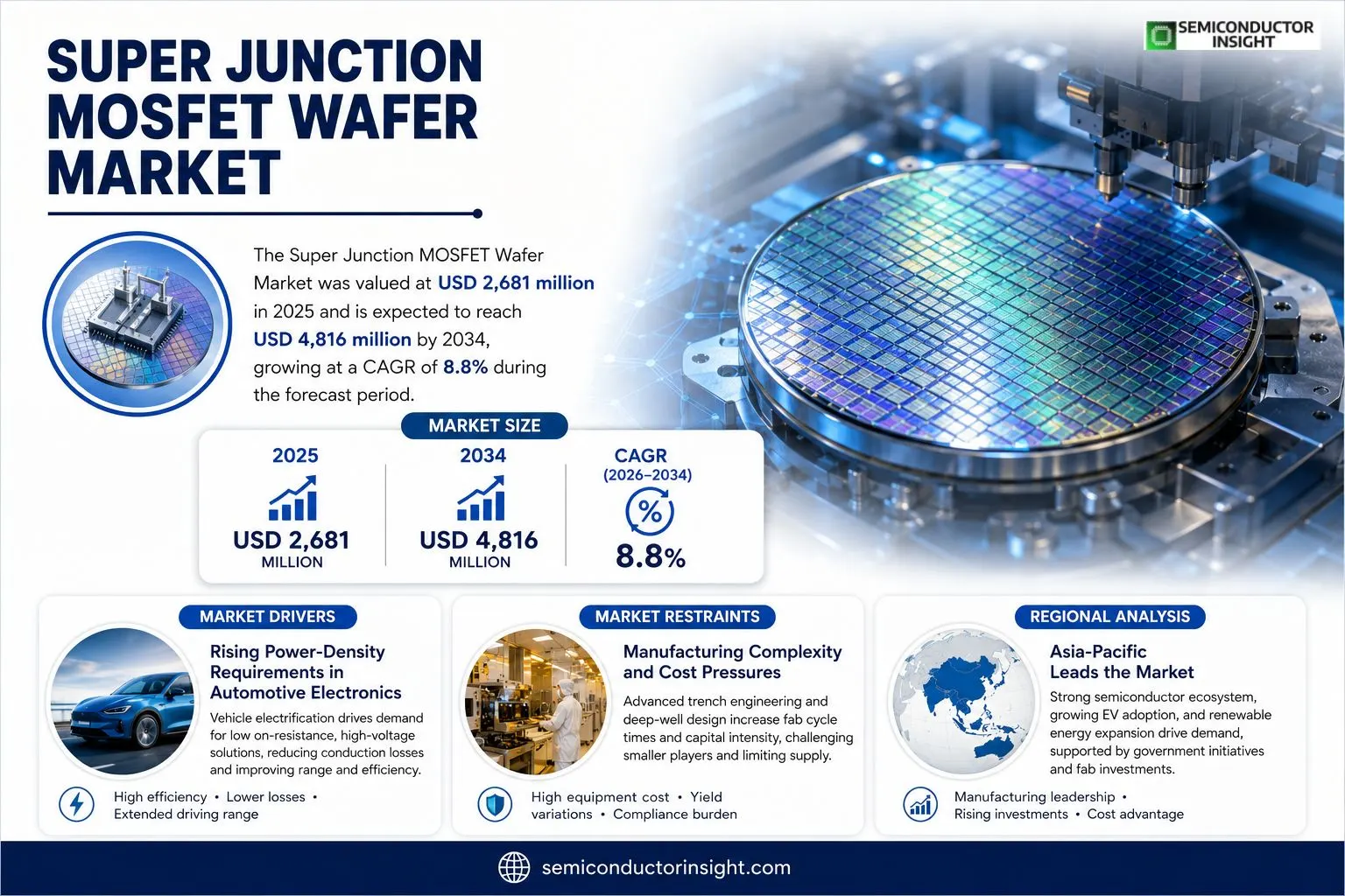
Super Junction MOSFET Wafer market was valued at USD 2,681 million in 2025. Sales reached roughly 3.9 million pieces that year at an average price of about USD 752 per wafer. Assuming the historic compound annual growth rate of 8.8 percent continues, the market is expected to expand to approximately USD 4,816 million by 2034.
Super Junction MOSFET Wafer refers to a processed silicon wafer on which super‑junction power MOSFET structures have been fabricated yet remain undiced. The architecture employs alternating P‑type and N‑type pillar regions within the drift zone, delivering high breakdown voltage while markedly lowering specific on‑resistance compared with conventional planar devices. Upstream inputs typically comprise prime silicon wafersoften epitaxially grownplus trench‑etching, refill or embedded epitaxy steps, CMP planarisation, ion implantation, gate formation and metallisation. Downstream activities involve wafer‑sort testing via probe cards, mapping, dicing and final assembly into discrete power modules or packaged devices.
MARKET DRIVERS
Rising Power‑Density Requirements in Automotive Electronics
Vehicle electrification pushes inverter modules toward higher power densities, compelling manufacturers to adopt **Super Junction MOSFET Wafer Market** solutions that can sustain lower on‑resistance while handling elevated voltages. The shift from conventional planar devices to super‑junction architectures reduces conduction losses, directly translating into extended driving range and lower thermal management costs.
Integration of Wide‑Bandgap Materials
Silicon‑carbide (SiC) and gallium‑nitride (GaN) platforms increasingly coexist with super‑junction wafers, creating hybrid power modules that capitalize on each technology’s strengths. Designers exploit the low‑capacitance profile of super‑junction MOSFETs to soften switching transients in SiC‑centric converters, a synergy that fuels demand for high‑yield wafer production.
➤ Analysts observe that the convergence of automotive efficiency targets and semiconductor material innovation accelerates fab investments across East Asia and the United States.
As OEMs set tighter efficiency benchmarks for next‑generation electric drivetrains, the volume of wafers processed in 2023 surpassed 1.1 million units, indicating that capacity expansions are already delivering economies of scale for downstream device manufacturers.
MARKET CHALLENGES
Manufacturing Complexity and Cost Pressures
The intricate trench formation and deep‑well engineering required for super‑junction structures elevate fab cycle times. While the performance payoff is clear, the incremental capital outlay for specialized equipment strains smaller players, limiting market entry and concentrating supply in a handful of high‑volume fabs.
Other Challenges
Yield Consistency
Achieving uniform dopant profiles across large‑diameter wafers remains a critical hurdle; slight variations can trigger premature breakdown, forcing manufacturers to implement extensive post‑process screening that inflates per‑unit costs.
MARKET RESTRAINTS
Regulatory and Environmental Constraints
Stringent emissions standards for semiconductor manufacturing, especially concerning hazardous chemicals used in trench etching, impose additional compliance burdens. Facilities that cannot demonstrate low‑impact processing may face production caps, curbing growth in regions with aggressive environmental policies.
MARKET OPPORTUNITIES
Emerging Renewable‑Energy Power‑Conversion Systems
Grid‑level inverters for solar and wind installations are transitioning to higher voltage tiers where super‑junction MOSFETs excel in minimizing conduction loss. This application segment projects a modest but steady uptick in wafer demand, encouraging fab operators to tailor process lines for smaller‑batch, high‑performance runs that serve niche renewable‑energy converters.
Super Junction MOSFET Wafer Market Trends
Efficiency‑Focused Adoption in Power Electronics
The demand for high‑efficiency conversion is reshaping the Super Junction MOSFET Wafer Market. In 2025, sales reached roughly 3.9 million pieces at an average price of US $752, delivering gross margins between 20 % and 30 %. Fast‑charging stations, server farms, and renewable‑energy converters all require lower conduction loss and tighter thermal budgets, prompting designers to replace conventional planar devices with super‑junction architectures. This migration is not simply a technology swap; it translates into smaller bill‑of‑materials, lighter system weight, and lower operating costs for end‑users. As manufacturers meet the tighter efficiency targets, wafer‑level yields become a decisive cost lever, with stable parametric performance directly influencing price competitiveness.
Other Trends
Supply‑Side Consolidation and Automation
Recent years have seen a pronounced shift toward larger‑diameter, high‑throughput fabs. Companies that have invested in 300 mm platforms and advanced epitaxial control are able to spread fixed‑costs over a broader output, achieving better unit economics and more resilient delivery schedules. Automation of deep‑trench etch, refill, and CMP steps reduces variability, thereby narrowing the spread in on‑resistance and breakdown voltage across the wafer. This operational tightening creates a cost advantage for suppliers with mature lines, while smaller players are compelled either to specialize in niche voltage classes or to form regional partnerships that mitigate capacity gaps.
Competitive Pressure from Wide‑Bandgap Alternatives
While silicon‑based super‑junction devices retain a strong foothold, the encroachment of SiC and GaN components in high‑power segments is forcing the Super Junction MOSFET Wafer Market to refine its value proposition. In voltage ranges where wide‑bandgap parts become cost‑prohibitive, super‑junction wafers are leveraged by optimizing system‑level gate‑drive schemes and integrating advanced packaging to squeeze out extra efficiency. This strategic alignment enables silicon solutions to occupy the “sweet spot” of performance versus cost, sustaining demand even as the broader power‑electronics ecosystem evolves toward ever‑higher power densities.
COMPETITIVE LANDSCAPE
Key Industry Players
Super Junction MOSFET Wafer Market: Competitive Overview
In the wafer segment, a handful of manufacturers command the bulk of capacity through vertically integrated epitaxy lines and automated trench‑fill processes. Infineon and STMicroelectronics each operate multi‑fab sites capable of 300‑mm production, leveraging tight charge‑balance control to deliver consistent on‑resistance and breakdown voltage. Toshiba’s silicon‑on‑insulator expertise translates into a robust portfolio that serves data‑center power modules, while Vishay’s diversified product mix adds depth in automotive‑grade voltage classes. Collectively, these firms occupy the top‑five share of sales in 2025, and their scale enables lower unit costs, stable supply lead times, and the ability to invest in next‑generation trench‑depth monitoring. Their competitive advantage is reinforced by a focus on high‑volume wafer‑sort testing and integrated design‑for‑manufacturing (DFM) practices that reduce yield variance across the 200‑mm and 300‑mm platforms.Beyond the dominant tier, a cohort of specialized players enriches the market with niche capabilities. Alpha and Omega Semiconductor (AOS) concentrates on high‑efficiency automotive‑grade wafers, employing custom epitaxial doping to meet stringent thermal constraints. PANJIT and IceMOS Technology have built reputations around rapid turnaround for telecom and renewable‑energy customers, often supplying 200‑mm items that fill gaps left by larger fabs. Hua Hong Semiconductor provides cost‑effective capacity for emerging Asian OEMs, while ON Semiconductor, ROHM, and Renesas leverage legacy power‑MOSFET lines to transition customers toward super‑junction architectures. Mitsubishi Electric, NXP Semiconductors, and Skyworks round out the landscape, each targeting specific voltage‑class segments or system‑level integration services that help manufacturers differentiate in crowded application spaces.
List of Key Super Junction MOSFET Wafer Companies Profiled
- Infineon Technologies AG
- STMicroelectronics
- Toshiba Electronic Devices & Storage Corporation
- Vishay Intertechnology
- Alpha and Omega Semiconductor (AOS)
- PANJIT
- IceMOS Technology
- Hua Hong Semiconductor
- ON Semiconductor
- ROHM Semiconductor
- Renesas Electronics Corporation
- Mitsubishi Electric Corporation
- NXP Semiconductors
Segment Analysis:
| Segment Category | Sub-Segments | Key Insights |
| By Type |
|
High‑Volume Wafer Sizes – The industry increasingly favors larger wafer footprints for cost efficiency; – 300mm platforms enable higher throughput while preserving tight dimensional control; – 200mm remains critical for legacy equipment and specialized processes; – Emerging formats respond to niche voltage and power density requirements. |
| By Application |
|
Efficiency‑Driven Power Conversion – Super‑junction wafers underpin applications demanding low loss; – Automotive electrification pushes demand for compact, high‑efficiency converters; – Data centers require reliable, high‑density power modules; – Telecom infrastructure benefits from fast‑response, thermally robust devices; – Renewable energy systems leverage the superior breakdown characteristics for higher voltage operation. |
| By End User |
|
Strategic End‑User Focus – End users prioritize reliability and thermal performance; – OEMs seek wafers that enable lighter, more compact power modules; – Data centers value consistency across large production batches; – Telecom makers look for devices that tolerate harsh RF environments and support rapid deployment cycles. |
| By Voltage Rating Class |
|
Voltage‑Optimized Offerings – Different voltage classes address distinct system needs; – 400 V devices are favored in low‑voltage automotive subsystems; – 600‑650 V platforms dominate industrial motor drives; – 800 V solutions enable higher power density for data‑center converters; – Flexibility across classes helps manufacturers match efficiency targets without over‑design. |
| By Qualification Grade |
|
Grade‑Specific Reliability – Qualification grades dictate robustness and testing depth; – Industrial grade emphasizes cost‑effective resilience for fixed‑location equipment; – Automotive grade adds stringent thermal cycling and vibration qualifications; – Military grade imposes the highest reliability standards, supporting mission‑critical platforms and extreme environments. |
Regional Analysis: Super Junction MOSFET Wafer Market
Asia-Pacific
Localized sourcing of high‑purity silicon and advanced diffusion equipment mitigates exposure to trans‑Pacific logistics disruptions, allowing foundries to sustain output even when freight constraints tighten.
Stricter emissions standards across China, India, and Southeast Asia press automotive manufacturers to adopt more efficient power stages, which directly lifts demand for the latest Super Junction wafers.
Universities in Singapore and Japan partner with leading fabs to prototype novel trench structures, accelerating the transition from pilot runs to volume production within a single technology node.
Competitive pressure has sparked a wave of process‑optimisation projects aimed at lowering per‑wafer expenditures without sacrificing breakdown voltage, a decisive factor for price‑sensitive market segments.
North America
In North America, the Super Junction MOSFET Wafer Market is shaped by a strong emphasis on reliability standards mandated by automotive safety programs and aerospace contracts. Tier‑1 suppliers are prioritising devices that demonstrate superior thermal performance under high‑current loads, prompting domestic fabs to refine their doping profiles. While the overall volume remains modest compared with the Asia‑Pacific region, the premium pricing associated with US‑based production yields healthy margins for players that can certify compliance with stringent quality certifications. Partnerships between equipment vendors and research labs foster incremental improvements in trench depth uniformity, a critical enabler for next‑generation electric‑bus powertrains.
Europe
European manufacturers are navigating a regulatory environment that elevates efficiency targets for industrial motor drives and renewable‑energy converters. Countries such as Germany and France incentivise the integration of high‑density power modules, which in turn raises the bar for wafer suppliers to deliver devices with minimal parasitic losses. The market is further differentiated by a cluster of specialist fabs that focus on niche applications, such as railway traction systems, where the balance between ruggedness and low on‑resistance is paramount. Collaborative initiatives across the EU aim to harmonise design libraries, enabling faster adoption of the latest Super Junction architectures in cross‑border projects.
South America
South American adoption of the Super Junction MOSFET Wafer Market is driven largely by expanding renewable‑energy farms and the gradual electrification of public transportation networks. Brazil’s growing solar‑panel manufacturing sector has sparked interest in power‑stage solutions that can handle fluctuating grid inputs, prompting local distributors to source wafers that combine high voltage tolerance with compact footprints. Although the regional production capacity is still emerging, strategic alliances with Asian manufacturers provide access to mature process technology, allowing South American firms to offer competitive solutions without establishing full‑scale fabs domestically.
Middle East & Africa
The Middle East & Africa region is witnessing a modest yet meaningful uptick in demand for high‑efficiency power devices, largely as a by‑product of large‑scale solar‑park deployments and the modernization of oil‑field control systems. Nations such as the United Arab Emirates and Saudi Arabia are investing in domestic semiconductor capabilities, emphasizing the need for wafers that can endure extreme temperature swings. Meanwhile, African markets are focusing on off‑grid electrification projects, where the reliability of Super Junction MOSFETs translates into longer service intervals for community power stations. This geographic spread creates pockets of opportunity for niche suppliers capable of tailoring their product mixes to the unique climatic and infrastructural constraints of the region.
Report Scope
This market research report provides a comprehensive analysis of the Super Junction MOSFET Wafer Market , covering the forecast period 2026–2034. It offers detailed insights into market dynamics, technological advancements, competitive landscape, and key trends shaping the industry.
Key focus areas of the report include:
- Market Overview: The report begins with an overview outlining its current market scenario, key growth indicators, and industry transformation drivers. It discusses macroeconomic factors, demand–supply balance, regulatory landscape, and the strategic role of semiconductors in powering advancements across industries such as automotive, telecommunications, consumer electronics, and industrial automation.
- Market Size & Forecast: Historical data and future projections for revenue, unit shipments, and market value across major regions and segments.
- Segmentation Analysis: Detailed breakdown by product type, technology, application, and end-user industry to identify high-growth segments and investment opportunities.
- Regional Insights: Insights into market performance across North America, Europe, Asia-Pacific, Latin America, and the Middle East & Africa, including country-level analysis where relevant.
- Competitive Landscape: Profiles of leading market participants, including their product offerings, R&D focus, manufacturing capacity, pricing strategies, and recent developments such as mergers, acquisitions, and partnerships.
- Technology Trends & Innovation: Assessment of emerging technologies, integration of AI/IoT, semiconductor design trends, fabrication techniques, and evolving industry standards.
- Market Drivers & Restraints: Evaluation of factors driving market growth along with challenges, supply chain constraints, regulatory issues, and market-entry barriers.
- Stakeholder Insights: Insights for component suppliers, OEMs, system integrators, investors, and policymakers regarding the evolving ecosystem and strategic opportunities.
Primary and secondary research methods are employed, including interviews with industry experts, data from verified sources, and real-time market intelligence to ensure the accuracy and reliability of the insights presented.
FREQUENTLY ASKED QUESTIONS:
What is the current market size of Super Junction MOSFET Wafer Market?
-> Super Junction MOSFET Wafer Market was valued at USD 2,681 million in 2025 and is expected to reach USD 4,816 million by 2034.
Which key companies operate in Super Junction MOSFET Wafer Market?
-> Key players include STMicroelectronics, Infineon, Toshiba, Vishay, Alpha and Omega Semiconductor (AOS), PANJIT, IceMOS Technology, and Hua Hong Semiconductor, among others.
What are the key growth drivers?
-> Key growth drivers include higher‑efficiency switch‑mode power conversion, demand for higher power density, expansion of fast‑charging infrastructure, growth of server and telecom power supplies, and increasing renewable/energy‑storage conversion needs.
Which region dominates the market?
-> Asia‑Pacific dominates the Super Junction MOSFET Wafer market, driven by extensive semiconductor manufacturing capacity and strong demand from automotive, data‑center, and telecom sectors.
What are the emerging trends?
-> Emerging trends include migration to larger wafer platforms (e.g., 300 mm), higher automation in fab lines, intensified competition with wide‑bandgap devices, advanced packaging and gate‑drive optimization, and system‑level reference designs to maximize wafer‑stage efficiency.
Get Sample Report PDF for Exclusive Insights
Report Sample Includes
- Table of Contents
- List of Tables & Figures
- Charts, Research Methodology, and more...
 Download Sample Report PDF